

INTEGRATED CIRCUITS
DATA SH EET
TDA4662
Baseband delay line
Product specification
Supersedes data of 1995 Oct 30
File under Integrated Circuits, IC02
1996 Nov 14
Philips Semiconductors Product specification
Baseband delay line TDA4662
FEATURES
• Two comb filters, using the switched-capacitor
technique, for one line delay time (64 µs)
• For PAL and NTSC
• Adjustment-free application
GENERAL DESCRIPTION
The TDA4662 is an integrated baseband delay line circuit
with one line delay. It is suitable for PAL and NTSC
decoders with colour-difference signal outputs±(R−Y) and
±(B−Y).
• Handles negative or positive colour-difference input
signals
• Clamping of AC-coupled input signals [±(R−Y) and
±(B−Y)]
• VCO without external components
• 3 MHz internal clock signal derived from a 6 MHz CCO,
line-locked by the sandcastle pulse (64 µs line)
• Sample-and-hold circuits and low-pass filters to
suppress the 3 MHz clock signal
• Addition of delayed and non-delayed output signals
• Output buffer amplifiers
• Comb filtering functions for NTSC colour-difference
signals to suppress cross-colour.
QUICK REFERENCE DATA
SYMBOL PARAMETER MIN. TYP. MAX. UNIT
V
P1
V
P2
I
P(tot)
V
i(p-p)
analog supply voltage (pin 9) 4.5 5 6 V
digital supply voltage (pin 1) 4.5 5 6 V
total supply current − 5.5 7.0 mA
±(R−Y) input signal PAL/NTSC (peak-to-peak value; pin 16) − 525 − mV
±(B−Y) input signal PAL/NTSC (peak-to-peak value; pin 14) − 665 − mV
G
v
voltage gain VO/VI of colour-difference output signals
V
V
for PAL and NTSC 5.3 5.8 6.3 dB
11/V16
for PAL and NTSC 5.3 5.8 6.3 dB
12/V14
ORDERING INFORMATION
TYPE
NUMBER
NAME DESCRIPTION VERSION
PACKAGE
TDA4662 DIP16 plastic dual in-line package; 16 leads (300 mil) SOT38-4
TDA4662T SO16 plastic small outline package; 16 leads; body width 3.9 mm SOT109-1
1996 Nov 14 2
Philips Semiconductors Product specification
Baseband delay line TDA4662
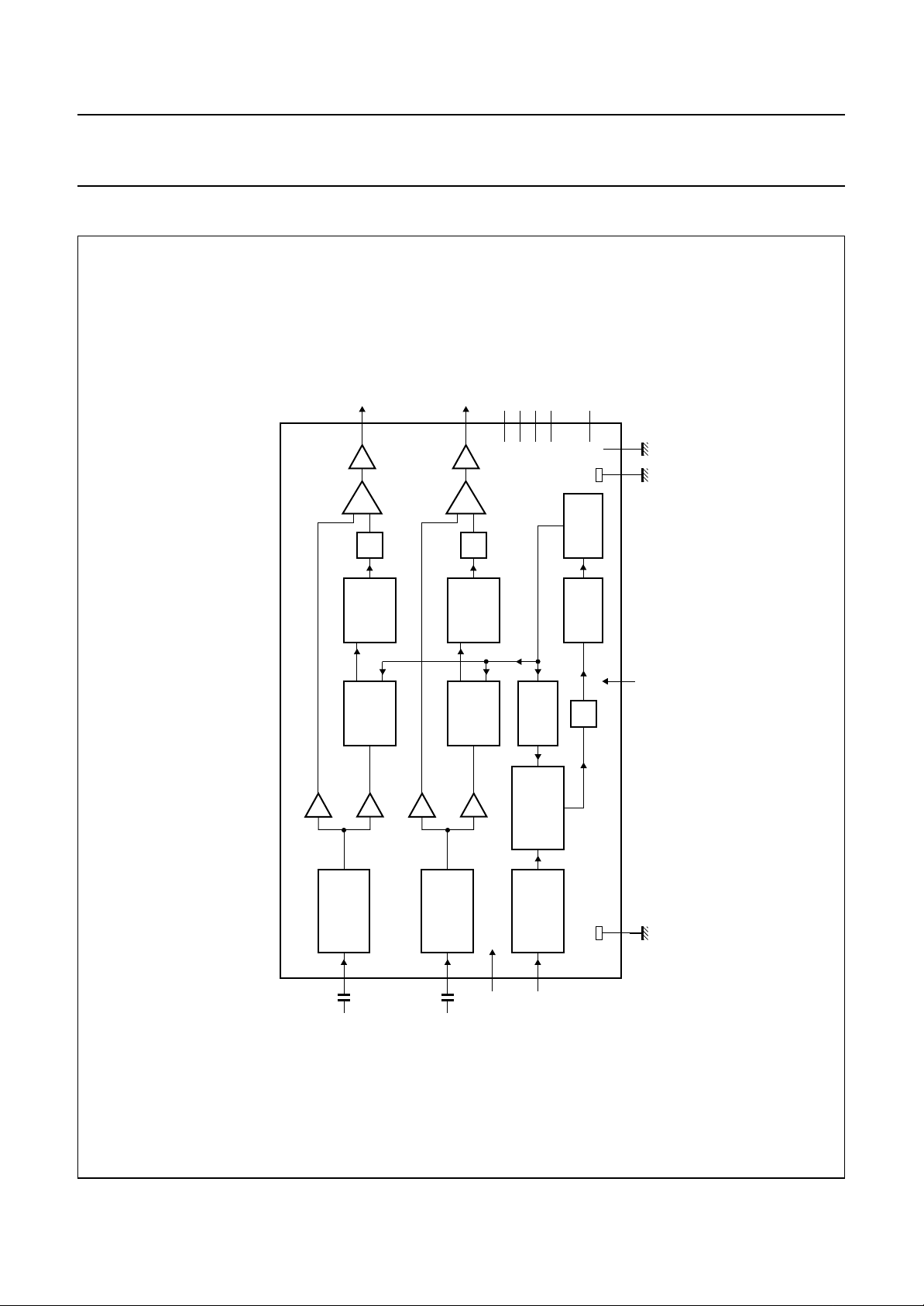
BLOCK DIAGRAM
±(R−Y)
11
LP
SAMPLE-
AND-HOLD
LINE
MEMORY
output signals
colour-difference
12
output
buffers
stages
addition
pre-amplifiers
±(B−Y)
2
LP
SAMPLE-
AND-HOLD
LINE
MEMORY
n.c.
n.c.13n.c.15n.c.7i.c.
6
TDA4662
3 MHz shifting clock
BY-192
DIVIDE-
PHASE
DETECTOR
FREQUENCY
BY-2
DIVIDE-
CCO
6 MHz
LP
MED743
4, 8
3
GND2
1
P2
V
digital supply
Fig.1 Block diagram.
SIGNAL
CLAMPING
16
±(R−Y)
handbook, full pagewidth
colour-difference
SIGNAL
14
±(B−Y)
input signals
1996 Nov 14 3
CLAMPING
analog supply
9
P1
V
DETECTOR
SANDCASTLE
5
input
sandcastle
10
GND1
Philips Semiconductors Product specification
Baseband delay line TDA4662
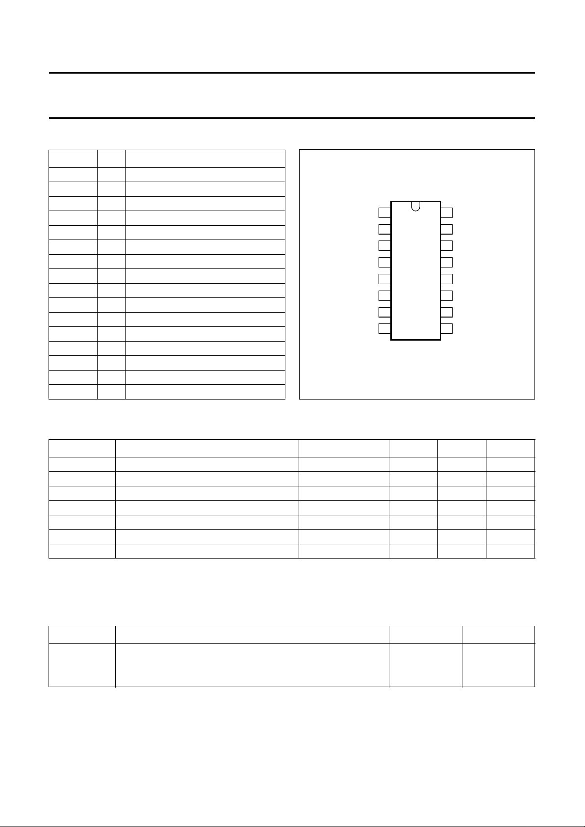
PINNING
SYMBOL PIN DESCRIPTION
V
P2
n.c. 2 not connected
GND2 3 ground for digital part (0 V)
i.c. 4 internally connected
SAND 5 sandcastle pulse input
n.c. 6 not connected
i.c. 7 internally connected
i.c. 8 internally connected
V
P1
GND1 10 ground for analog part (0 V)
V
o(R−Y)
V
o(B−Y)
n.c. 13 not connected
V
i(B−Y)
n.c. 15 not connected
V
i(R−Y)
1 supply voltage for digital part (+5 V)
9 supply voltage for analog part (+5 V)
11 ±(R−Y) output signal
12 ±(B−Y) output signal
14 ±(B−Y) input signal
16 ±(R−Y) input signal
handbook, halfpage
V
1
P2
n.c.
2
3
GND2
4
i.c.
SAND
n.c.
i.c.
i.c.
5
6
7
8
TDA4662
MED744
Fig.2 Pin configuration.
16
V
i(R−Y)
15
n.c.
14
V
i(B−Y)
13
n.c.
12
V
o(B−Y)
11
V
o(R−Y)
10
GND1
9
V
P1
LIMITING VALUES
In accordance with the Absolute Maximum Rating System (IEC 134). Ground pins 3 and 10 connected together.
SYMBOL PARAMETER CONDITIONS MIN. MAX. UNIT
V
V
V
V
T
T
V
P1
P2
5
n
stg
amb
ESD
supply voltage (pin 9) −0.5 +7 V
supply voltage (pin 1) −0.5 +7 V
input voltage on pin 5 −0.5 VP+ 1.0 V
voltage on pins 11, 12, 14 and 16 −0.5 V
P
V
storage temperature −25 +150 °C
operating ambient temperature 0 70 °C
electrostatic handling for all pins note 1 −±500 V
Note
1. Equivalent to discharging a 200 pF capacitor through a 0 Ω series resistor.
THERMAL CHARACTERISTICS
SYMBOL PARAMETER VALUE UNIT
R
th j-a
thermal resistance from junction to ambient in free air
SOT38-4 75 K/W
SOT109-1 220 K/W
1996 Nov 14 4
 Loading...