

Philips tda4662 DATASHEETS
INTEGRATED CIRCUITS
DATA SH EET
TDA4662
Baseband delay line
Product specification
Supersedes data of 1995 Oct 30
File under Integrated Circuits, IC02
1996 Nov 14
Philips Semiconductors Product specification
Baseband delay line TDA4662
FEATURES
• Two comb filters, using the switched-capacitor
technique, for one line delay time (64 µs)
• For PAL and NTSC
• Adjustment-free application
GENERAL DESCRIPTION
The TDA4662 is an integrated baseband delay line circuit
with one line delay. It is suitable for PAL and NTSC
decoders with colour-difference signal outputs±(R−Y) and
±(B−Y).
• Handles negative or positive colour-difference input
signals
• Clamping of AC-coupled input signals [±(R−Y) and
±(B−Y)]
• VCO without external components
• 3 MHz internal clock signal derived from a 6 MHz CCO,
line-locked by the sandcastle pulse (64 µs line)
• Sample-and-hold circuits and low-pass filters to
suppress the 3 MHz clock signal
• Addition of delayed and non-delayed output signals
• Output buffer amplifiers
• Comb filtering functions for NTSC colour-difference
signals to suppress cross-colour.
QUICK REFERENCE DATA
SYMBOL PARAMETER MIN. TYP. MAX. UNIT
V
P1
V
P2
I
P(tot)
V
i(p-p)
analog supply voltage (pin 9) 4.5 5 6 V
digital supply voltage (pin 1) 4.5 5 6 V
total supply current − 5.5 7.0 mA
±(R−Y) input signal PAL/NTSC (peak-to-peak value; pin 16) − 525 − mV
±(B−Y) input signal PAL/NTSC (peak-to-peak value; pin 14) − 665 − mV
G
v
voltage gain VO/VI of colour-difference output signals
V
V
for PAL and NTSC 5.3 5.8 6.3 dB
11/V16
for PAL and NTSC 5.3 5.8 6.3 dB
12/V14
ORDERING INFORMATION
TYPE
NUMBER
NAME DESCRIPTION VERSION
TDA4662 DIP16 plastic dual in-line package; 16 leads (300 mil) SOT38-4
TDA4662T SO16 plastic small outline package; 16 leads; body width 3.9 mm SOT109-1
1996 Nov 14 2
PACKAGE
Philips Semiconductors Product specification
Baseband delay line TDA4662
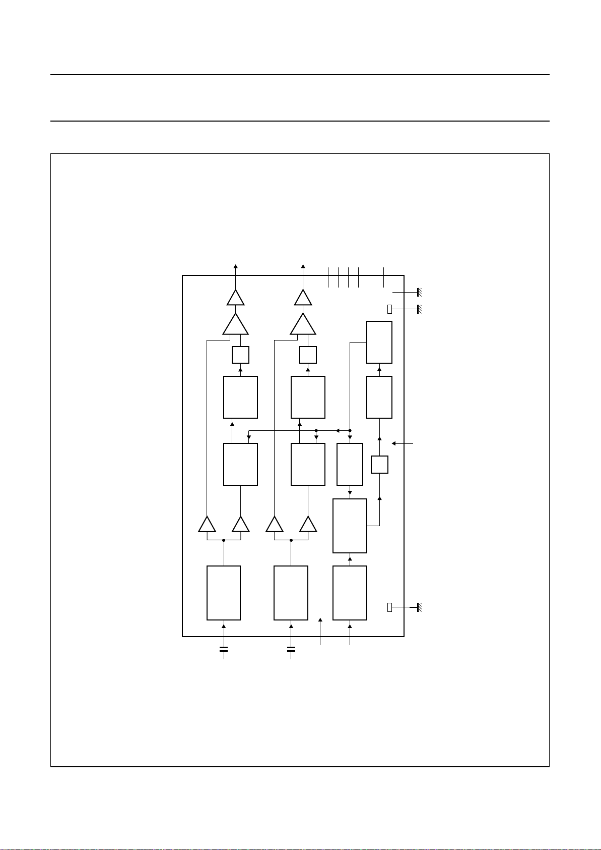
BLOCK DIAGRAM
±(R−Y)
11
LP
SAMPLE-
AND-HOLD
LINE
MEMORY
output signals
colour-difference
12
output
buffers
stages
addition
pre-amplifiers
±(B−Y)
2
LP
SAMPLE-
AND-HOLD
LINE
MEMORY
n.c.
n.c.13n.c.15n.c.7i.c.
6
TDA4662
3 MHz shifting clock
BY-192
DIVIDE-
PHASE
DETECTOR
FREQUENCY
BY-2
DIVIDE-
CCO
6 MHz
LP
MED743
4, 8
3
GND2
1
P2
V
digital supply
Fig.1 Block diagram.
1996 Nov 14 3
SIGNAL
CLAMPING
16
±(R−Y)
handbook, full pagewidth
SIGNAL
CLAMPING
14
±(B−Y)
input signals
colour-difference
analog supply
5
9
P1
V
DETECTOR
SANDCASTLE
input
sandcastle
10
GND1
 Loading...