

Philips TDA4655 Datasheet

INTEGRATED CIRCUITS
DATA SH EET
TDA4655
Generic multi-standard decoder
Preliminary specification
File under Integrated Circuits, IC02
June 1993
Philips Semiconductors Preliminary specification
Generic multi-standard decoder TDA4655
FEATURES
• Low voltage (8 V)
• Low power dissipation (250 mW)
• Automatic standard recognition
• No adjustments required
GENERAL DESCRIPTION
The TDA4655 is a monolithic integrated multi-standard
colour decoder for PAL, SECAM and NTSC (3.58 and
4.43 MHz) with negative colour difference output signals.
It is adapted to the integrated baseband delay line
TDA4660/61.
• Reduced external components
• Not all time constants integrated (ACC, SECAM
de-emphasis).
QUICK REFERENCE DATA
SYMBOL PARAMETER CONDITIONS MIN. TYP. MAX. UNIT
Supply
V
P
I
P
P
tot
supply voltage 7.2 8.0 8.8 V
supply current VP= 8.0 V; without load 25 31 37 mA
total power dissipation VP= 8.0 V; without load − 248 296 mW
Inputs
V
11
V
24
chrominance input voltage (peak-to-peak value) note 1 20 200 400 mV
sandcastle input voltage −− 13.2 V
Outputs
V1 colour difference output signals
independent of supply voltage; note 2
(peak-to-peak value)
−(R−Y) output PAL and NTSC 4.43 MHz 442 525 624 mV
NTSC 3.58 MHz 370 440 523 mV
SECAM 950 1050 1150 mV
V
3
−(B-Y) output PAL and NTSC 4.43 MHz 559 665 791 mV
NTSC 3.58 MHz 468 557 662 mV
SECAM 1200 1330 1460 mV
Notes to quick reference data
1. Within 2 dB output voltage deviation.
2. Burstkey width for PAL 4.3 µs, for NTSC 3.6 µs.
Burst width for PAL and NTSC 2.25 µs ratio burst chrominance amplitude 1/2.2.
ORDERING INFORMATION
EXTENDED
TYPE NUMBER
PINS PIN POSITION MATERIAL CODE
PACKAGE
TDA4655 24 SDIL plastic SOT234
TDA4655T 24 SO plastic SOT137A
Note
1. SOT234-1; 1996 November 26.
2. SOT137-1; 1996 November 26.
June 1993 2
(1)
(2)
Philips Semiconductors Preliminary specification
Generic multi-standard decoder TDA4655
June 1993 3
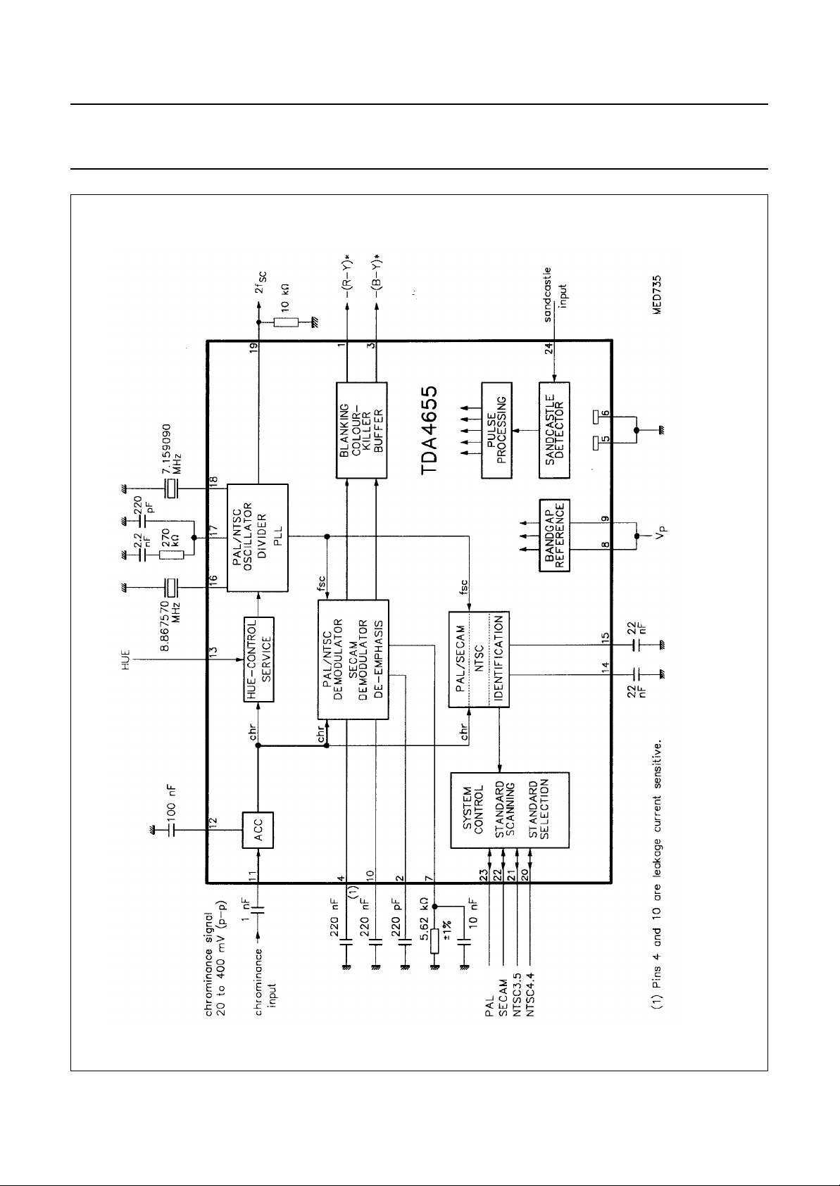
Fig.1 Block diagram.
Philips Semiconductors Preliminary specification
Generic multi-standard decoder TDA4655
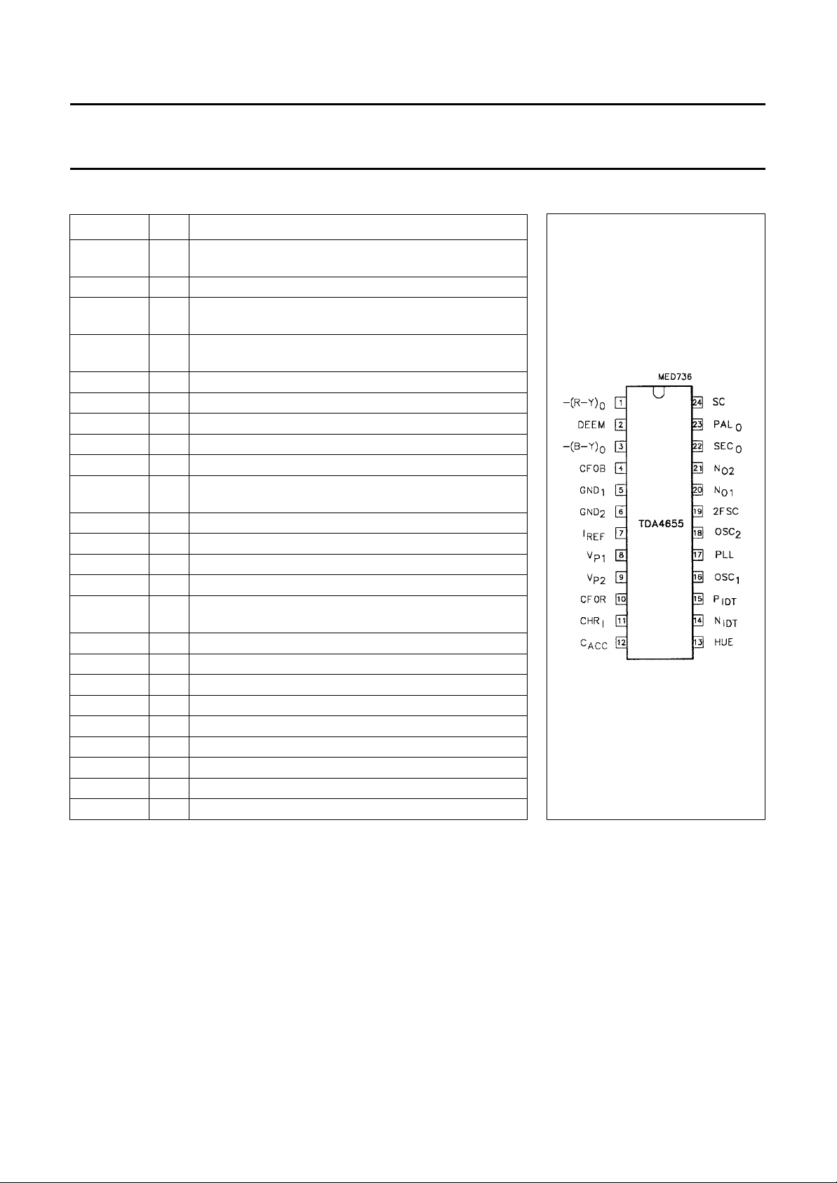
PINNING
SYMBOL PIN DESCRIPTION
−(R−Y)o 1 colour difference signal output −(R−Y)* for baseband
delay line
DEEM 2 external capacitor for SECAM de-emphasis
−(B−Y)o 3 colour difference signal output −(B−Y)* for baseband
delay line
CFOB 4 external capacitor SECAM demodulator control (B−Y)
Channel
GND
1
GND
2
I
REF
V
P1
V
P2
CFOR 10 external capacitor SECAM demodulator control (R−Y)
CHR
I
C
ACC
HUE 13 input for HUE control and service switch
N
IDT
P
IDT
OSC
1
PLL 17 external loop filter
OSC
2
2FSC 19 2 × f
N
O1
N
O2
SEC
O
PAL
O
SC 24 sandcastle input
5 ground
6 ground
7 external resistor for SECAM oscillator
8 supply 8 V
9 supply 8 V
Channel
11 chrominance signal input
12 external capacitor for ACC control
14 external capacitor for identification circuit (NTSC)
15 external capacitor for identification circuit (PAL and
SECAM)
16 PAL crystal
18 NTSC crystal
output
SC
20 standard setting input/output for NTSC 4.43
21 standard setting input/output for NTSC 3.58
22 standard setting input/output for SECAM
23 standard setting input/output for PAL
Fig.2 Pin configuration.
June 1993 4

Philips Semiconductors Preliminary specification
Generic multi-standard decoder TDA4655
FUNCTIONAL DESCRIPTION
The IC contains all functions required
for the identification and
demodulation of signals with the
standards PAL, SECAM, NTSC 3.5
with 3.58 MHz colour-carrier
frequency and NTSC 4.3 with
4.43 MHz colour-carrier frequency.
When an unknown signal is fed into
the input, the circuit has to detect the
standard of the signal, and has to
switch on successively the
appropriate input filter, crystal (8.8 or
7.2 MHz) and demodulator and
finally, after having identified the
signal, it has to switch on the colour
and, in event of NTSC reception, the
hue control. At the outputs the two
colour difference signals−(R−Y)* and
-(B−Y)* are available. The
identification circuit is able to
discriminate between NTSC signals
with colour-carrier frequencies of
3.58 MHz or 4.43 MHz.
ACC-stage
The chrominance signal is fed into the
asymmetrical input (pin 11) of the
ACC-stage (Automatic Colour
Control). The input has to be AC
coupled and has an input impedance
of 20 kΩ in parallel with 10 pF.
To control the chrominance amplitude
the modulation independent burst
amplitude is measured during the
burstkey pulse which is derived from
the sandcastle pulse present at pin
24. The generated error current is fed
into an external storage capacitor at
pin 12. The integrated error voltage
controls the gain of the ACC stage so
that its output is independent of input
signal variations.
The measurement is disabled during
the vertical blanking to avoid failures
because of missing burst signals.
Reference signal generation
The reference signal generation is
achieved by a PLL system. The
reference oscillator operates at twice
the colour-carrier frequency and is
locked on the burst of the
chrominance signal (chr). A divider
provides reference signals (fSC) with
the correct phase relationship for the
PAL/NTSC demodulator and the
identification part. In the SECAM
mode the two f0 frequencies are
derived from the PAL crystal
frequency by special dividers. In this
mode the oscillator is not locked to
the input signal. In the NTSC mode
the hue control circuit is switched
between ACC stage and PLL. The
phase shift of the signal can be
controlled by a DC voltage at pin 13.
The hue control circuit is switched off
during scanning. The reference
frequency (2 × fSC) is available at pin
19 to drive a PAL comb filter for
example.
Demodulation
The demodulation of the colour signal
requires two demodulators. One is
common for PAL and NTSC signals,
the other is for SECAM signals.
The PAL/NTSC demodulator consists
of two synchronized demodulators,
one for the (B−Y) Channel and the
other for the (R−Y) Channel. The
required reference signals (f
input from the reference oscillator. In
NTSC mode the PAL switch is
disabled.
The SECAM demodulator consists of
a PLL system. During vertical
blanking the PLL oscillator is tuned to
the f0 frequencies to provide a fixed
black level at the demodulator output.
During demodulation the control
voltages are stored in the external
capacitors at pins 4 and 10.
The oscillator requires an external
resistor at pin 7. Behind the PLL
demodulator the signal is fed into the
de-emphasis network which consists
SC
) are
of two internal resistors (2.8 kΩ and
5.6 kΩ) and an external capacitor
connected at pin 2 (220 pF).
After demodulation the signal is
filtered and then fed into the next
stage.
Blanking, colour-killer, buffers
As a result of using only one
demodulator in SECAM mode the
demodulated signal has to be split up
in the (B−Y) Channel and the (R−Y)
Channel. The unwanted signals
occuring every second line, (R−Y) in
the (B−Y) Channel and (B−Y) and in
the (R−Y) Channel, have to be
blanked. This happens in the blanking
stage by an artificial black level being
inserted alternately every second
line.
To avoid disturbances during line and
field flyback these parts of the colour
differential signals are blanked in all
modes.
When no signal has been identified,
the colour is switched off (signals are
blanked) by the colour killer. At the
end of the colour channels are
low-ohmic buffers (emitter followers).
The CD output signals −(B−Y)* and
−(R−Y)* are available at pins 1 and 3.
Identification and system control
The identification part contains three
identification demodulators.
The first demodulates in PAL mode. It
is only active during the burstkey
pulse. The reference signal (f
the (R−Y) phase.
The second demodulator (PLL
system) operates in SECAM mode
and is active also during the burstkey
pulse, but delayed by 2 µs.
The PLL demodulator discriminates
the frequency difference between the
unmodulated f0 frequencies of the
incoming signal (chr) and the
reference frequency input from the
crystal oscillator.
These two demodulators are followed
by an H/2 switch ‘rectifying’ the
SC
) has
June 1993 5
Philips Semiconductors Preliminary specification
Generic multi-standard decoder TDA4655
demodulated signal. The result is an
identification signal (P
pin 15) that
IDT,
is positive for a PAL signal in PAL
mode, for a SECAM signal in SECAM
mode and for a PAL signal in
NTSC 4.4 mode.
If P
is positive in SECAM mode,
IDT
the scanner switches back to the PAL
mode in order to prevent a PAL signal
being erroneously identified as a
SECAM signal (PAL priority). If then
P
is not positive, the scanner
IDT
returns to SECAM mode and remains
there until P
is positive again. In
IDT
the event of a field frequency of 60 Hz
the signal can not be identified as a
SECAM signal, even if P
IDT
is
positive. In this event the scanner
switches forward in the NTSC 3.5
mode. If the H/2 signal has the wrong
polarity, the identification signal is
negative and the H/2 flip-flop is set to
the correct phase.
The third demodulator operates in
NTSC mode and is active during the
burstkey pulse. The resulting
identification signal (N
, pin 14) is
IDT
positive for PAL and NTSC 4.4
signals in NTSC 4.4 mode and for
NTSC 3.5 signals in the NTSC 3.5
mode. The reference signal has the
(B−Y) phase.
The two identification signals allow an
unequivocal identification of the
received signal. In the event of a
signal being identified, the scanning is
stopped and after a delay time the
colour is switched on.
The standard outputs (active HIGH)
are available at the pins 20, 21, 22
and 23. During scanning the HIGH
level is 2.5 V and when a signal has
been identified the HIGH level is
switched to 6 V. The standard pins
can also be used as inputs in order to
force the IC into a desired mode
(Forced Standard Setting).
Sandcastle detector and pulse processing
In the sandcastle detector the super
sandcastle pulse (SC) present at pin
24 is compared with three internal
threshold levels by means of three
differential amplifiers. The derived
signals are the burstkey pulse, the
horizontal blanking pulse and the
combined horizontal and vertical
blanking pulse. These signals are
processed into various control pulses
required for the timing of the IC.
Bandgap reference
In order to ensure that the CD output
signals and the threshold levels of the
sandcastle detector are independent
of supply voltage variations a
bandgap reference voltage has been
integrated.
LIMITING VALUES
In accordance with the Absolute Maximum Rating System (IEC 134).
SYMBOL PARAMETER CONDITIONS MIN. MAX. UNIT
T
T
V
P
V
stg
amb
p
tot
24
storage temperature −25 +150 °C
operating ambient temperature 0 +70 °C
supply voltage − 8.8 V
power dissipation without load − 330 mW
voltage at pin 24 I
voltage at all other pins I
=10µA − 15 V
max
= 100 µA − VP+
max
V
be
THERMAL RESISTANCE
SYMBOL PARAMETER THERMAL RESISTANCE
R
th j-a
thermal resistance on printed-circuit board from
junction to ambient in free air (without heat spreader)
SO 24 90 K/W
SDIL 24 70 K/W
V
June 1993 6
 Loading...