

Philips TDA4651WP, TDA4651 Datasheet

INTEGRATED CIRCUITS
DATA SH EET
TDA4651
Multistandard colour decoder with
negative colour difference output
signals
Preliminary specification
File under Integrated Circuits, IC02
August 1993

Philips Semiconductors Preliminary specification
Multistandard colour decoder with negative
colour difference output signals
FEATURES
Identifies and demodulates PAL,
SECAM, NTSC 3.58 and NTSC 4.43
chrominance signals with:
• Gain controlled chrominance
amplifier
• ACC demodulation controlled by
system scanning
• Internal colour difference signal
output filters to remove the residual
subcarrier
• PAL / NTSC demodulation
– H (burst) and V blanking
– PAL switch (disabled for NTSC)
– NTSC phase shift (disabled for
PAL)
– PLL-controlled reference
oscillator
– two reference oscillator crystals
on separate pins with automatic
switching
– quadrature demodulator with
subcarrier reference
• SECAM demodulation
– limiter amplifier
– quadrature demodulator with a
single external reference tuned
circuit
– alternate line blanking, H and V
blanking
– de-emphasis
• Identification
– automatic standard identification
by sequential inquiry
– secure SECAM identification at
50 Hz only, with PAL priority
– four switched outputs for
chrominance filter selection and
display control
– external service switch for
oscillator adjustment
GENERAL DESCRIPTION
The TDA4651 is a monolithic integrated multistandard colour decoder for PAL,
SECAM and NTSC (3.58 and 4.43 MHz) with negative colour difference output
signals. The colour difference output signals are fed to the TDA4661, switched
capacitor delay line.
QUICK REFERENCE DATA
SYMBOL PARAMETER CONDITIONS MIN. TYP. MAX. UNIT
V
P
positive
supply voltage
(pin 13)
I
P
supply current
(pin 13)
V
i(p-p)
chrominance
input voltage
(pin 15)
(peak-to-peak
value)
Colour difference output signals (see note 2)
V
1(p-p)
−(R−Y) output
(peak-to-peak
value)
V
3(p-p)
−(B−Y) output
(peak-to-peak
value)
Notes to quick reference data
1. Within 3 dB output voltage deviation.
2. Burst key width for PAL 4.3 µs, for NTSC 3.6 µs
Burst width for PAL and NTSC 2.25 µs, ratio burst-chrominance-amplitude
1/2.2.
ORDERING INFORMATION
EXTENDED
TYPE NUMBER
PINS
TDA4651 28 DIL plastic SOT117
TDA4651WP 28 PLCC plastic SOT261CG
Note
1. SOT117-1; 1996 November 25.
2. SOT261-2; 1996 November 25.
TDA4651
10.8 12 13.2 V
− 60 − mA
see note 1 20 200 400 mV
PAL 442 525 624 mV
NTSC 370 440 523 mV
SECAM 883 1050 1248 mV
PAL 559 665 791 mV
NTSC 468 557 662 mV
SECAM 1119 1330 1581 mV
PACKAGE
PIN
POSITION
MATERIAL CODE
(1)
(2)
August 1993 2
Philips Semiconductors Preliminary specification
Multistandard colour decoder with negative
colour difference output signals
TDA4651
August 1993 3
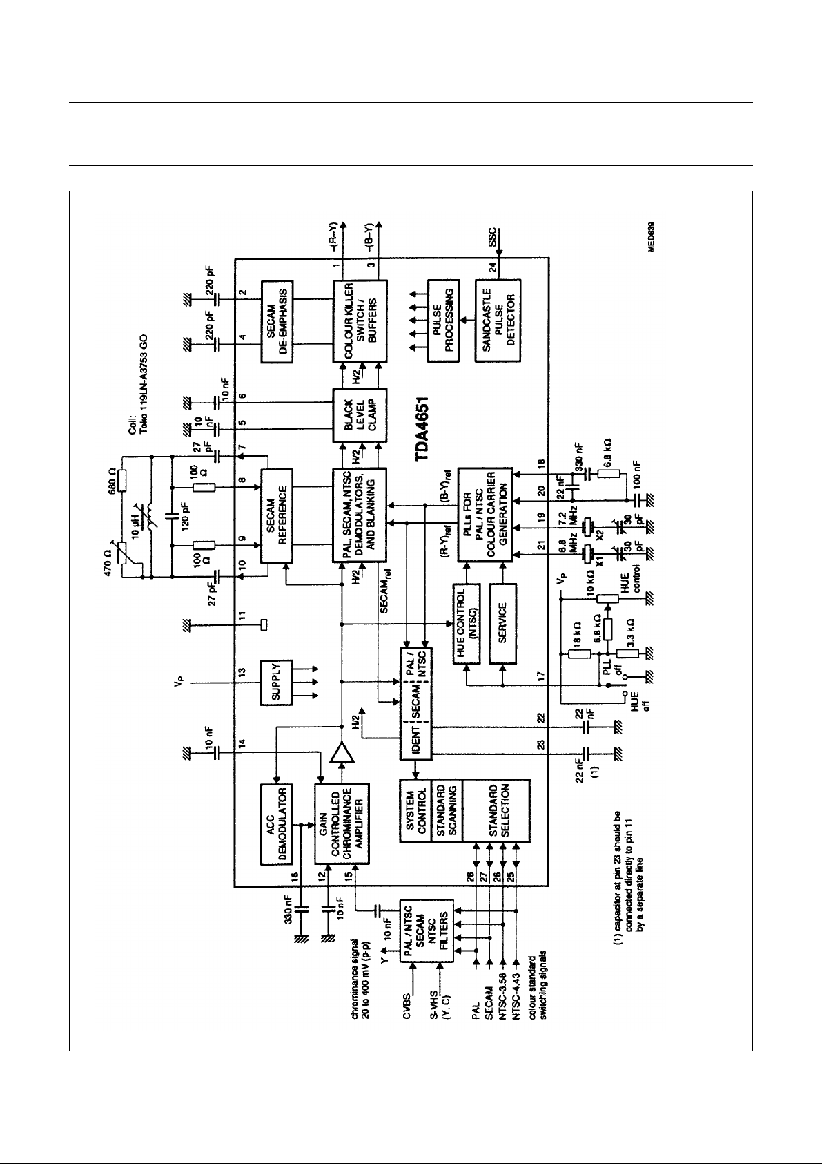
Fig.1 Block diagram.
Philips Semiconductors Preliminary specification
Multistandard colour decoder with negative
colour difference output signals
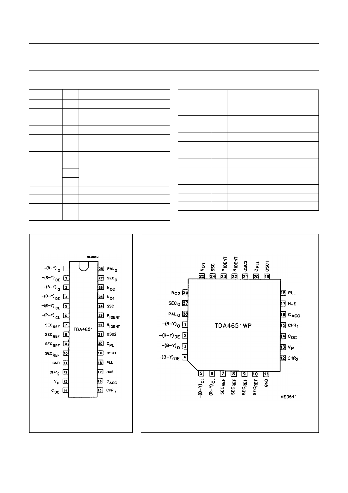
PINNING
SYMBOL PIN DESCRIPTION
−(R−Y)
o
−(R−Y)
DE
−(B−Y)
o
−(B−Y)
DE
−(B−Y)
CL
−(R−Y)
CL
SEC
REF
GND 11 ground
CHR
2
V
P
C
DC
1 −(R−Y) output
2(R−Y) de-emphasis
3 −(B−Y) output
4(B−Y) de-emphasis
5(B−Y) clamping
6(R−Y) clamping
7 SECAM reference tuned circuit
8
9
10
12 DC for ACC
13 supply voltage
14 DC feedback
TDA4651
CHR
1
C
ACC
HUE 17 hue control
PLL 18 PLL time constant
OSC1 19 input for 7.15 MHz oscillator
C
PLL
OSC2 21 input for 8.86 MHz oscillator
N
IDENT
P
IDENT
SSC 24 super sandcastle pulse input
N
01
N
02
SEC
0
PAL
0
15 chrominance input
16 automatic colour control
20 PLL DC reference
22 NTSC identification
23 PAL/SECAM identification
25 NTSC (4.43 MHz) identification
26 NTSC (3.58 MHz) identification
27 SECAM identification
28 PAL identification
Fig.2 Pin configuration for DIL
package.
August 1993 4
Fig.3 Pin configuration for PLCC package.

Philips Semiconductors Preliminary specification
Multistandard colour decoder with negative
colour difference output signals
FUNCTIONAL DESCRIPTION
The IC (see block diagram Fig.1)
contains all functions required for the
identification and demodulation of
PAL, SECAM, NTSC 4.43 MHz and
NTSC 3.58 MHz signals. When an
unknown signal is fed into the input,
the circuit has to identify the standard
of the signal; to achieve this it has to
switch on successively the
appropriate input filter, crystal (8.8 or
7.2 MHz) and demodulator and
finally, after having identified the
signal, it has to switch on the colour
and, in the event of NTSC reception,
the hue control. The two colour
difference signals −(R−Y) and−(B−Y)
are available at the outputs. The
identification circuit is able to
discriminate between NTSC signals
with colour carrier frequencies of
3.58 MHz or 4.43 MHz.
Chrominance amplifier
The chrominance amplifier has an
asymmetrical input. The input signal
has to be AC coupled (pin 15). The
differential amplifier stage at the input
is followed by the gain control stage
and a differential amplifier with lateral
PNP transistors having the function of
a level shifter. The gain control stage
consists of two ACC-rectifier circuits.
One rectifier circuit is switched on
during SECAM reception respectively
during the SECAM part of the
system-control-scanning (it is
switched on during part of the burst
gate pulse and it is disabled during
the prolonged frame flyback); the
other rectifier is switched on during
the burst, when PAL or NTSC signals
are received respectively during the
PAL and NTSC parts of the system
control scanning. The DC-potential of
the symmetrical signal connections to
the demodulators is kept at the same
level by means of a working point
control stage.
Reference oscillator
The reference oscillator for PAL and
NTSC operates at twice the colour
carrier frequency. It is followed by a
divider stage, providing the (R−Y) and
(B−Y) reference signal with the
correct phase relation to the
PAL/NTSC demodulator and the
identification part.
Demodulators
The demodulation of the colour signal
requires three demodulators. Two are
common for PAL and NTSC and one
for the SECAM signals. In the event of
NTSC reception, the symmetrical
signal is fed into two differential
amplifier stages with the correct gain
and from there the signal is fed into
two demodulators each consisting of
four transistors. During NTSC
reception the PAL switch between the
differential amplifier of the (R-Y)
channel and the corresponding
demodulator is disabled. These
transistors are switched on and off by
the appropriate reference signals. In
the event of PAL reception, the
symmetrical signal is fed into the
same differential amplifiers and the
PAL switch is active.
The SECAM demodulator is a
combined demodulator for −(B−Y)
and −(R−Y) with artificial black level
being inserted alternately every
second line and during line and field
flyback. The load resistors of the
demodulator are connected to two
differential amplifiers, one for −(B−Y)
and one for −(R−Y). The unwanted
signals occurring every second line
((R−Y) in the −(B−Y) channel and
(B−Y) in the −(R−Y) channel) are
blanked.
TDA4651
Clamp
Behind the demodulators the signals
are being filtered and the black level
is clamped to a constant DC-level
during the burst gate pulse. For the
SECAM signals this happens every
second line, when the appropriate
artificial black level is present.
De-emphasis and output-buffer
Behind the clamping stages is the
de-emphasis for the SECAM signals
and just in front of the output stages
are the colour killer and blanking
stages. The blanking level is the
same as the clamping level and the
black level.
Identification
The identification part contains three
demodulators.
The first is demodulating during PAL
and NTSC identification or reception.
It is active during the burst clamping
only. The reference signal has the
(R-Y)-phase. The second
demodulator is demodulating during
the SECAM identification or reception
and is active during part of the burst
clamping time. It uses the same
signals as the SECAM demodulator
that is not active during field flyback.
These two demodulators are followed
by a H/2 switch ‘rectifying’ the
demodulated signal. The result is an
identification signal (P
positive for a PAL signal during the
PAL part of the scanning, for a
SECAM signal during the SECAM
part of the scanning and for a PAL
signal during the NTSC 4.43 part of
the scanning. If the P
during the SECAM part of the
scanning, the scanner switches back
to the PAL part of the scanning in
order to prevent that a PAL signal is
erroneously identified as a SECAM
signal (PAL priority).
If then the P
scanner returns to SECAM part and
remains there until the P
is not positive, the
IDENT
IDENT
IDENT
) that is
is positive
IDENT
is
August 1993 5
 Loading...