

Philips TDA4650WP-V4, TDA4650-V4 Datasheet

DATA SH EET
Preliminary specification
File under Integrated Circuits, IC02
March 1991
INTEGRATED CIRCUITS
TDA4650
Multistandard colour decoder, with
negative colour difference output
signals
March 1991 2
Philips Semiconductors Preliminary specification
Multistandard colour decoder, with negative
colour difference output signals
TDA4650
FEATURES
Identifies and demodulates PAL,
SECAM, NTSC 3.58 and NTSC 4.43
chrominance signals with:
• Identification
– automatic standard identification
by sequential inquiry
– secure SECAM identification at
50 Hz only, with PAL priority
– four switched outputs for
chrominance filter selection and
display control
– external service switch for
oscillator adjustment
• PAL / NTSC demodulation
– H (burst) and V blanking
– PAL switch (disabled for NTSC)
– NTSC phase shift (disabled for
PAL)
– PLL-controlled reference
oscillator
– two reference oscillator crystals
on separate pins with automatic
switching
– quadrature demodulator with
subcarrier reference
• SECAM demodulation
– limiter-amplifier
– quadrature-demodulator with a
single external reference tuned
circuit
– alternate line blanking, H and V
blanking
– de-emphasis
• Gain controlled chrominance
amplifier
• ACC demodulation controlled by
system scanning
• Internal colour-difference signal
output filters to remove the residual
subcarrier
GENERAL DESCRIPTION
The TDA4650 is a monolitic
integrated multistandard colour
decoder for PAL, SECAM and NTSC
(3.58 and 4.43 MHz) with negative
colour difference output signals. The
colour-difference output signals are
fed to the TDA4660/TDA4661,
Switched capacitor delay line.
QUICK REFERENCE DATA
ORDERING INFORMATION
Note
1. SOT117-1; 1996 November 28.
2. SOT261-2; 1996 November 28.
SYMBOL PARAMETER CONDITIONS MIN. TYP. MAX. UNIT
V
p
supply voltage range (pin 13) 10.8 12.0 13.2 V
I
p
supply current
(pin 13)
− 60 − mA
v
i(p-p)
chrominance input voltage (pin 15)
(peak-to-peak value)
20 100 400 mV
V
o(p-p)
colour-difference output voltage (pin 1)
(peak-to-peak value)
PAL/NTSC 0.42 0.525 0.66 V
colour-difference output voltage (pin 3)
(peak-to-peak value)
PAL/NTSC 0.53 0.665 0.84 V
colour-difference output voltage (pin 1)
(peak-to-peak value)
SECAM 0.83 1.05 1.32 V
colour-difference output voltage (pin 3)
(peak-to-peak value)
SECAM 1.06 1.33 1.67 V
EXTENDED
TYPE NUMBER
PACKAGE
PINS PIN POSITION MATERIAL CODE
TDA4650 28 DIL plastic SOT117
(1)
TDA4650WP 28 PLCC plastic SOT261
(2)
March 1991 3
Philips Semiconductors Preliminary specification
Multistandard colour decoder, with
negative colour difference output signals
TDA4650
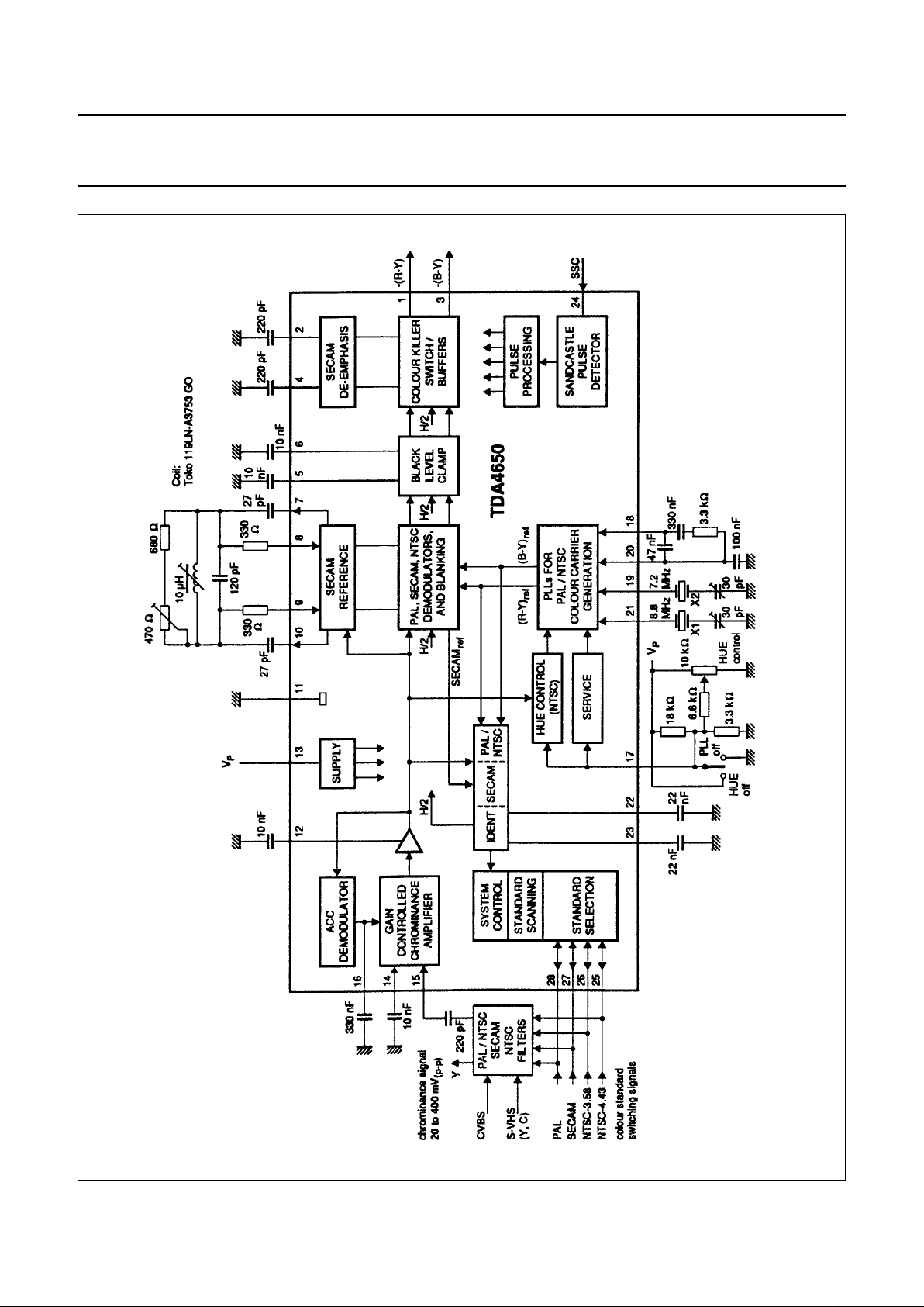
Fig.1 Block diagram.
March 1991 4
Philips Semiconductors Preliminary specification
Multistandard colour decoder, with
negative colour difference output signals
TDA4650
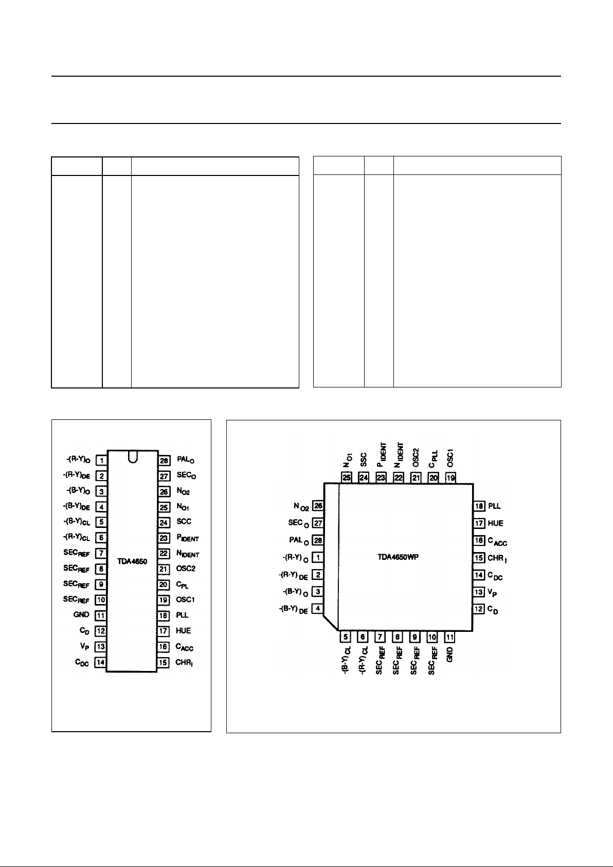
PINNING
SYMBOL PIN DESCRIPTION
−(R-Y)
o
1 −(R-Y) output
−(R-Y)
DE
2 (R-Y) de-emphasis
−(B-Y)
o
3 −(B-Y) output
−(B-Y)
DE
4 (B-Y) de-emphasis
−(B-Y)
CL
5 (B-Y) clamping
−(R-Y)
CL
6 (R-Y) clamping
SEC
REF
7 SECAM reference tuned circuit
SEC
REF
8 SECAM reference tuned circuit
SEC
REF
9 SECAM reference tuned circuit
SEC
REF
10 SECAM reference tuned circuit
GND 11 ground
C
D
12 DC for demodulators
V
P
13 supply voltage
C
DC
14 DC feedback
CHR
I
15 chrominance input
C
ACC
16 automatic colour control
HUE 17 hue control
PLL 18 PLL time constant
OSC1 19 input for 7.15 MHz oscillator
C
PLL
20 PLL DC reference
OSC2 21 input for 8.86 MHz oscillator
N
IDENT
22 NTSC identification
P
IDENT
23 PAL/SECAM identification
SSC 24 super sandcastle pulse input
N
O1
25 NTSC (4.43 MHz) identification
N
O2
26 NTSC (3.58 MHz) identification
SEC
o
27 SECAM identification
PAL
o
28 PAL identification
SYMBOL PIN DESCRIPTION
PIN CONFIGURATIONS
Fig.2 Pin configuration for DIL
package
Fig.3 Pin configuration for PLCC package.
 Loading...