

Philips tda4650 DATASHEETS

INTEGRATED CIRCUITS
DATA SH EET
TDA4650
Multistandard colour decoder, with
negative colour difference output
signals
Preliminary specification
File under Integrated Circuits, IC02
March 1991
Philips Semiconductors Preliminary specification
Multistandard colour decoder, with negative
colour difference output signals
FEATURES
Identifies and demodulates PAL,
SECAM, NTSC 3.58 and NTSC 4.43
chrominance signals with:
• Identification
– automatic standard identification
by sequential inquiry
– secure SECAM identification at
50 Hz only, with PAL priority
– four switched outputs for
chrominance filter selection and
display control
– external service switch for
oscillator adjustment
• PAL / NTSC demodulation
– H (burst) and V blanking
– PAL switch (disabled for NTSC)
– NTSC phase shift (disabled for
PAL)
– PLL-controlled reference
oscillator
– two reference oscillator crystals
on separate pins with automatic
switching
– quadrature demodulator with
subcarrier reference
• SECAM demodulation
– limiter-amplifier
– quadrature-demodulator with a
single external reference tuned
circuit
– alternate line blanking, H and V
blanking
– de-emphasis
TDA4650
• Gain controlled chrominance
amplifier
• ACC demodulation controlled by
system scanning
• Internal colour-difference signal
output filters to remove the residual
subcarrier
GENERAL DESCRIPTION
The TDA4650 is a monolitic
integrated multistandard colour
decoder for PAL, SECAM and NTSC
(3.58 and 4.43 MHz) with negative
colour difference output signals. The
colour-difference output signals are
fed to the TDA4660/TDA4661,
Switched capacitor delay line.
QUICK REFERENCE DATA
SYMBOL PARAMETER CONDITIONS MIN. TYP. MAX. UNIT
V
p
I
p
v
i(p-p)
V
o(p-p)
ORDERING INFORMATION
TYPE NUMBER
TDA4650 28 DIL plastic SOT117
TDA4650WP 28 PLCC plastic SOT261
supply voltage range (pin 13) 10.8 12.0 13.2 V
supply current
(pin 13)
chrominance input voltage (pin 15)
(peak-to-peak value)
colour-difference output voltage (pin 1)
(peak-to-peak value)
colour-difference output voltage (pin 3)
(peak-to-peak value)
colour-difference output voltage (pin 1)
(peak-to-peak value)
colour-difference output voltage (pin 3)
(peak-to-peak value)
EXTENDED
PINS PIN POSITION MATERIAL CODE
PAL/NTSC 0.42 0.525 0.66 V
PAL/NTSC 0.53 0.665 0.84 V
SECAM 0.83 1.05 1.32 V
SECAM 1.06 1.33 1.67 V
PACKAGE
− 60 − mA
20 100 400 mV
(1)
(2)
Note
1. SOT117-1; 1996 November 28.
2. SOT261-2; 1996 November 28.
March 1991 2
Philips Semiconductors Preliminary specification
Multistandard colour decoder, with
negative colour difference output signals
TDA4650
March 1991 3
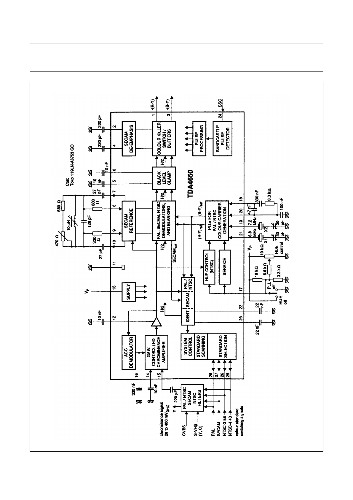
Fig.1 Block diagram.
Philips Semiconductors Preliminary specification
Multistandard colour decoder, with
negative colour difference output signals
PINNING
SYMBOL PIN DESCRIPTION
−(R-Y)
−(R-Y)
−(B-Y)
−(B-Y)
−(B-Y)
−(R-Y)
SEC
REF
SEC
REF
SEC
REF
SEC
REF
GND 11 ground
C
D
V
P
C
DC
1 −(R-Y) output
o
2 (R-Y) de-emphasis
DE
3 −(B-Y) output
o
4 (B-Y) de-emphasis
DE
5 (B-Y) clamping
CL
6 (R-Y) clamping
CL
7 SECAM reference tuned circuit
8 SECAM reference tuned circuit
9 SECAM reference tuned circuit
10 SECAM reference tuned circuit
12 DC for demodulators
13 supply voltage
14 DC feedback
TDA4650
SYMBOL PIN DESCRIPTION
CHR
C
ACC
HUE 17 hue control
PLL 18 PLL time constant
OSC1 19 input for 7.15 MHz oscillator
C
PLL
OSC2 21 input for 8.86 MHz oscillator
N
IDENT
P
IDENT
SSC 24 super sandcastle pulse input
N
O1
N
O2
SEC
o
PAL
o
15 chrominance input
I
16 automatic colour control
20 PLL DC reference
22 NTSC identification
23 PAL/SECAM identification
25 NTSC (4.43 MHz) identification
26 NTSC (3.58 MHz) identification
27 SECAM identification
28 PAL identification
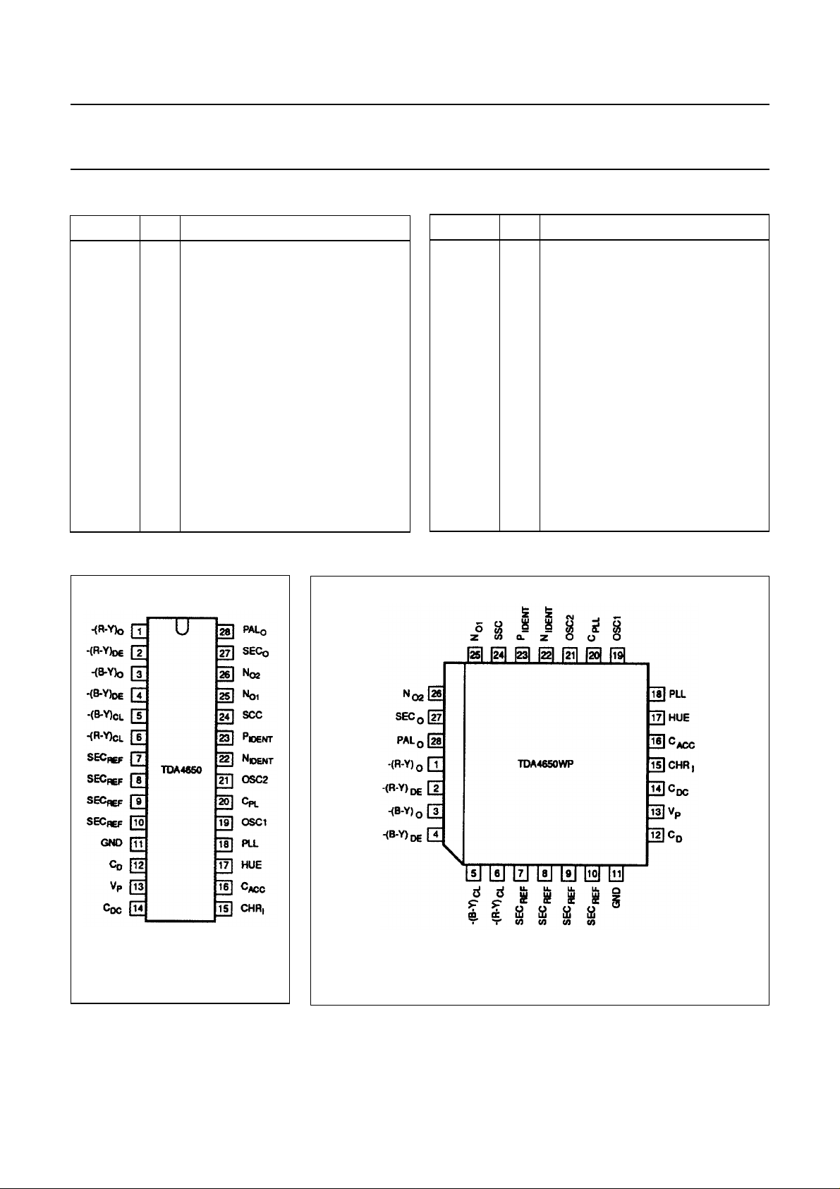
PIN CONFIGURATIONS
Fig.2 Pin configuration for DIL
package
Fig.3 Pin configuration for PLCC package.
March 1991 4
 Loading...