

Philips TDA3856T, TDA3856 Datasheet

INTEGRATED CIRCUITS
DATA SH EET
TDA3856
Quasi-split sound processor for all
standards
Product specification
File under Integrated Circuits, IC02
June 1994
Philips Semiconductors Product specification
Quasi-split sound processor for all standards TDA3856
FEATURES
• Quasi-split sound processor for all standards e. g. B/G (FM sound) and L (AM sound)
• Automatic muting of the AF2 signal (at B/G) by the input level
• AM signal processing for L standard and switching over the audio signal
• Layout-compatible with TDA3858 (32 pins) and TDA3857 (20 pins).
GENERAL DESCRIPTION
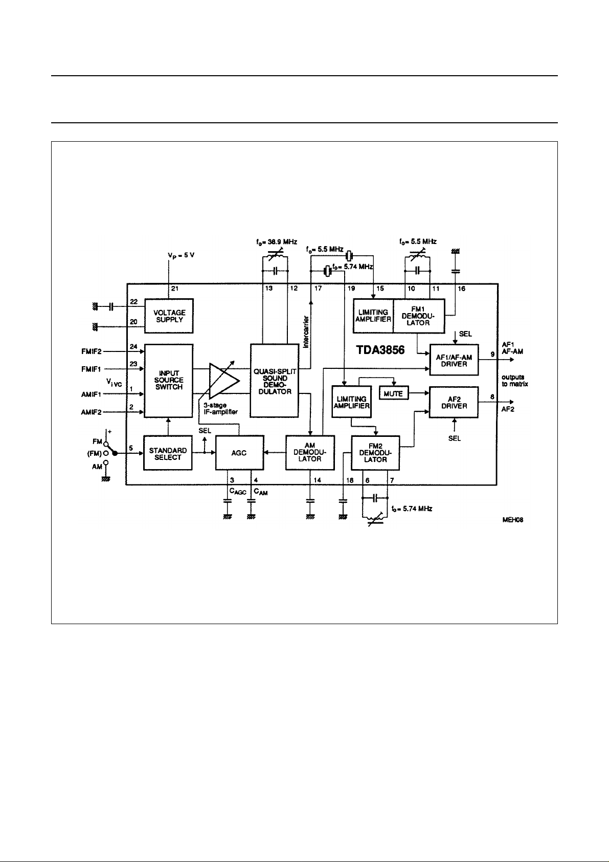
Separate symmetrical IF inputs for FM or AM sound.
Gain controlled wideband IF amplifier, input select switch. AGC generation due to peak sync for FM or mean signal level
for AM. Reference amplifier for the regeneration of the vision carrier. Optimized limiting amplifier for AM suppression in
the regenerated vision carrier signal and 90° phase shifter. Intercarrier mixer for FM sound, output with low-pass filter.
Separate signal processing for 5.5 and 5.74 MHz intercarriers. Wide supply voltage range, only 300 mW power
dissipation at 5 V.
QUICK REFERENCE DATA
SYMBOL PARAMETER MIN. TYP. MAX. UNIT
V
P
I
P
V
i IF
V
o(RMS)
V
o(RMS)
supply voltage (pin 21) 4.5 5 8.8 V
supply current − 60 72 mA
IF input sensitivity (−3 dB) − 70 100 µV
audio output signal for FM (B/G) − 1 − V
audio output signal for AM (L) − 0.6 − V
THD total harmonic distortion
for FM − 0.5 − %
for AM − 1 − %
S/N (W) weighted signal-to-noise ratio
for FM − 68 − dB
for AM − 56 − dB
ORDERING INFORMATION
PACKAGE
EXTENDED
TYPE NUMBER
PINS
PIN
POSITION
MATERIAL CODE
TDA3856 24 shrink DIL plastic SOT234
TDA3856T 24 SO plastic SOT137
(1)
(2)
Note
1. SOT234-1; 1996 November 28.
2. SOT137-1; 1996 November 28.
June 1994 2
Philips Semiconductors Product specification
Quasi-split sound processor for all standards TDA3856
Fig.1 Block diagram (B/G and L).
June 1994 3
Philips Semiconductors Product specification
Quasi-split sound processor for all standards TDA3856
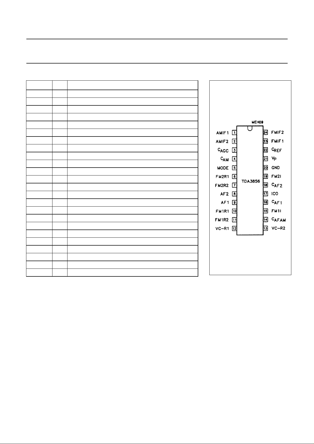
PINNING
SYMBOL PIN DESCRIPTION
AMIF1 1 AM IF difference input 1 for L standard (32.4 MHz)
AMIF2 2 AM IF difference input 2 for L standard (32.4 MHz)
C
AGC
C
AM
MODE 5 3-state input for standard select
FM2R1 6 reference circuit for FM2 (5.74 MHz)
FM2R2 7 reference circuit for FM2 (5.74 MHz)
AF2 8 AF2 output (AF out of 5.74 MHz)
AF1 9 AF1 output (AF out of 5.5 MHz or AM)
FM1R1 10 reference circuit for FM1 (5.5 MHz)
FM1R2 11 reference circuit for FM1 (5.5 MHz)
VC-R1 12 reference circuit for the vision carrier (38.9 MHz)
VC-R2 13 reference circuit for the vision carrier (38.9 MHz)
C
AFAM
FM1| 15 intercarrier input for FM1 (5.5 MHz)
C
AF1
ICO 17 intercarrier output signal (5.5/5.74 MHz)
C
AF2
FM2I 19 intercarrier input for FM2 (5.74 MHz)
GND 20 ground (0 V)
V
P
C
REF
FMIF1 23 IF difference input 1 for B/G standard (38.9 MHz)
FMIF2 24 IF difference input 2 for B/G standard (38.9 MHz)
3 charge capacitor for AGC (FM and AM)
4 charge capacitor for AM AGC
14 DC decoupling capacitor for AM demodulator (AF-AM)
16 DC decoupling capacitor for FM1 demodulator (AF1)
18 DC decoupling capacitor for FM2 demodulator (AF2)
21 +5 to +8 V supply voltage
22 charge capacitor for reference voltage
Fig.2 Pin configuration.
June 1994 4

Philips Semiconductors Product specification
Quasi-split sound processor for all standards TDA3856
FUNCTIONAL DESCRIPTION
The quasi-split sound processor is suitable for all
standards.
Dependent on the voltage at pin 5 either FM mode (B/G)
or AM mode (L) is selected.
B/G standard (FM mode)
Pins 23 and 24 are active, AGC detector uses peak sync
level. Sound carrier SC1 (5.5 MHz) provides AF1, sound
carrier SC2 (5.74 MHz) provides AF2.
Muting
With no sound carrier SC2 at pin 19, AF2 output is muted
(in mid-position of the standard select switch FM mode
without muting of AF2 is selected).
The mute circuit prevents false signal recognition in the
stereo decoder at high IF signal levels when no second
sound carrier exists (mono) and an AF signal is present in
the identification signal frequency range.
With 1 mV at pin 19, under measurement conditions, AF2
is switched on (see limiting amplifier). Weak input signals
at pins 23 and 24 generate noise at pin 19, which is
present in the intercarrier signal and passes through the
5.74 MHz filter. Noise at pin 19 inhibits muting. No
misinterpretation due to white noise occurs in the stereo
decoder, when non-correlated noise masks the
identification signal frequencies, which may be present in
sustained tone signals. The stereo decoder remains
switched to mono.
L standard (AM mode)
Pins 1 and 2 are active, AGC detector uses mean signal
level. The audio signal from the AM demodulator is output
on AF1, with AF2 output muted.
Sound carrier notch filter for an improved intercarrier
buzz
The series capacitor C
in the 38.9 MHz resonant circuit
s
provides a notch at the sound carrier frequency in order to
provide more attenuation for the sound carrier in the vision
carrier reference channel. The ratio of parallel/series
capacitor depends on the ratio of VC/SC frequency and
has to be adapted to other TV transmission standards if
necessary, according to the formula Cs= CP(fvc/fsc)2− CP.
The result is an improved intercarrier buzz (up to 10 dB
improvement in sound channel 2 with 250 kHz video
modulation for B/G stereo) or suppression of 350 kHz
video modulated beat frequency in the digitally-modulated
NICAM subcarrier.
Intercarrier buzz fine tuning with 250 kHz square
wave video modulation
The picture carrier for quadrature demodulation in the
intercarrier mixer is not exactly 90 degrees due to the shift
variation in the integrated phase shift network. The tuning
of the LC reference circuit to provide optimal video
suppression at the intercarrier output is not the same as
that to provide optimal intercarrier buzz suppression. In
order to optimize the AF signal performance, a fine tuning
for the optimal S/N at the sound channel 2 (from 5.74 MHz)
may be performed with a 250 kHz square wave video
modulation.
Measurements at the demodulators
For all signal-to-noise measurements the generator must
meet the following specifications: phase modulation
errors < 0.5° for B/W-jumps
intercarrier signal-to-noise ratio as measured with
‘TV-demodulator AMF2’ (weighted S/N) must be > 60 dB
at 6 kHz sine wave modulation of the B/W-signal.
Signal-to-noise ratios are measured with ∆f=±50 kHz
deviation and f
= 1 kHz; with a deviation of ±30 kHz the
mod
S/N ratio is deteriorated by 4.5 dB.
June 1994 5
Philips Semiconductors Product specification
Quasi-split sound processor for all standards TDA3856
LIMITING VALUES
In accordance with the Absolute Maximum Rating System (IEC 134).
SYMBOL PARAMETER MIN. MAX. UNIT
V
P1
V
I
P
tot
T
stg
T
amb
V
ESD
Note to the Limiting Values
1. Equivalent to discharging a 200 pF capacitor through a 0 Ω series resistor.
supply voltage (pin 21) − 8.8 V
voltage (pins 1, 2, 5, 8, 9, 15, 17, 19, 23 and 24) 0 V
P
V
total power dissipation 0 650 mW
storage temperature −25 +150 °C
operating ambient temperature 0 +70 °C
electrostatic handling (note 1)
all pins except pins 1, 2, 23 and 24 ±500 − V
pins 1, 2, 23 and 24 +400 − V
−500 − V
CHARACTERISTICS
= 5 V and T
V
P
f
= 33.158 MHz. Vision carrier (VC) modulated with different video signals, modulation depth 100% (proportional to
SC2
= +25 °C; measurements taken in Fig.3 with fvc= 38.9 MHz, f
amb
= 33.4 MHz and
SC1
10% residual carrier).
Vision carrier amplitude (RMS value) V
= 10 mV; vision to sound carrier ratios are VC/SC1 = 13 dB and
iVC
VC/SC2 = 20 dB. Sound carriers (SC1, SC2) modulated with f = 1 kHz and deviation ∆f = 50 kHz, unless otherwise
specified.
SYMBOL PARAMETER CONDITIONS MIN. TYP. MAX. UNIT
V
P
I
P
supply voltage (pin 21) 4.5 5 8.8 V
supply current (pin 21) 48 60 72 mA
IF source control (pin 5)
V
5
input voltage in order to obtain standards
B/G (FM) with automatic muting pin 5 connected 2.8 − V
V
P
pin 5 open-circuit − 2.8 − V
B/G (FM) without muting pin 5 connected or
1.3 − 2.3 V
alternative measure:
22 kΩ to GND
L (AM sound) pin 5 connected 0 − 0.8 V
I
5
input current V5=V
V
=0 V −−−300 µA
5
P
−−100 µA
IF input not activated (pins 1-2 or 23-24)
R
V
α
I
I
12-13
input resistance −−100 Ω
DC input voltage (pins 1, 2 or 23, 24) LOW set internally −−0.1 V
crosstalk attenuation of IF input switch note 1 50 56 − dB
IF amplifier (pins 1-2 or 23-24)
R
I
C
I
input resistance 1.8 2.2 − kΩ
input capacitance − 2.0 2.6 pF
June 1994 6
 Loading...