

Philips TDA3845 Service Manual

INTEGRATED CIRCUITS
DATA SH EET
TDA3845; TDA3845T
Quasi split-sound circuit and AM
demodulator
Objective specification
File under Integrated Circuits, IC02
January 1993

Philips Semiconductors Objective specification
Quasi split-sound circuit and AM
TDA3845; TDA3845T
demodulator
FEATURES
• Power supply from 5 V (200 mW) to 8 V source also an
alternative 12 V source (12 V not for TDA3845T)
• Gain controlled wideband IF amplifier (AC coupled with
three stages)
• High precision internal 90° phase shifter for quadrature
demodulator
• Amplitude detector for gain control which operates as a
peak detector for FM sound and as a mean level
detector for AM sound (switchable)
• In-phase wideband synchronous demodulator for AM
detection
QUICK REFERENCE DATA
SYMBOL PARAMETER MIN. TYP. MAX. UNIT
positive supply voltage
V
P1
V
P2
I
P
V
1-16(RMS)
pin 14 4.5 5.0 8.8 V
pin 11 (not for TDA3845T) 10.8 12.0 13.2 V
supply current − 40 − mA
minimum IF input voltage (RMS value) − 70 100 µV
IF control range 60 63 − dB
V
12-13(RMS)
intercarrier output voltage 5.5 MHz (RMS value) 70 100 − mV
(S +W)/W signal-to-weighted-noise ratio
(relative to 1 kHz; 50 kHz deviation)
at 5.5 MHz for 2T/20T − 60 − dB
at 5.742 MHz for 2T/20T − 58 − dB
V
6-13(RMS)
AF output voltage AM (RMS value) 440 550 660 mV
(S +W)/W signal-to-weighted-noise ratio; AM mode − 56 − dB
THD total harmonic distortion; AM mode − 12%
T
amb
operating ambient temperature 0 − +70 °C
• Stabilizer circuit for ripple rejection and constant output
signals
• ESD protection for all pins
• Suitable for all FM standards and L as well as L-accent
standard
• NICAM compatible.
GENERAL DESCRIPTION
The TDA3845 is a quasi split-sound IF circuit which is
designed to provide high performance television FM/AM
sound.
ORDERING INFORMATION
EXTENDED
TYPE NUMBER
PINS PIN POSITION MATERIAL CODE
PACKAGE
TDA3845 16 DIL plastic SOT38
TDA3845T 16 SO16 plastic SOT109A
Note
1. SOT38-1; 1996 November 28.
2. SOT109-1; 1996 November 28.
January 1993 2
(1)
(2)

Philips Semiconductors Objective specification
Quasi split-sound circuit and AM
demodulator
TDA3845; TDA3845T
(1) See note 10 to the characteristics.
(2) Not for TDA3845T, pin 11 not connected.
Fig.1 Block diagram.
January 1993 3
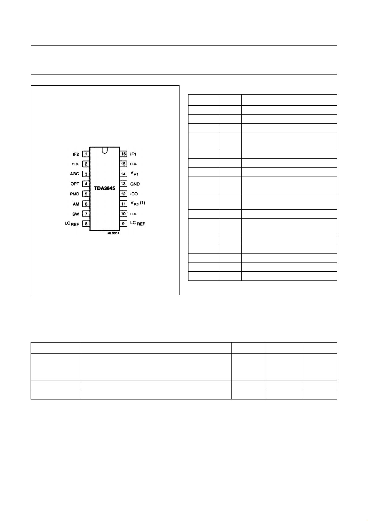
Philips Semiconductors Objective specification
Quasi split-sound circuit and AM
demodulator
(1) not for TDA3845T, pin 11 not connected.
Fig.2 Pin configuration.
TDA3845; TDA3845T
PINNING
SYMBOL PIN DESCRIPTION
IF2 1 IF amplifier input 2
n.c. 2 not connected
AGC 3 AGC control capacitor
OPT 4 optional capacitor (see note 10 to
the characteristics)
PMD 5 peak/mean detector capacitor
AM 6 AM output
SW 7 FM/AM switch
LC
REF
LC
REF
n.c. 10 not connected
V
P2
ICO 12 intercarrier output
GND 13 ground (0 V)
V
P1
n.c. 15 not connected
IF1 16 IF amplifier input 1
Note to Pinning
1. Not for TDA3845T, pin 11 not connected.
8 LC reference circuit for the picture
carrier
9 LC reference circuit for the picture
carrier
11 positive supply voltage 2
(+12 V); note 1
14 positive supply voltage 1 (+5 V)
LIMITING VALUES
In accordance with the Absolute Maximum Rating System (IEC134)
SYMBOL PARAMETER MIN. MAX. UNIT
supply voltage
V
P1
V
P2
T
amb
T
stg
pin 14 4.5 8.8 V
pin 11 (not for TDA3845T) 10.8 13.2 V
operating ambient temperature 0 +70 °C
storage temperature −25 +125 °C
January 1993 4

Philips Semiconductors Objective specification
Quasi split-sound circuit and AM
TDA3845; TDA3845T
demodulator
CHARACTERISTICS
= 5 V (note 11); T
V
P1
SYMBOL PARAMETER CONDITIONS MIN. TYP. MAX. UNIT
Supply
supply voltage
V
P1
V
P2
I
tot
pin 14 4.5 5.0 8.8 V
pin 11 (not for TDA3845T) 10.8 12.0 13.2 V
total supply current − 40 48 mA
IF amplifier
R
1-16
C
1-16
V
1-16(RMS)
input resistance − 2 − kΩ
input capacitance − 2.5 − pF
minimum IF input voltage
(RMS value)
V
1-16(RMS)
maximum IF input voltage
(RMS value)
∆G gain control range 60 63 − dB
G
B
V
v3-16
IF
1-16
gain control voltage range 1.5 − 3.0 V
IF bandwidth −3 dB 50 70 − MHz
DC potential − 1.7 − V
Intercarrier mode (FM mode; standard B/G) notes 3, 4 and 5
Reference amplifier
V
8-9(p-p)
picture carrier amplitude
(peak-to-peak value)
R
8-9
V
8-9
operating resistance − 4 − kΩ
DC potential − 3.9 − V
Intercarrier mixer and output stage
V
12(RMS)
output signal (RMS value)
at 5.5 MHz 70 100 − mV
at 5.74 MHz 32 45 − mV
B
12
intercarrier bandwidth
at −1 dB − 8 − MHz
at −3 dB − 9 − MHz
residual video AM on intercarrier
signal
R
12
V
12
I
12(peak)
output resistance − 30 −Ω
DC potential − 1.8 − V
permissible AC output current
(peak value)
I
12
permissible DC output current −−−2mA
= 25 °C; all measurements are referenced to ground (pin 13); unless otherwise specified.
amb
note 1 − 70 100 µV
note 2 70 100 − mV
− 270 − mV
note 6 − 310%
note 7 −−±0.7 mA
January 1993 5

Philips Semiconductors Objective specification
Quasi split-sound circuit and AM
TDA3845; TDA3845T
demodulator
SYMBOL PARAMETER CONDITIONS MIN. TYP. MAX. UNIT
AF signal performance (note 8)
(S +W)/W black picture 60/58 68/64 − dB
(S +W)/W 2T/20T pulses with white bars 57/55 60/58 − dB
(S +W)/W 6 kHz sinewave
(black-to-white modulation)
(S +W)/W 250 kHz square wave
(black-to-white modulation)
AM mode (standard L) note 9
S/N weighted in accordance with CCIR 468-3
V
6(RMS)
B
AF
AF output signal (RMS value) 440 550 660 mV
AF bandwidth −3 dB; note 12 0.02 − 120 kHz
THD total harmonic distortion − 12%
(S +W)/W signal-to-weighted-noise ratio note 10 50 56 − dB
R
6
V
6
I
6(peak)
output resistance − 200 −Ω
DC potential − 1.8 − V
permissible AC output current
note 7 −−±0.3 mA
(peak value)
I
6
permissible DC output current −−−1mA
Standard switch (note 4)
V
7
V
7
V
7
I
7
peak signal AGC (FM mode) VP1 used 1.8 − V
or switch open-circuit VP2 used 1.8 − 5.5 V
mean signal AGC (AM mode) −−0.8 V
switch current
at 0 V −−−200 µA
at V
P1
at V
P2
via a 2.2 kΩ series resistor −−2.5 mA
Ripple rejection (note 13)
AM/AF signal
αRR voltage ripple on V
/
P
voltage ripple on output signal
FM phase noise
∆f(RMS) intercarrier signal − 10 20 Hz
53/51 57/55 − dB
50/44 56/50 − dB
P1
V
−−10 µA
30 40 − dB
January 1993 6
 Loading...