


INTEGRATED CIRCUITS
DATA SH EET
TDA1388
Bitstream continuous calibration
filter-DAC for CD-ROM audio
applications
Objective specification
Supersedes data of 1995 Dec 08
File under Integrated Circuits, IC01
1996 Jul 17

Philips Semiconductors Objective specification
Bitstream continuous calibration filter-DAC
for CD-ROM audio applications
FEATURES
Multiple format input interface
2
• I
S-bus and LSB-justified input format compatible
• 1fs input format data rate.
Extensive channel manipulation features
• Separate soft mute on left and right channel
• Channel interchange function (left to right and right to
left)
• Monaural function (left to right or right to left)
1
• True mono function
Digital sound processing
• Separate digital volume control for left and right
channels
• Digital tone control, bass boost and treble
• dB-linear volume and tone control (low microcontroller
load)
• Digital de-emphasis
• Soft mute.
Advanced audio output configuration
• Stereo line output (under microcontroller volume
control)
• Stereo headphone output (under 5-tap potentiometer
volume control)
• Line output independent of headphone output volume
• Power on/off click prevention circuitry
• High linearity, dynamic range, low distortion.
General
• Integrated digital filter plus DAC plus headphone driver
• No analog post filter required
• Easy application
• Functions controllable by static pins or by
microcontroller interface
• 5 V power supply
• Low power consumption
• Small package size (SO28 and SSOP28).
⁄2(left plus right).
GENERAL DESCRIPTION
The TDA1388 CMOS digital-to-analog bitstream converter
incorporates an up-sampling digital filter and noise shaper,
unique signal processing features and integrated line and
headphone drivers. The digital processing features are of
high sound quality due to the wide dynamic range of the
bitstream conversion technique.
The TDA1388 supports the I
word lengths of up to 20 bits and the LSB justified serial
data input format with word lengths of 16, 18 and 20 bits.
Two cascaded half-band filters and a sample-and-hold
function increase the oversampling rate from 1f
A 2nd-order noise shaper converts this oversampled data
to a bitstream for the 5-bit continuous calibration
Digital-to-Analog Converters (DACs).
On board amplifiers convert the output current to a voltage
signal capable of driving a line output. The signal is also
used to feed the integrated headphone amplifiers.
The volume of the headphone is controlled by an external
potentiometer.
The TDA1388 has special sound processing features for
use in CD-ROM audio applications, which can be
controlled by static pins or microcontroller interface.
These functions are de-emphasis, volume, bass boost,
treble, soft mute and the channel manipulation functions
needed for ATAPI-compliant functionality in CD-ROM
audio processing.
TDA1388
2
S-bus data input mode with
to 64fs.
s
1996 Jul 17 2
Philips Semiconductors Objective specification
Bitstream continuous calibration filter-DAC
TDA1388
for CD-ROM audio applications
ORDERING INFORMATION
= 256f
= 384f
PACKAGE
s
s
−−85 −80 dB
− 0.006 0.013 %
−−35 −30 dBA
− 1.8 3.2 %
−−65 − dB
− 0.056 − %
−−70 − dB
− 0.032 − %
−−35 −30 dBA
− 1.8 3.2 %
90 95 − dBA
− 64f
− 48f
s
s
− bits
− bits
TYPE
NUMBER
NAME DESCRIPTION VERSION
TDA1388T SO28 plastic small outline package; 28 leads; body width 7.5 mm. SOT136-1
TDA1388M SSOP28 plastic shrink small outline package; 28 leads; body width 5.3 mm. SOT341-1
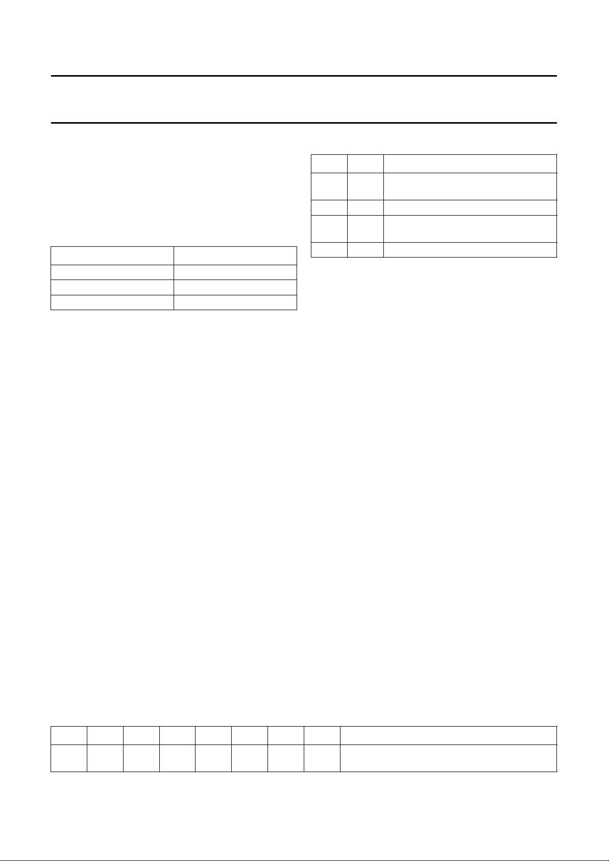
QUICK REFERENCE DATA
SYMBOL PARAMETER CONDITIONS MIN. TYP. MAX. UNIT
Supply
V
DD
I
DD
V
FS(rms)
supply voltage note 1 4.5 5.0 5.5 V
supply current note 2 − 22 − mA
full-scale output voltage
VDD= 5 V 0.9 1.0 1.1 V
(RMS value)
(THD+N)/S total harmonic distortion plus
noise as a function of signal for
the line output
total harmonic distortion plus
noise as a function of signal for
the headphone output
0 dB signal;
=5kΩ
R
L
−60 dB signal;
=5kΩ
R
L
0 dB signal;
=16Ω
R
L
0 dB signal;
=32Ω
R
L
−60 dB signal;
=16Ω or RL=32Ω
R
L
S/N signal-to-noise ratio A-weighted;
at code 00000H
BR input bit rate at data input f
f
sys
T
amb
system clock frequency 8.192 − 18.432 MHz
operating ambient temperature −20 − +70 °C
sys
f
sys
Notes
1. All V
and VSS pins must be connected to the same supply or ground respectively.
DD
2. Measured at input code 00000H and VDD=5V.
1996 Jul 17 3
Philips Semiconductors Objective specification
Bitstream continuous calibration filter-DAC
for CD-ROM audio applications
BLOCK DIAGRAM
DATA
IF2
IF1
11
8
7
SERIAL DATA INPUT
SYSCLK
SYSSEL
TC
V
DDD
V
SSD
FILTCL
14
15
20
12
13
5
TIMING
TDA1388
R
CONV1
16 (4-BIT)
CALIBRATED
CURRENT
SOURCES
CHANNEL INTERCHANGE
DE-EMPHASIS
VOLUME CONTROL
BASS BOOST AND TREBLE
SOFT MUTE
FILTER STAGE 1 + 2
SAMPLE-AND-HOLD
16 × OVERSAMPLING
2nd-ORDER
NOISE
SHAPER
DATA
ENCODER
2nd-ORDER
NOISE
SHAPER
DATA
ENCODER
BCK
9
4f
s
64f
s
CALIBRATED
16 (4-BIT)
CURRENT
SOURCES
ACPWS
1910
FEATURE
CONTROL
UNIT
R
CONV2
TDA1388
18
APPL2
17
APPL1
16
APPL0
22
V
DDA
23
V
SSA
24
FILTCR
−
V
OL
V
ref
HPINL
4
V
DDA
6
3
30 kΩ
+
+
−
30 kΩ
LEFT OUTPUT
SWITCHES
16 (4-BIT)
CALIBRATED
CURRENT
SINKS
2
HPOUTL
REFERENCE
SOURCE
REFERENCE
SOURCE
Fig.1 Block diagram.
1996 Jul 17 4
RIGHT OUTPUT
SWITCHES
16 (4-BIT)
CALIBRATED
CURRENT
SINKS
30 kΩ
27
HPOUTR
−
+
+
−
30 kΩ
25
28
21
26
MGD015
V
OR
V
DDO
1
V
SSO1
V
SSO2
HPINR
Philips Semiconductors Objective specification
Bitstream continuous calibration filter-DAC
for CD-ROM audio applications
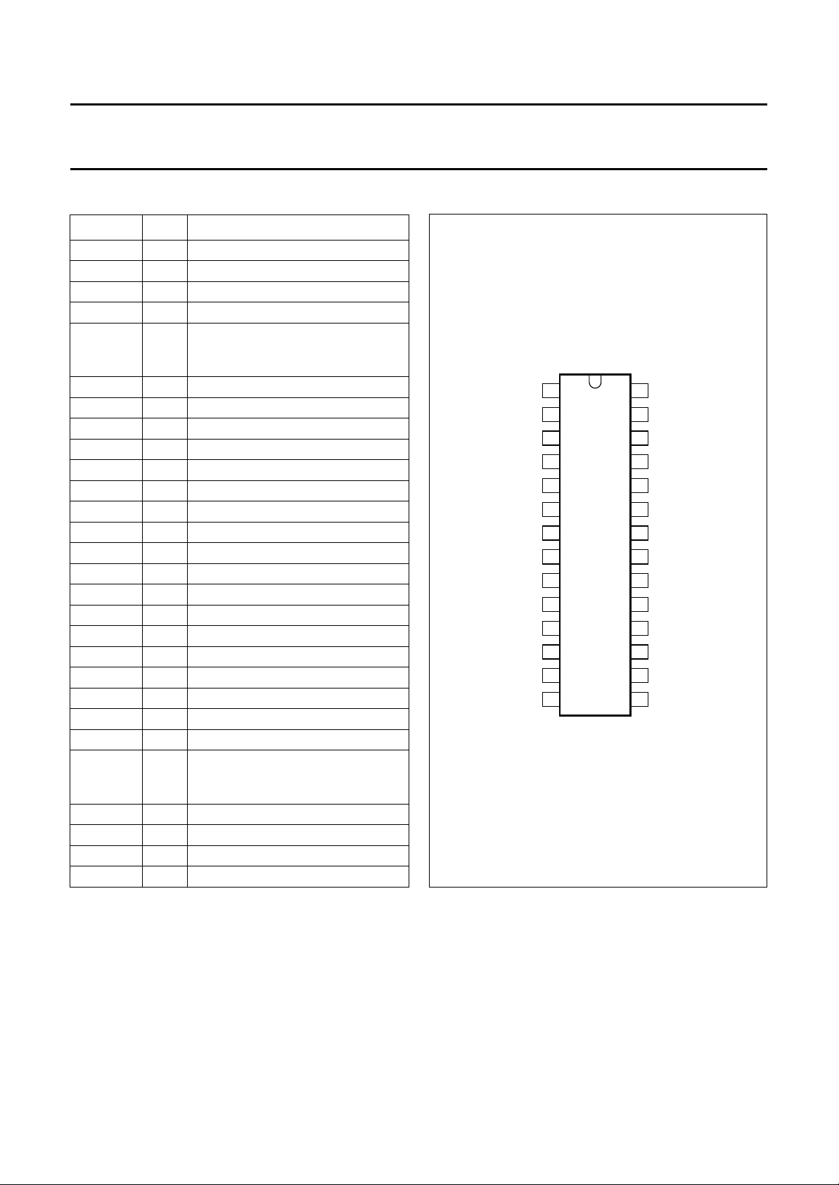
PINNING
SYMBOL PIN DESCRIPTION
V
SSO1
HPOUTL 2 left headphone output voltage
HPINL 3 left headphone input voltage
V
OL
FILTCL 5 capacitor for left channel 1st-order
V
ref
IF1 7 input format selection 1
IF2 8 input format selection 2
BCK 9 bit clock input
WS 10 word selection input
DATA 11 data input
V
DDD
V
SSD
SYSCLK 14 system clock 256f
SYSSEL 15 system clock selection
APPL0 16 application mode 0 input
APPL1 17 application mode 1 input
APPL2 18 application mode 2 input
ACP 19 application control input
TC 20 test control
V
SSO2
V
DDA
V
SSA
FIL TCR 24 capacitor for right channel 1st-order
V
OR
HPINR 26 right headphone input voltage
HPOUTR 27 right headphone output voltage
V
DDO
1 operational amplifier ground 1
4 left channel audio voltage output
filter function, should be connected
between this pin and V
(pin 4)
OL
6 internal reference voltage
12 digital supply voltage
13 digital ground
or 384f
s
s
21 operational amplifier ground 2
22 analog supply voltage
23 analog ground
filter function, should be connected
between this pin and V
(pin 25)
OR
25 right channel audio voltage output
28 operational amplifier supply voltage
handbook, halfpage
V
HPOUTL
FILTCL
SSO1
HPINL
V
OL
V
ref
IF1
1
2
3
4
5
6
7
TDA1388
IF2
8
BCK
9
WS
10
DATA
11
V
12
DDD
V
13
SSD
SYSCLK
14
Fig.2 Pin configuration.
MGD014
TDA1388
V
28
DDO
27
HPOUTR
26
HPINR
25
V
OR
24
FILTCR
23
V
SSA
22
V
DDA
21
V
SSO2
TC
20
ACP
19
APPL2
18
APPL1
17
APPL0
16
SYSSEL
15
1996 Jul 17 5
Philips Semiconductors Objective specification
Bitstream continuous calibration filter-DAC
for CD-ROM audio applications
FUNCTIONAL DESCRIPTION
The TDA1388 CMOS DAC incorporates an up-sampling
digital filter, a sample-and-hold register, a noise shaper,
continuously calibrated current sources, line amplifiers
and headphone amplifiers. The 1fs input data is increased
to an oversampled rate of 64fs. This high-rate
oversampling, together with the 5-bit DAC, enables the
filtering required for waveform smoothing and out-of-band
noise reduction to be achieved by simple 1st-order analog
post-filtering.
System clock
The TDA1388 accommodates slave mode only, this
means that in all applications the system devices must
provide the system clock. The system frequency is
selectable. The options are 256f
clock must be locked in frequency to the I2S-bus input
signals.
Table 1 System clock selection
SYSSEL DESCRIPTION
0 256f
1 384f
Multiple format input interface
The TDA1388 supports the following data input formats;
2
S-bus with data word length of up to 20 bits.
• I
• LSB justified serial format with data word length of
16, 18 or 20 bits.
and 384fs. The system
s
s
s
TDA1388
Table 2 Data input formats
IF1 IF2 FORMAT
2
00I
0 1 LSB-justified, 16 bits
1 0 LSB-justified, 18 bits
1 1 LSB-justified, 20 bits
The input formats are illustrated in Fig.3. Left and right
data-channel words are time multiplexed.
Input mode
The TDA1388 has two input modes, a static-pin mode and
a microcontroller mode. In the static-pin mode, the digital
sound processing features such as mute left, mute right
and de-emphasis are controlled by external pins.
The other digital sound processing features have a default
value. In the microcontroller mode, all the digital sound
processing features can be controlled by the
microcontroller. The controllable features are:
• De-emphasis
• Volume left channel
• Volume right channel
• Flat/min/max switch
• Bass boost
• Treble
• Channel manipulation modes.
The selection of one of the two modes is controlled by the
ACP pin. When this pin is at logic 0 then the static pin
mode will be selected. When the pin is at logic 1 then the
microcontroller mode will be selected.
S-bus
Table 3 Selectable values of the digital sound processing features
FEATURES STATIC-PIN MODE MICROCONTROLLER MODE
De-emphasis 0 Hz or 44.1 kHz 0 Hz or 44.1 kHz
Volume left channel 0 dB (fixed) 0 dB to −∞ dB
Volume right channel 0 dB (fixed) 0 dB to −∞ dB
Flat/min/max switch flat (fixed) flat/min/max
Bass boost flat set (fixed) flat, min or max set
Treble flat set (fixed) flat, min or max set
Mute left channel external pin selectable (see Table 4)
Mute right channel external pin selectable (see Table 4)
Channel manipulation modes L_CHANNEL = L (fixed) selectable (see Table 10)
R_CHANNEL = R (fixed)
1996 Jul 17 6
Philips Semiconductors Objective specification
Bitstream continuous calibration filter-DAC
for CD-ROM audio applications
STATIC-PIN MODE
In the static-pin mode most of the features have a default
value (see Table 3). The features that are controlled by the
external pins are, mute left channel, mute right channel
and de-emphasis.
Table 4 External pin feature control in the static-pin
mode
PIN FEATURE
APPL0 mute left channel
APPL1 mute right channel
APPL2 de-emphasis
ICROCONTROLLER MODE
M
The exchange of data and control information between the
microcontroller and the TDA1388 is accomplished through
a serial hardware interface comprising the following pins:
APPL0: microcontroller interface data line.
APPL1: microcontroller interface mode line.
APPL2: microcontroller interface clock line.
Information transfer through the microcontroller bus is
organized in accordance with the so-called ‘L3’ format, in
which two different modes of operation can be
distinguished; address mode and data transfer mode
(see Figs 4 and 5).
TDA1388
Table 5 Selection of data transfer
BIT 1 BIT 0 TRANSFER
0 0 data (volume left, volume right, bass
boost and treble)
0 1 not used
1 0 status (de-emphasis, mode and
channel-manipulation)
1 1 not used
Data bits 7 to 2 represent a 6-bit device address, with bit 7
being the MSB and bit 2 the LSB. The address of the
TDA1388 is 000101 (bit 7 to bit 2). In the event that the
TDA1388 receives a different address, it will deselect its
microcontroller interface logic.
Data transfer mode
The selection preformed in the address mode remains
active during subsequent data transfers, until the
TDA1388 receives a new address command.
The fundamental timing of data transfers is essentially the
same as in the address mode, shown in Fig.4.
The maximum input clock and data rate is 64fs. All
transfers are bitwise, i.e. they are based on groups of
8 bits. Data will be stored in the TDA1388 after the eighth
bit of a byte has been received. A multibyte transfer is
illustrated in Fig.6.
The address mode is required to select a device
communicating via the L3-bus and to define the
destination registers for the data transfer mode.
Data transfer for the TDA1388 can only be in one direction,
input to the TDA1388 to program its sound processing and
other functional features.
Address mode
The address mode is used to select a device for
subsequent data transfer and to define the destination
registers. The address mode is characterized by APPL1
being LOW and a burst of 8 pulses on APPL2,
accompanied by 8 data bits. The fundamental timing is
shown in Fig.4. Data bits 0 to 1 indicate the type of the
subsequent data transfer as shown in Table 5.
Table 6 Data transfer of type ‘status’
BIT 7 BIT6 BIT 5 BIT 4 BIT 3 BIT 2 BIT 1 BIT 0 REGISTER SELECTED
0 M1 M0 DE OR1 OR0 OL1 OL0 MODE (1 : 0), DEEMPHASIS, CHANNEL_MA-
1996 Jul 17 7
Programming the sound processing and other features
The sound processing and other feature values are stored
in independent registers. The first selection of the registers
is achieved by the choice of data type that is transferred.
This is performed in the address mode, BIT 1 and BIT 0
(see Table 5). The second selection is performed by the
2 MSBs of the data byte (BIT 7 and BIT 6). The other bits
in the data byte (BIT 5 to BIT 0) is the value that is placed
in the selected registers.
When the data transfer of type ‘data’ is selected, the
features VOLUME_R, VOLUME_L, BASS BOOST and
TREBLE can be controlled. When the data transfer of type
‘status’ is selected, the features MODE, DE-EMPHASIS,
CHANNEL_MANIP_R and CHANNEL_MANIP_L can be
controlled.
NIP_R (1 : 0), CHANNEL_MANIP_L (1 : 0)

Philips Semiconductors Objective specification
Bitstream continuous calibration filter-DAC
for CD-ROM audio applications
Table 7 Data transfer of type ‘data’
BIT 7 BIT 6 BIT 5 BIT 4 BIT 3 BIT 2 BIT 1 BIT 0 REGISTER SELECTED
0 0 VR5 VR4 VR3 VR2 VR1 VR0 VOLUME_R (5 : 0)
0 1 VL5 VL4 VL3 VL2 VL1 VL0 VOLUME_L (5 : 0)
(1)
10X
11X
Note
1. X = don’t care.
MODE: a 2-bit value to program the mode of the sound
processing filters of Bass Boost and Treble. There are
three modes: flat, min and max.
Table 8 The flat/min/max switch
MODE 1 MODE 0 FUNCTION
0 0 flat
0 1 min
1 0 min
1 1 max
BB4 BB3 BB2 BB1 BB0 BASS BOOST (4 : 0)
(1)
TR4 TR3 TR2 TR1 TR0 TREBLE (4 : 0)
DE-EMPHASIS: a 1-bit value to enable the digital
de-emphasis filter.
Table 9 De-emphasis
DEEM FUNCTION
0 no de-emphasis
1 de-emphasis, 44.1 kHz
TDA1388
CHANNEL_MANIP_R and CHANNEL_MANIP_L: both are a 2 bit value to program the right or left channel manipulation.
Table 10 Channel manipulation modes
CHANNEL_MANIP_L<1 : 0> CHANNEL_MANIP_R<1 : 0> L_CHANNEL R_CHANNEL
00 00 MUTE MUTE
00 01 MUTE R
00 10 MUTE L
1
00 11 MUTE
⁄2(L+R)
01 00 R MUTE
01 01 R R
01 10 R L
1
01 11 R
⁄2(L+R)
10 00 L MUTE
10 01 L R
10 10 L L
1
10 11 L
11 00
11 01
11 10
11 11
1
⁄2(L + R) MUTE
1
⁄2(L + R) R
1
⁄2(L + R) L
1
⁄2(L + R)
⁄2(L+R)
1
⁄2(L+R)
1996 Jul 17 8
 Loading...