

Philips tda1383 DATASHEETS

INTEGRATED CIRCUITS
DATA SH EET
TDA1383
DCC record/playback amplifier
Preliminary specification
File under Integrated Circuits, IC01
1995 Aug 30

Philips Semiconductors Preliminary specification
DCC record/playback amplifier TDA1383
FEATURES
General
• Single 3 V power supply
• Low standby current consumption
• Internal voltage regulator for improved supply ripple
rejection
• Double-speed DCC record and playback
• Can be applied with all generations of digital processing
ICs
• All gains and settings are software controlled
• Reduced number of external components.
Record part
• Single point main data and AUX data record current
setting
• Reduction of power consumption between current
pulses
• Accurate temperature compensation of the record
current by measuring the tape temperature
• Soft switching of record currents
• Timing compatible with TDA1319T and TDA1381H.
GENERAL DESCRIPTION
The TDA1383 is a single-chip record and playback
amplifier for a Digital Compact Cassette (DCC) tapedeck,
including Analog Compact Cassette (ACC) playback
functions. The device is designed to be used with the
Philips DCC head, type RP410R1/15. All modes of
operation and settings can be controlled by a single serial
input. Application of the TDA1383 provides a small,
versatile, low power and inexpensive DCC front-end.
Playback part
• Low noise amplifiers
• Pre-equalization and anti-aliasing filters
• Automatic gain control of DCC preamplifiers
• Optional recording of auxiliary data during DCC
playback
• Auxiliary data detect after record e.g. to detect end of
tape or ‘head clogging’
• Two amplifiers for ACC equalization
• Control signal for ferro/chrome switches
• Mute for ACC playback
• Music search function during ACC (re)wind (to be
confirmed).
ORDERING INFORMATION
TYPE
NUMBER
TDA1383H LQFP48 plastic low profile quad flat package; 48 leads; body 7 × 7 × 1.4 mm SOT313-2
NAME DESCRIPTION VERSION
PACKAGE
1995 Aug 30 2

Philips Semiconductors Preliminary specification
DCC record/playback amplifier TDA1383
QUICK REFERENCE DATA
=25°C; V
T
amb
DD1=VDD2
SYMBOL PARAMETER CONDITIONS MIN. TYP. MAX. UNIT
V
V
DD1
DD1
supply voltage 1 record part 2.7 3.3 5.5 V
supply voltage 1 record part and
playback part
V
DD2
I
DD1+IDD2
I
stb
I
D
supply voltage 2 playback part 2.7 3.3 5.5 V
supply current DCC record mode;
total standby supply current no clock; note 1 −−50 µA
record current main data
channels 0 to 7
I
AUX
record/erase current auxiliary
data channel
P
T
d(av)
amb
average power dissipation DCC record mode;
operating ambient temperature −30 − +85 °C
= 3.3 V; unless otherwise specified.
note 1 tbf 3.3 5.5 V
ID= 100 mA
DCC playback mode;
= 3 mA
I
sense
ACC playback mode;
I
= 3 mA
sense
see Table 1 10 − 125 mA
ID= 100 mA
DCC playback mode;
=3mA
I
sense
ACC playback mode;
=3mA
I
sense
− 45 60 mA
− 52 68 mA
− 29 38 mA
10 − 153 mA
− 130 − mW
− 150 − mW
− 85 − mW
Note
1. V
Table 1 Maximum record current as a function of V
is not connected to V
DD2
V
DD1
(internal voltage regulator on).
DD1
and record head resistance
DD1
R
=10Ω R
rec
2.7 V 75 90 110
3.3 V 90 110 125
>4 V 125 125 125
1995 Aug 30 3
= 6.5 Ω R
rec
rec
=4Ω
Philips Semiconductors Preliminary specification
DCC record/playback amplifier TDA1383
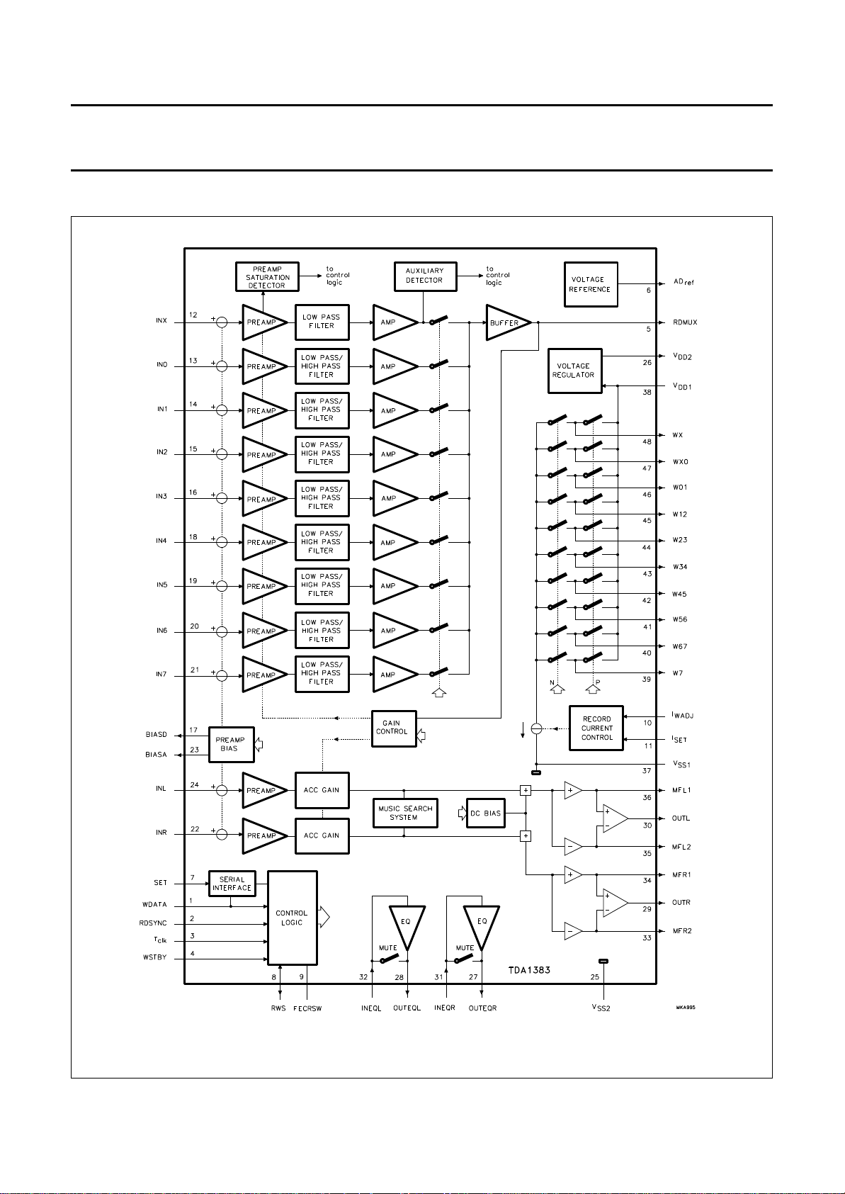
BLOCK DIAGRAM
1995 Aug 30 4
Fig.1 Block diagram.

Philips Semiconductors Preliminary specification
DCC record/playback amplifier TDA1383
PINNING
SYMBOL PIN DESCRIPTION
WDATA 1 record data input/control data input
RDSYNC 2 playback sync input
T
CLK
WSTBY 4 record standby control input
RDMUX 5 multiplexed DCC data output
AD
ref
SET 7 control data input
RWS 8 music search output/AUX detector output/saturation detector output/external clock input
FECRSW 9 ferro-chrome switch control signal
I
WADJ
I
SET
INX 12 auxiliary channel input
IN0 13 channel 0 input
IN1 14 channel 1 input
IN2 15 channel 2 input
IN3 16 channel 3 input
BIASD 17 DCC bias voltage output
IN4 18 channel 4 input
IN5 19 channel 5 input
IN6 20 channel 6 input
IN7 21 channel 7 input
INR 22 ACC right channel input
BIASA 23 ACC bias voltage output
INL 24 ACC left channel input
V
SS2
V
DD2
OUTEQR 27 right channel equalization amplifier output
OUTEQL 28 left channel equalization amplifier output
OUTR 29 right channel ACC output
OUTL 30 left channel ACC output
INEQR 31 right channel equalization amplifier input
INEQL 32 left channel equalization amplifier input
MFR2 33 right channel feedback amplifier output 2
MFR1 34 right channel feedback amplifier output 1
MFL2 35 left channel feedback amplifier output 2
MFL1 36 left channel feedback amplifier output 1
V
SS1
V
DD1
W7 39 channel 7 record current output
W67 40 channel 6/7 record current output
3 tape clock input
6 AD reference voltage output
10 record current adjust input
11 record current set input
25 ground for playback part
26 supply voltage for playback part/voltage regulator output
37 ground for record part (substrate)
38 supply voltage for record part
1995 Aug 30 5

Philips Semiconductors Preliminary specification
DCC record/playback amplifier TDA1383
SYMBOL PIN DESCRIPTION
W56 41 channel 5/6 record current output
W45 42 channel 4/5 record current output
W34 43 channel 3/4 record current output
W23 44 channel 2/3 record current output
W12 45 channel 1/2 record current output
W01 46 channel 0/1 record current output
WX0 47 channel X/0 record current output
WX 48 channel X record current output
1995 Aug 30 6
Fig.2 Pin configuration.

Philips Semiconductors Preliminary specification
DCC record/playback amplifier TDA1383
FUNCTIONAL DESCRIPTION
A brief functional description of each block (see Fig.1) is
given. The record part of the IC includes the record current
control circuit, the current source and output switches. The
DCC playback part includes nine channels, each
consisting of a preamplifier, filters and an amplifier,
automatic gain control and sense current (bias) circuits.
Differential amplifiers with presettable gain and bias are
Modes of operation
All modes and (analog) settings are digitally controlled via
the serial interface. Table 2. shows an overview of the
modes of operation and the corresponding values of the
control bits. For a number of bits it is allowed to deviate
from this table (see description of the control bits). In the
record modes additional control bits must be set, see
Table 11 and Fig.6.
used for ACC feedback to the head.
Table 2 Modes of operation
CONTROL BITS
MODE
DCC playback 0000010
DCC search 0010010 0
DCC playback and AUX
data record
DCC playback and AUX
D6D5D4D3D2D1D0S3S2S1S0G2G1G0B4B3B2B1B
(2)
0
(2)
0000010 0
DCC sense voltage
see Table 11
DCC gain
see Table 12
0110010 0
(2) (2)
(2) (2)
data detection
DCC record 0000110 −−−−−−−1−
(3)
ACC playback 0 0
ACC search 0 1 − 0011 −
Standby
(1)
0000110 −−−−−−−1−−−−
1011
ACC sense voltage
see Table 11
0 DCC gain
see
Table 12
DC bias voltage at
ACC outputs
see Table 10
0
−−−
−−−
−−
−−
(2)
−−
Notes
1. TDAPLB and TAUPLB must be set HIGH (see Table 13).
2. 0 = normal-speed; 1 = double-speed.
3. 0 = LOW level at FECRSW output; 1 = HIGH level at FECRSW output.
Serial interface
Settings of the IC can be programmed either via the SET
input pin or the WDATA input pin. When sending data via
the WDATA pin, the SET pin must be held LOW, the data
is then provided in the SET time-slot of the serial data word
(one bit per cycle of 32 clock periods, see Fig.6). Four
different control bytes are recognised (see Table 3).
The settings can be sent asynchronously at a bit-rate of
1
⁄32f
(96 kbits/s in case of normal speed). The data
Tclk
transfer must be preceeded by a start bit (LOW) and end
with a stop bit (HIGH), as shown in Fig.3. The SET data
detector starts at the falling edge of the start bit. Each
control bit is detected in the middle. After power-up at least
ten stop bits (320 clock periods) must be sent in order to
initialize the serial interface.
Fig.3 Timing diagram of the SET byte.
1995 Aug 30 7
Philips Semiconductors Preliminary specification
DCC record/playback amplifier TDA1383
Table 3 Control bytes
CONTROL BYTE BIT 0 BIT 1 BIT 2 BIT 3 BIT 4 BIT 5 BIT 6 BIT 7
Byte 1 0 0 D0 D1 D2 D3 D4 D5
Byte 2 1 0 D6 − S0 S1 S2 S3
Byte 3 0 1 −−−G1 G1 G2
Byte 4 1 1 − B0 B1 B3 B3 B4
Description of the control bits
Tables 4 to 12 describe the functions of the various control
bits.
The magneto-resistive playback head (MRH) is directly
connected to the IC. Bits D3 to D1 control the internal
Table 4 Control bit D0
D0 MODE
0 DCC playback/record
1 ACC playback
Table 5 Control bits D2 and D1
D2 D1 FUNCTION
0 0 preamp input floating, second stages
normal (for testing only)
0 1 cut-off frequencies normal
1 0 cut-off frequencies high
1 1 cut-off frequencies very high (standby, fast
settling)
Table 8 Detector modes and outputs
AC coupling to the MRH and DC biasing of capacitors
connected between the internal amplifiers (see Fig.9).
The cut-off frequencies are related to the clock frequency
at T
or RWS (bit D3). Higher clock frequencies will result
clk
in higher cut-off frequencies.
Table 6 Control bit D3
D3 FUNCTION
0 cut-off frequencies coupled to the frequency at
T
(pin 3)
clk
1 cut-off frequencies coupled to the frequency at
RWS (pin 8)
Table 7 Control bit D4
D4 DCC MODE (D0 = 0) ACC MODE (D0 = 1)
0 AGC on FECRSW = LOW level
(pin 9)
1 AGC off, gain setting
at G2, G1 and G0
FECRSW = HIGH level
(pin 9)
D5
(1)
D6
FUNCTION IN ACC MODE
0 0 music search detector off AUX detector off control frequency input
0 1 test preamp saturation level test preamp saturation level saturation level detector output
1 0 music search detector on AUX detector on filtered MSS and AUX detector
1 1 music search detector on AUX detector on (direct MSS and AUX detector
Note
1. D3 and D5 should not be at logic 1 at the same time.
1995 Aug 30 8
(D0=1)
FUNCTION IN DCC MODE
(D0=0)
PIN RWS (see Fig.9)
(HIGH when saturated)
output
output, for testing only)
Philips Semiconductors Preliminary specification
DCC record/playback amplifier TDA1383
Table 9 Control bits B4 to B2
BIT VALUE FUNCTION IN DCC MODE (D0 = 0) FUNCTION IN ACC MODE (D0 = 1)
(1)
B4
B3 0 filters set for playback at normal-speed
B2 0 recording at normal-speed
Note
1. The bit B4 determines the sign of feedback bias voltage. If B4 = 0 then MFL1 and MFR1 are negative with respect
to MFL2 and MFR2. If B4 = 1 then MFL1 and MFR1 are positive with respect to MFL2 and MFR2.
Table 10 Feedback conductor bias voltage settings in the ACC mode (D0 = 1, no MRH connected)
0 playback mode on
1 playback mode off
1 filters set for playback at double-speed
1 recording at double-speed
see Table 10
BIAS VOLTAGE BIT
B3 B2 B1 B0
00 0 0 0
00 0 1 30
00 1 0 60
00 1 1 90
0 1 0 0 120
0 1 0 1 150
0 1 1 0 180
0 1 1 1 210
1 0 0 0 240
1 0 0 1 270
1 0 1 0 300
1 0 1 1 330
1 1 0 0 360
1 1 0 1 390
1 1 1 0 420
1 1 1 1 450
TYPICAL DC BIAS VOLTAGE (mV)
1995 Aug 30 9
 Loading...