

Philips tda1380 DATASHEETS

INTEGRATED CIRCUITS
DATA SH EET
TDA1380
DCC read amplifier (READ 3)
Preliminary specification
File under Integrated Circuits, IC01
Philips Semiconductors
September 1994

Philips Semiconductors Preliminary specification
DCC read amplifier (READ 3) TDA1380
FEATURES
• Single 3 V supply
• Low power consumption
• Differential inputs for low power head configuration
• Can be used with 1st, 2nd and 3rd generation digital
signal processing ICs
• Automatic gain control for DCC preamplifiers
• Selectable input amplifiers for A or B side of cassette
• ACC playback via DCC preamplifiers
• Uncommitted amplifiers for equalization during ACC
playback
• Low noise current sources for the sense currents of the
DCC heads
• Generates reference sense current for temperature
compensation of the write current, in recordable
application with the TDA1381
• High feedback application possible (for adjustment
minimization)
• Suitable for digital post-processor.
GENERAL DESCRIPTION
The TDA1380 amplifies, filters and multiplexes signals that
are input from an 18-channel magnetoresistive thin film
head (MRH) suitable for the DCC (Digital Compact
Cassette) and ACC (Analog Compact Cassette) systems.
The device also contains current sources to provide sense
currents through the heads and amplifiers for magnetic
feedback and biasing. Two uncommitted amplifiers are
available for analog equalization.
ORDERING INFORMATION
TYPE NUMBER
TDA1380 TQFP64
Note
1. When using IR reflow soldering it is recommended that the Drypack instructions in the
Handbook”
: (order number 9398 510 63011) are followed.
NAME DESCRIPTION VERSION
(1)
plastic thin quad flat package; 64 leads; body 10 × 10 × 1.4 mm SOT314-2
PACKAGE
“Quality Reference
September 1994 2
Philips Semiconductors Preliminary specification
DCC read amplifier (READ 3) TDA1380
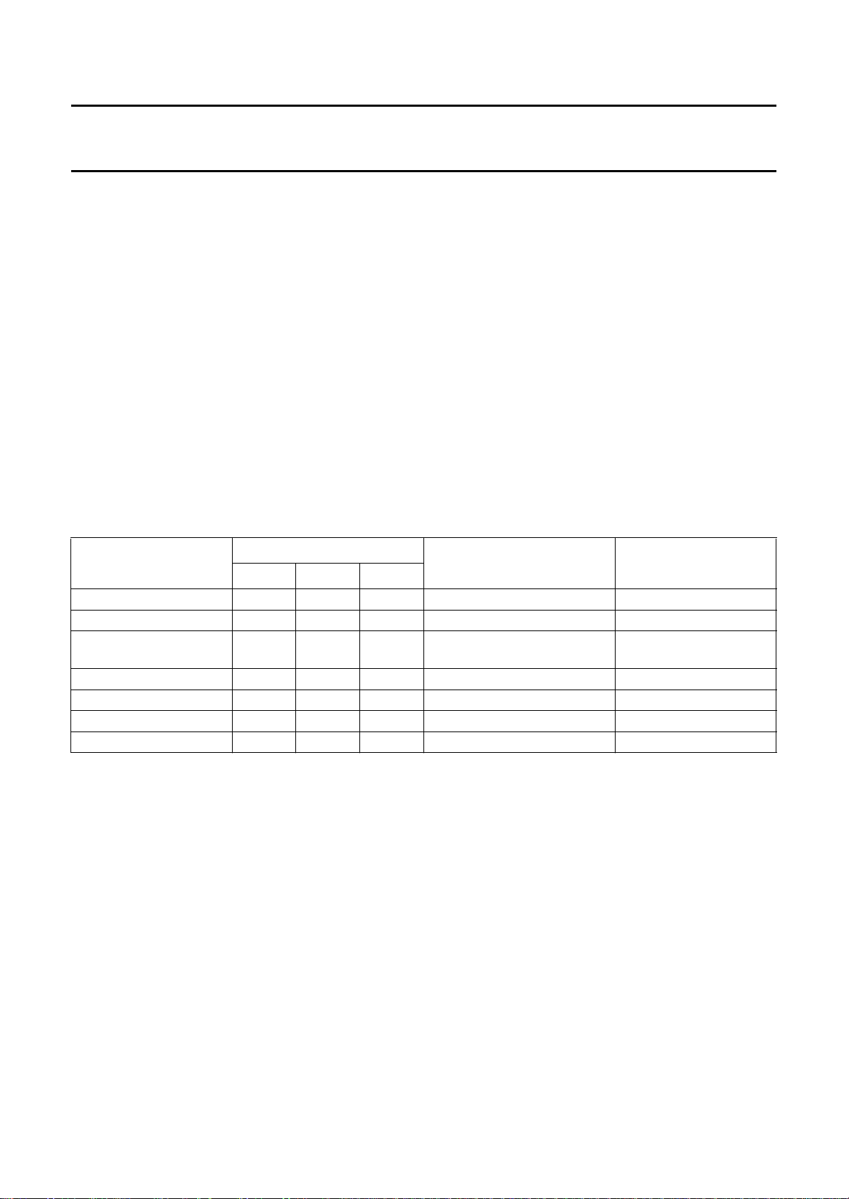
QUICK REFERENCE DATA
SYMBOL PARAMETER
CONDITIONS ON PINS
CS SA AB
V
DD
V
CCM
I
DDDCC+ICCM
I
DDACC+ICCM
I
DDRS
supply voltage −−−2.7 3.0 5.5 V
supply voltage feedback amplifiers −−−2.7 3.0 5.5 V
supply current DCC mode 1 0 X 28 39 53 mA
supply current ACC mode 1 1 X 26 35 47 mA
supply current reference sense
0 0 X 0.6 1.2 1.6 mA
current mode
I
DDAB
I
DDstb+ICCM
P
(tot)DCC
supply current sense AB mode 0 1 1 1.5 2.7 3.7 mA
supply current standby mode 0 1 0 − 0.2 0.3 mA
total power dissipation DCC mode;
10X−120 − mW
note 2
P
(tot)ACC
total power dissipation ACC mode;
11X−105 − mW
note 2
T
amb
operating ambient temperature −−−−30 − +85 °C
Notes
1. In the conditions column 0 = LOW; 1 = HIGH; X = don’t care.
2. V
DD=VCCM
= 3 V; I
DSEN
= 0; IFB=0.
(1)
MIN. TYP. MAX. UNIT
September 1994 3
Philips Semiconductors Preliminary specification
DCC read amplifier (READ 3) TDA1380
BLOCK DIAGRAM
September 1994 4
Fig.1 Block diagram.
Philips Semiconductors Preliminary specification
DCC read amplifier (READ 3) TDA1380
PINNING
SYMBOL PIN DESCRIPTION
DSENADJ1 1 adjustment pin for sense current 1
(A and B)
DSENADJ2 2 adjustment pin for sense current 2
(A and B)
DSENADJ3 3 adjustment pin for sense current 3
(A and B)
V
refSENA
V
refSENB
4 reference voltage output sense (A)
5 reference voltage output sense (B)
DSEN1B 6 sense current output 1 (B)
DSEN2B 7 sense current output 2 (B)
DSEN3B 8 sense current output 3 (B)
DSEN3A 9 sense current output 3 (A)
DSEN2A 10 sense current output 2 (A)
DSEN1A 11 sense current output 1 (A)
INX0B 12 auxiliary channel input/channel 0
input (B)
IN01B 13 channel 0 and 1 input (B)
IN1B 14 channel 1 input (B)
INX25B 15 channels AUX, 2 and 5 input (B)
IN23B 16 channels 2 and 3 input (B)
IN34B 17 channels 3 and 4 input (B)
IN4B 18 channel 4 input (B)
IN56B 19 channels 5 and 6 input (B)
IN67B 20 channels 6 and 7 input (B)
IN7B 21 channel 7 input (B)
IN7A 22 channel 7 input (A)
IN67A 23 channels 6 and 7 input (A)
IN56A 24 channels 5 and 6 input (A)
IN4A 25 channel 4 input (A)
IN34A 26 channels 3 and 4 input (A)
IN23A 27 channels 2 and 3 input (A)
INX25A 28 channels AUX, 2 and 5 input (A)
IN1A 29 channel 1 input (A)
IN01A 30 channels 0 and 1 input (A)
INX0A 31 auxiliary channel input/channel 0
input (A)
V10 32 reference voltage for DCC inputs
MFR2B 33 right channel feedback amplifier
output 2 (B)
MFR1AB 34 right channel feedback amplifier
output 1 (A and B)
SYMBOL PIN DESCRIPTION
MFR2A 35 right channel feedback amplifier
output 2 (A)
INMFR 36 right channel feedback amplifier
input
OUTRA 37 right channel ACC output (A)
OUTRB 38 right channel ACC output (B)
INEQR 39 right channel equalization amplifier
input
OUTEQR 40 right channel equalization amplifier
output
V
CCM
41 supply voltage for feedback
amplifiers
V
EEM
42 ground for feedback amplifiers
OUTEQL 43 left channel equalization amplifier
output
INEQL 44 left channel equalization amplifier
input
OUTLB 45 left channel ACC output (B)
OUTLA 46 left channel ACC output (A)
INMFL 47 left channel feedback amplifier input
MFL2A 48 left channel feedback amplifier
output 2 (A)
MFL1AB 49 left channel feedback amplifier
output 1 (A and B)
MFL2B 50 left channel feedback amplifier
output 2 (B)
V
ref
V
refADC
51 reference voltage output
52 ADC reference voltage output
AB 53 tape sector A or B selection input
RDSYNC 54 read sync pulse input
RDCLK 55 read clock pulse input
SA 56 select ACC mode input
V
SS
V
DD
57 ground
58 supply voltage
CS 59 chip select input
AGC 60 AGC time constant
VBIAS 61 preamplifier gain control voltage
input
RDMUX 62 output of sampled and multiplexed
auxiliary and main data signals
OUTX 63 auxiliary channel preamplifier output
MUXINX 64 auxiliary channel multiplexer input
September 1994 5
Philips Semiconductors Preliminary specification
DCC read amplifier (READ 3) TDA1380
September 1994 6
Fig.2 Pin configuration.

Philips Semiconductors Preliminary specification
DCC read amplifier (READ 3) TDA1380
FUNCTIONAL DESCRIPTION
DCC data amplifiers and filters
The TDA1380 has 18 low-noise preamplifiers, which are
connected to an 18-channel MRH. For each tape sector
the MRH is partitioned into three strings of three heads
(see Fig.11). Depending on the tape sector selection
signal AB, nine preamplifiers for the A-sector, or nine
preamplifiers for the B-sector of the tape are selected.
Eight of the nine channels are for the DCC main data, and
one for the auxiliary (AUX) data. The eight main data
channels have pre-equalization for frequencies from 1 kHz
up to 50 kHz (1st order highpass, −3 dB at 75 kHz), and
lowpass filtering for anti-aliasing (2nd order active, −3dB
at 120 kHz). The AUX channel has a flat frequency
response. The AUX data is continuously available at
output OUTX. This output must be AC-coupled to the
multiplexer input MUXINX. All inputs must be AC-coupled
to the MRH. The inputs are internally biased at pin V10.
The voltage at pin V10 is temperature dependent and is
not intended for external use. Pin V10 has to be decoupled
to the positive supply voltage (V
DD
).
Automatic gain control
The DCC part is equipped with an AGC circuit which
decreases the gain of the preamplifiers when the level at
RDMUX exceeds a preset value. In this way an optimum
voltage swing at the RDMUX output is obtained (for the
ADC input of SAA2051, SAA2032, SAA2023 or
SAA3323). The response time of the AGC can be set by
an external capacitor connected to pin 60. There is a fixed
relationship between the source and sink current at this
pin, resulting in a fixed relationship between the decay
time and the recover time of the preamplifier gain. The
AGC is active only in the DCC mode and can be switched
off by connecting pin 60 to V
SS
.
Multiplexer
A multiplexing circuit switches the nine digital channels
sequentially to the output. The AUX data is sampled during
two clock periods, the eight main data channels are
sampled during one clock period. The effective sample
frequency is one tenth of the clock frequency at RDCLK. A
timing overview is illustrated in Fig.4.
Analog amplifiers
For ACC playback the TDA1380 employs four DCC
preamplifiers (per tape sector) for amplification of the left
and right analog signals. Amplifiers CHX and CH0 are
used for the left channel and CH4 and CH5 for the right
channel. The buffered left and right channel outputs are
available at four pins (see Table 1). Pins that carry no left
and right channel signals will have a DC level V
.
A
Table 1 ACC playback.
AB
1 A left V
0BV
TAPE
SELECT
OUTLA OUTLB OUTRA OUTRB REMARKS
A
A
right V
left V
A
A
right
allows separate amplitude
adjustment for sectors A and B
1 A left note 1 right note 1 allows one amplitude setting
0 B left note 1 right note 1
only for sectors A and B
(DSP operation; high feedback
operation)
Note
1. At least one of OUTLB and OUTRB are externally connected to VDD.
September 1994 7
Philips Semiconductors Preliminary specification
DCC read amplifier (READ 3) TDA1380
Feedback amplifiers
Two feedback amplifiers are available for driving a
conductor in the MRH, thus providing magnetic feedback
to improve the linearity of the analog audio response. In
both the ACC and DCC mode, the feedback amplifiers are
used for DC biasing of the MRH. The circuit principle of the
feedback amplifiers is illustrated in Fig.9.
Current and voltage sources
Separate, adjustable low-noise current sources are
available to provide the sense currents to the MRHs. The
active current outputs are controlled by the mode switch
(see Table 2). In the reference sense current mode, only
one source is active (DSEN1B, pin 6). This current can be
used for temperature measurement of the DCC head,
thereby enabling control of the write current (TDA1381)
Equalization amplifiers
Two uncommitted operational amplifiers are available for
pre-equalization of the left and right ACC outputs. These
amplifiers are only operational during ACC playback. The
non-inverting input is internally connected to a DC voltage
which is approximately equal to V
If the amplifiers are
ref.
not used in the application, it is advised to connect the
outputs to the inputs.
when recording. The principle of the sense current sources
is illustrated in Fig.8. The typical value of the output current
is determined by resistors connected between the adjust
pins and V
; where I
SS
The DC output voltages V
V
are derived from an internal bandgap reference
refSENB
voltage source. The voltage V
DSEN
= 0.33/R
, V
ADC
refADC
.
ADJUST
, V10, V
ref
refSENA
(referenced to VSS)
and
can be used as a reference voltage for analog-to-digital
conversion of the RDMUX output.
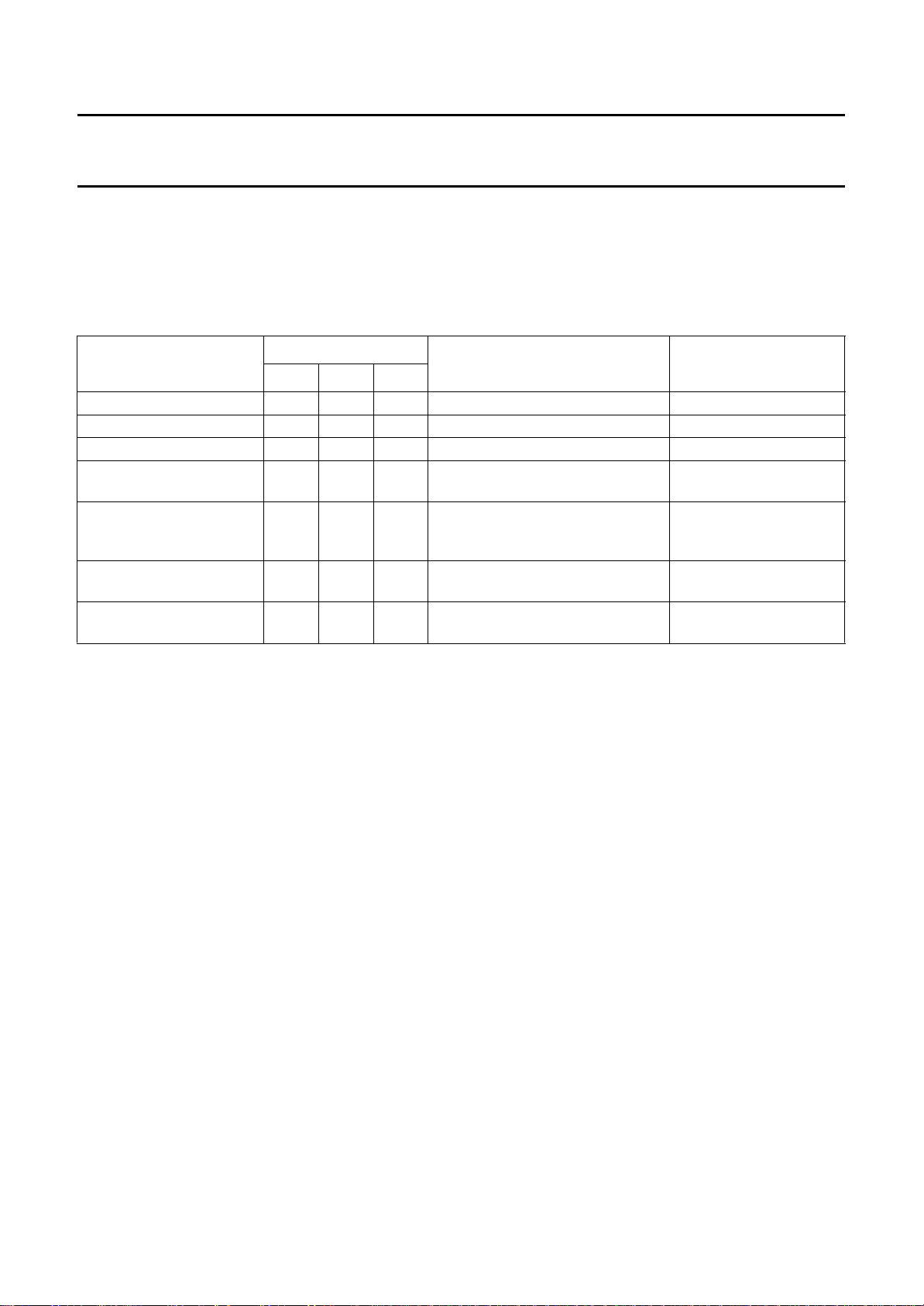
Table 2 Sense current sources.
MODE
DIGITAL INPUTS
CS SA AB
(1)
AVAILABLE SENSE
CURRENT
ACTIVE DC OUTPUTS
Standby 0 1 0 −−
Reference sense current 0 0 X DSEN1B −
Sense AB 0 1 1 DSEN1A; DSEN2A; DSEN3A
DSEN1B; DSEN2B; DSEN3B
ACC playback A 1 1 1 DSEN1A; DSEN2A; DSEN3A V
ACC playback B 1 1 0 DSEN1B; DSEN2B; DSEN3B V
DCC playback A 1 0 1 DSEN1A; DSEN2A; DSEN3A V
DCC playback B 1 0 0 DSEN1B; DSEN2B; DSEN3B V
V
refSENA
V
refSENB
refSENA
refSENB
refSENA
refSENB
Note
1. Where X = don't care; 0 = LOW; 1 = HIGH.
September 1994 8
Philips Semiconductors Preliminary specification
DCC read amplifier (READ 3) TDA1380
Modes of operation
The amplifiers and sense current sources for the ACC and DCC parts can be switched ON/OFF separately by the mode
switch signals CS, SA and AB. Also, a connection between OUTLB or OUTRB or both to VDD is recognized as a single
output ACC mode where the left and right outputs are present at OUTLA and OUTRA only.
Table 3 Modes of operation.
MODE
DIGITAL INPUT
CS SA AB
Standby 0 1 0
Reference sense current 0 0 X reference sense current source V
Sense AB 0 1 1 sense current sources V
ACC playback A/B 1 1 1 or 0 sense currents, data preamplifiers,
ACC playback A/B via
1 1 1 or 0 sense currents, data preamplifiers,
OUTLA and OUTRA only
(note 2)
DCC playback A/B 1 0 1 or 0 sense currents, data amplifiers and
Test mode (note 3) 1 0 1 or 0 sense currents, data amplifiers and
(1)
ACTIVE PARTS
(see Fig.1)
AN, EQ and FB
AN, EQ and FB
filters, multiplexer, AGC and FB
filters, multiplexer, AGC and FB
ACTIVE DC
REFERENCE OUTPUTS
ref
ref
V
; V10
ref
V
; V10
ref
; V10; V
V
ref
V
ref
; V10; V
refADC
refADC
Notes
1. Where X = don't care; 0 = LOW; 1 = HIGH.
2. At least one of OUTLB or OUTRB are externally connected to V
3. INEQL or INEQR connected to VDD (no user function).
DD
.
September 1994 9
 Loading...