

Philips TDA1373H Datasheet
INTEGRATED CIRCUITS
DATA SH EET
TDA1373H
General Digital Input (GDIN)
Product specification
Supersedes data of 1995 Aug 28
File under Integrated Circuits, IC01
1996 Jul 17

Philips Semiconductors Product specification
General Digital Input (GDIN) TDA1373H
FEATURES
• Four operating modes:
– Sample Rate Conversion (SRC) mode
– AD/DA mode
– SLAVE-VCO mode
– SLAVE-VCXO mode
• Full digital sample rate conversion over a wide range of
input sample rates
• Fast and automatic detection and locking to the input
sample rate with continuous tracking
• Digital Phase-Locked Loop (PLL) with adaptive
bandwidth which removes jitter on the digital audio input
• Audio outputs (soft) muted during loop acquisition
• Full linear phase processing based on all-FIR filtering
• Integrated full digital IEC 958 demodulator for digital
input signals (AES/EBU or SPDIF format) with intelligent
error handling
• Extended input sample frequency range
• IEC 958 Channel Status (CS) and User Channel (UC)
outputs
• On-chip CS and/or UC demodulation and buffering
(consumer and professional format)
• Dedicated subcode processing for Compact Disc (CD)
• Final output quantization to 16, 18 or 20 bits with
optional in-audio-band noise shaping
• Bitstream input and output for coupling with 1-bit
analog-to-digital conversion (ADC) and digital-to-analog
conversion (DAC)
2
S and Japanese serial input formats supported for
• I
SRC and DAC functions
• I2S and Japanese serial output formats supported for
SRC and ADC functions
• I2S and Japanese 4× oversampled serial output
available for SRC and ADC functions
• 8-bit digital gain/attenuation control
• Switchable Digital Signal Processor (DSP)-interface
(I2S input and output) for additional audio processing
• Additional clock outputs available at 768, 384, 256 and
128f
so
• 3-line serial microcontroller interface, compatible with
the Philips CD I.C. protocol (HCL)
• 5 V power supply
• 0.7 µm double metal Complementary Metal Oxide
Semiconductor (CMOS)
• SRC THD + N:
– −113 dB over the 0 to 20 kHz band (1 kHz, 20 bits
input and output) (see Fig.3)
– −95 dB over the 0 to 20 kHz band (1 kHz, 16 bits
input and output)
• Pass band ripple smaller than ±0.004 dB for
up-sampling and down-sampling filters
• Stop band suppression:
– selectable between 70 dB and 50 dB for 64×
up-sampling filters
– 80 dB for 128× down-sampling filters
• Microcontroller operated and stand-alone mode.
APPLICATIONS
• Professional audio equipment for:
– mixing
– recording
– editing
– broadcasting
• CD-Recordable (CD-R)
• Digital Speaker Systems (DSS)
• Digital Compact Cassette recorders (DCC)
• Digital Audio Tape (DAT) and MD recorders
• Digital amplifiers
• Jitter killers.
1996 Jul 17 2

Philips Semiconductors Product specification
General Digital Input (GDIN) TDA1373H
GENERAL DESCRIPTION
The TDA1373H is a General Digital Input (GDIN) device
for audio signals which is able to perform a high-quality
sample rate conversion of digital audio signals (SRC
mode). The device reads several serial input formats and
signals in the IEC 958 digital audio format (also known as
AES/EBU or SPDIF signals). For this purpose a full Audio
Digital Input Circuit (ADIC) is present in the device.
An internal digital PLL results in extensive jitter removal
from incoming digital audio signals without any analog
loop electronics. The standard 20 bit output word length
The GDIN digital filters can also be reused for Bitstream
ADC and DAC conversion (AD/DA mode). The internal
digital PLL can be reconfigured to operate the GDIN in a
slave mode, where the output sample frequency of the
device is locked to the incoming sample rate
(SLAVE-VCO and SLAVE-VCXO modes).
The combination of an ADIC function, sample rate
conversion and Bitstream ADC and DAC results in a
device with a highly versatile functionality and large
replacement value in consumer and professional
audio sets.
can be limited to 16 or 18 bits by means of ‘in-audio-band
noise shaping’.
QUICK REFERENCE DATA
All inputs and outputs CMOS compatible; unless otherwise specified.
SYMBOL PARAMETER CONDITIONS MIN. TYP. MAX. UNIT
Supply
V
DD
I
DD(tot)
P
tot
supply voltage fso> 44.1 kHz 4.75 5 5.5 V
≤ 44.1 kHz 4.5 5 5.5 V
f
so
total supply current fso= 44.1 kHz − 155 − mA
total power dissipation fso= 44.1 kHz − 775 − mW
= 49 kHz;
f
so
− 1030 − mW
VDD= 5.5 V
IEC 958 input DI1S (high-sensitivity IEC input)
V
i(p-p)
AC input voltage
0.2 − V
(peak-to-peak value)
Clock and timing
f
so(max)
maximum output sample frequency VDD= 4.75 V 49 55 − kHz
Temperature
T
amb
operating ambient temperature 0 70 °C
ORDERING INFORMATION
TYPE
NUMBER
NAME DESCRIPTION VERSION
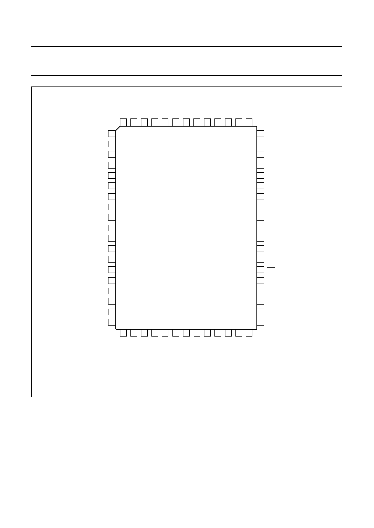
PACKAGE
TDA1373H QFP64 Plastic quad flat package; 64 leads (lead length 1.95 mm);
body 14 × 20 × 2.7 mm; high stand-off height
DD
SOT319-1
V
1996 Jul 17 3
Philips Semiconductors Product specification
General Digital Input (GDIN) TDA1373H
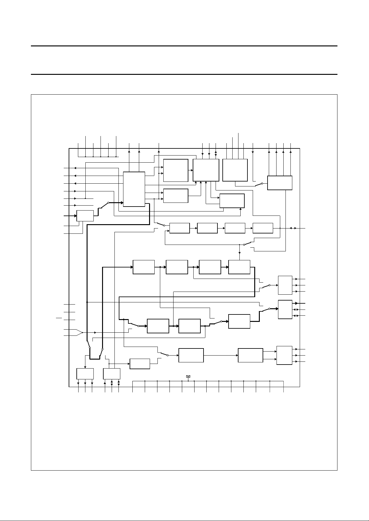
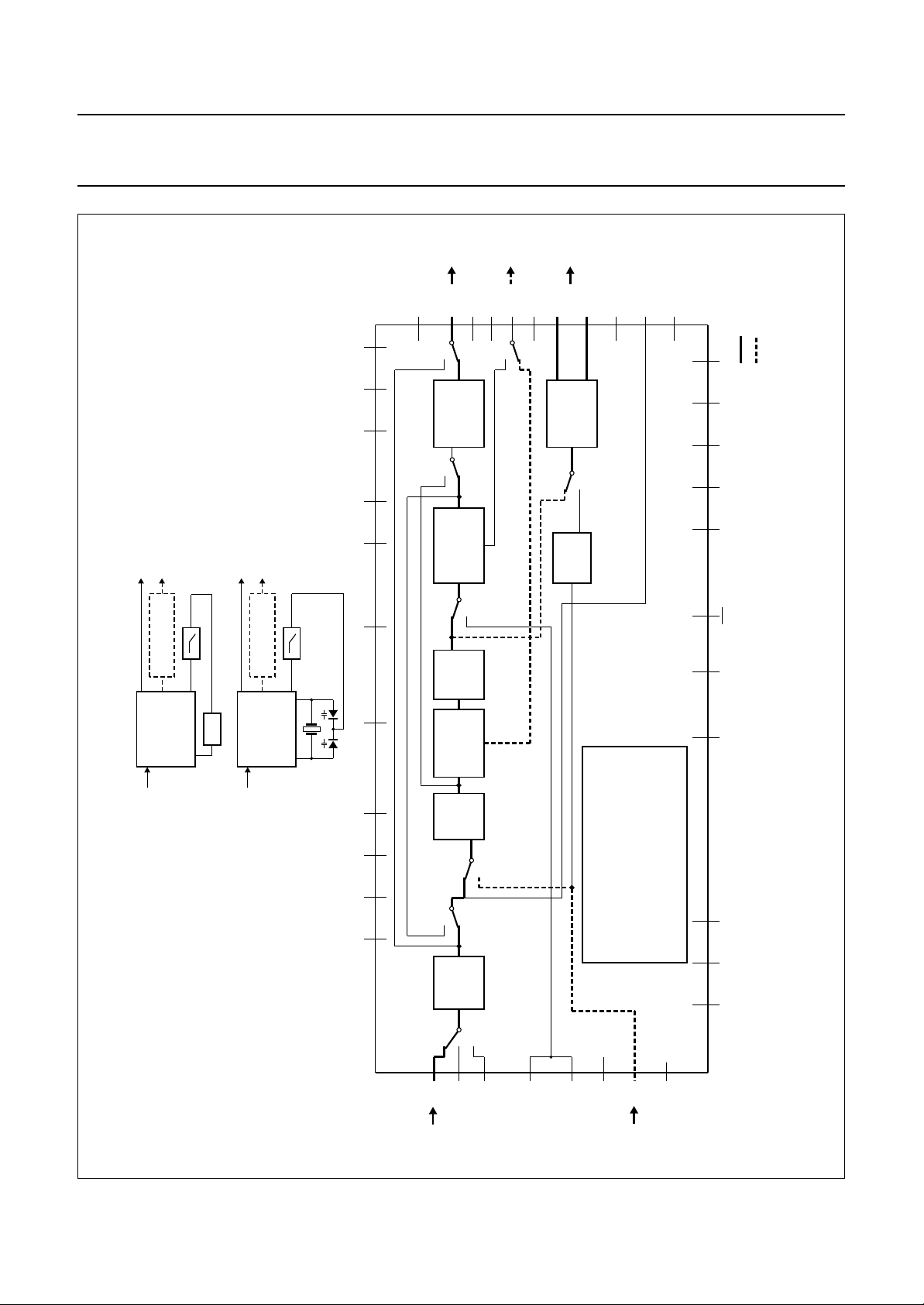
BLOCK DIAGRAM
V
SSA4
V
DDA4
CRYSTAL
OSCILLATOR
GENERAL
CONTROL
HOLD VCO
MM0
23 27 28 30 312221 19 204645473536345239 14327
MM1
CLO4CLO3CLO2CLO1CLIXTLOXTLIDA
so
768fso384fso256fso128f
CLOCK
SHOP
64f
so
25
FSL
handbook, full pagewidth
MU
EM
LOCK
SA
DI1D
DI1O
DI1S
V
DDA1
V
SSA1
DDDVDDDVDDD
V
DDD
DDDVDDD
11
44
37
48
43
62
63
1
DATA
SLICER
3
2
V
V
USER
CHANNEL
EXTRACTION
CHANNEL
EXTRACTION
DI2
STATUS
PHASE
DETECTOR
DI1
ADIC
(IEC 958
DECODER)
U
PV
C
WS
PO
LDCLCENCUSBS
MICRO-
CONTROLLER
INTERFACE/
STAND-ALONE
CONTROL
LOOP
FILTER
TST1
TST2
RST
AIL
AIR
42
41
38
4
5
stereo
FOD
FOS
2
I S OUT
55
FOC
FIFO
AND
GAIN
DNI
DI2
HOLD
2
I S IN
8
60
59
57
54
56
V
DI2C
DI2W
DI2D
FOW
SSD
V
12
SSD
32 x
DOWN-
SAMPLING
V
SSD
4 x
UP-
SAMPLING
SAMPLING
AOS
13 24
V
SSD
17
V
SSD
ATTENUATOR
4 x
DOWN-
16 x
UP-
SAMPLING
INS
VARIABLE
HOLD
IN-BAND
NOISE
SHAPER
BITSTREAM
DIGITAL
FILTER
DO2
DSO
2
I S
OUT
2
I S
OUT
DAC
OUTPUT
10
DO2D
16
DO2W
6
DO2C
50
DO1D
49
DO1W
51
DO1C
9
AOL1
15
AOR1
18
CLD
TDA1373H
33
40
26
29
V
V
SSD
V
SSD
SSD
53
58
61
64
V
SSD
V
V
SSD
SSD
SSDVSSD
MLC334 - 2
V
Switches MM1 and MM0 are controlled indirectly via the mode selection. All other switches can be controlled directly by the user.
Fig.1 Block diagram.
1996 Jul 17 4
Philips Semiconductors Product specification
General Digital Input (GDIN) TDA1373H
PINNING
SYMBOL PIN DESCRIPTION TYPE
DI1S 1 IEC 958 digital audio input ‘S’ (200 mV peak-to-peak value) E036A
V
SSA1
V
DDA1
AIL 4 Bitstream audio input left HPP01
AIR 5 Bitstream audio input right HPP01
DO2C 6 serial digital audio output 2; bit clock output (192f
V
DDD
V
SSD
AOL1 9 Bitstream audio output left OPF40
DO2D 10 DLO = 0; serial digital audio output 2; data;
V
DDD
V
SSD
V
SSD
V
DDD
AOR1 15 Bitstream audio output right OPF40
DO2W 16 DLO = 0; serial digital audio output 2; word select output (4f
V
SSD
CLD 18 Bitstream DAC clock (192 or 128f
V
DDA4
V
SSA4
XTLI 21 crystal input 768f
XTLO 22 crystal output OSX01
CLI 23 external VCO input (SLAVE-VCO mode only) HPP01
V
SSD
FSL 25 SA = 0 (microcontroller operated) external VCO output (slave modes
V
SSD
CLO1 27 clock output 768f
CLO2 28 clock output 384f
V
SSD
CLO3 30 clock output 256f
CLO4 31 clock output 128f
V
DDD
V
SSD
BS 34 block sync; channel status/user channel/CD subcode OPF40
CEN 35 data enable; channel status/user channel/CD subcode OPF40
CUS 36 data bit; channel status/user channel/CD subcode OPF40
EM 37 IEC 958 source pre-emphasis flag OPF20
2 IEC 958 slicer analog ground E038A
3 IEC 958 slicer analog supply voltage E037A
) OPF40
so
7 digital supply voltage; note 1 −
8 digital ground; note 2 −
OPF40
DLO = 1; Bitstream audio output left inverted (
AOL1); note 3
11 digital supply voltage; note 1 −
12 digital ground; note 2 −
13 digital ground; note 2 −
14 digital supply voltage; note 1 −
);
so
OPF40
DLO = 1; Bitstream audio output right inverted (AOR1); note 3
17 digital ground; note 2 −
) OPF43
so
19 oscillator analog supply voltage E037A
20 oscillator analog ground E038A
so
OSX01
24 digital ground; note 2 −
HOF21
only); SA = 1 (stand-alone control) DI11 control line; note 4
26 digital ground; note 2 −
so
so
OPF40
OPF40
29 digital ground; note 2 −
so
; OPF40
so
OPF40
32 digital supply voltage; note 1 −
33 digital ground; note 2 −
1996 Jul 17 5
Philips Semiconductors Product specification
General Digital Input (GDIN) TDA1373H
SYMBOL PIN DESCRIPTION TYPE
RST 38 power-on reset input (active LOW) HPP07
V
DDD
V
SSD
TST2 41 test pin 2 (LOW for normal operation) HPP01
TST1 42 test pin 1 (LOW for normal operation) HPP01
SA 43 Stand-alone/microcontroller operated selection;
MU 44 mute flag (active HIGH) OPF40
LD 45 SA = 0 (microcontroller operated) microcontroller interface; load
DA 46 SA = 0 (microcontroller operated) microcontroller interface (data);
CL 47 SA = 0 (microcontroller operated) microcontroller interface (clock);
LOCK 48 ADIC lock flag (active HIGH) OPF40
DO1W 49 serial digital audio output 1; word select input/output (f
DO1D 50 serial digital audio output 1; data OPF43
DO1C 51 serial digital audio output 1; bit clock input/output (48f
V
DDD
V
SSD
FOW 54 serial digital audio feature output; word select OPF43
FOD 55 serial digital audio feature output; data OPF43
FOC 56 serial digital audio feature output; bit clock (64f
DI2D 57 serial digital audio input 2; data HPP01
V
SSD
DI2W 59 serial digital audio input 2; word select HOF21
DI2C 60 serial digital audio input 2; bit clock output HOF21
V
SSD
DI1D 62 SA = 0 (microcontroller operated) IEC 958 digital audio input ‘D’ (CMOS
DI1O 63 IEC 958 digital audio input ‘O’ (CMOS level) HPP01
V
SSD
Notes
1. All V
2. All V
pins are internally connected.
DDD
pins are internally connected.
SSD
3. DLO is a command flag from register 4 (see Section “Command registers”).
4. SA is the stand-alone/microcontroller operated pin (pin 43). DI11, NSD, DI2, QU1, QU0 and MS0 are command flags
to control the operation of the device. For more information see Section “Controlling the GDIN”.
39 digital supply voltage; note 1 −
40 digital ground; note 2 −
HPP01
SA = 1 for stand-alone operation
HPP01
(read/write); SA = 1 (stand-alone control) NSD control line; note 4
HOF41
SA = 1 (stand-alone control) DI2 control line; note 4
HPP01
SA = 1 (stand-alone control) QU1/QU0 control line; note 4
) HOF41
so
) HOF41
so
52 digital supply voltage; note 1 −
53 digital ground; note 2 −
) OPF43
so
58 digital ground; note 2 −
61 digital ground; note 2 −
HPP01
level); SA = 1 (stand-alone control) MSO control line; note 4
64 digital ground; note 2 −
1996 Jul 17 6
Philips Semiconductors Product specification
General Digital Input (GDIN) TDA1373H
handbook, full pagewidth
DI1S
V
SSA1
V
DDA1
DO2C
V
DDD
V
SSD
AOL1
DO2D
V
DDD
V
SSD
V
SSD
V
DDD
AOR1
DO2W
V
SSD
CLD
V
DDA4
AIL
AIR
SSD
V
DI1O
64
63
1
2
3
4
5
6
7
8
9
10
11
12
13
14
15
16
17
18
19
DI1D
62
SSD
V
61
DI2C
60
SSD
V
DI2W
59
58
TDA1373H
DI2D
57
FOC
56
FOD
55
FOW
54
SSD
V
53
DDD
V
52
51
DO1C
DO1D
50
49
DO1W
48
LOCK
CL
47
DA
46
45
LD
44
MU
SA
43
TST1
42
TST2
41
V
40
SSD
V
39
DDD
38
RST
EM
37
CUS
36
35
CEN
BS
34
V
33
SSD
20
21
SSA4
V
XTLI
22
XTLO
23
CLI
24
SSD
V
25
FSL
Fig.2 Pin configuration.
1996 Jul 17 7
26
V
SSD
27
CLO1
28
CLO2
29
SSD
V
30
CLO3
31
CLO4
32
DDD
V
MLB955 - 2

Philips Semiconductors Product specification
General Digital Input (GDIN) TDA1373H
FUNCTIONAL DESCRIPTION
Operating modes
AMPLE RATE CONVERSION (SRC) MODE
S
The output sample rate is determined by a crystal and can
be chosen up to 49 kHz. The range of input sample rates
for a given output sample rate is given in Table 1. A pitch
variation (‘Varispeed’) of ±12% around the nominal input
sample rate can be tracked.
Table 1 Input sample rates
OUTPUT SAMPLE RATE
(kHz)
2
I
S INPUT (kHz)
0.3 to 1.7f
48 13 to 83 16 to 68
44.1 12 to 76 15 to 62
32 9to55 12to45
60
handbook, full pagewidth
THD N
(dB)
80
Data path
(see Fig.4)
The input signal at sample frequency fsi comes in via one
of the DI1 inputs (IEC 958) or via the serial input DI2X.
The signal passes through the FIFO/GAIN part and is
interpolated in the up-sampling filters. The actual sample
rate conversion takes place in the variable hold block. The
down-sampling filters decimate the sample frequency to
fso and after in-band noise shaping, the output signal is
present at serial output DO1. Additionally the converted
signal is available at the ‘analog’ Bitstream outputs AOL,
AOR and at the serial digital output DO2 (4f
).
so
IEC 958 INPUT (kHz)
so
0.35 to 1.45f
so
MLB956
100
120
140
160
10
Measurement done with ‘Audio Precision’.
SRC mode; 48 to 44.1 kHz; 20-bit output.
2
10
Fig.3 Total harmonic distortion plus noise as a function of frequency.
1996 Jul 17 8
3
10
4
10
f (Hz)
5
10

Philips Semiconductors Product specification
General Digital Input (GDIN) TDA1373H
DO1C
DO1D
DO1W
DO2C
DO2D
DO2W
AOL
AOR
FOC
FOD
FOW
MLC335
Main path.
Example of
additional path.
TST2TST1CLIXTLIXTLOLOCKEMCUSCENBSFSL
DSO
DO2
CLD
2
digital output
digital input
analog output
fsoI S
DAC
BITSTREAM
TDA1373H
2
fsiAES/EBU or I S
e.g. TDA1547
so
768f
NOISE
IN-BAND
SHAPER
INS
DOWN-
SAMPLING
32 x AND 4 x
DNI
HOLD
VARIABLE
4 x AND 16 x
UP-SAMPLING
&
FIFO
GAIN
AOS
TDA1373H
FILTER
DIGITAL
BITSTREAM
HOLD
CS AND UC
DIGITAL PLL
EXTRACTION
CLO4CLO3CLO2CLO1RSTSAMUDALDCL
handbook, full pagewidth
Fig.4 Standard data path in the SRC mode.
DI2
FOS
ADIC
(IEC 958
DECODER)
DI1
DI1S
DI1O
DI1D
AIL
1996 Jul 17 9
AIR
INTERFACE
CLOCK SHOP
MICROCONTROLLER
DI2C
DI2D
GENERAL CONTROL
DI2W

Philips Semiconductors Product specification
General Digital Input (GDIN) TDA1373H
SLAVE-VCO AND SLAVE-VCXO MODES
In the SLAVE-VCO and SLAVE-VCXO modes, the GDIN
can pass an exact copy of the incoming samples to the
output, e.g. for storage on a digital medium such as CD-R.
The output sample rate tracks any input sample rate within
the frequency range of the external VC(X)O (fso=fsi).
In the SLAVE-VCO mode a pitch variation of ±12.5%
around the nominal sample frequency can be tolerated.
Data path
The signal at input sample frequency fsi comes in via one
of the DI1 inputs (IEC 958).
The ADIC signal passes through the FIFO/GAIN block and
can be fed through the IN-BAND NOISE SHAPER to the
serial output DO1. Additionally, the signal is present at
DO2 (4fso) and at the Bitstream outputs AOL and AOR.
Exact copies for digital use (e.g. write to a disk) from the
input signal can be retrieved at output FO (this signal might
be affected by jitter since it has not passed through the
FIFO/GAIN block). By means of data path switch DSO, this
direct output of the ADIC block can also be fed to
output DO1. Note that in this event the DO1 serial format
becomes equal to the FO format (see Table 3).
(see Fig.5)
AD/DA
In this mode, the GDIN supports an economic realization
of analog-to-digital and digital-to-analog conversion, in
accordance with the Bitstream principle. This requires a
Bitstream sigma-delta modulator and a Bitstream DAC,
since the up-sampling and down-sampling filters of the
sample rate convertor are reused. ADC and DAC can be
simultaneously performed.
Data path DA conversion
The signal at sample frequency fso comes in via serial input
DI2X or via one of the DI1 inputs (IEC 958). The signal
passes through the FIFO/GAIN part and is interpolated in
the up-sampling filters. A Bitstream digital filter converts
this signal into a Bitstream signal at outputs AOL and AOR,
after which it can be filtered by a Bitstream DAC like the
TDA1547.
Data path AD conversion
The Bitstream signal from the sigma-delta modulator
enters the GDIN at inputs AIL and AIR. The
down-sampling filters decimate this signal to fso and after
in-band noise shaping (selectable), the output signal is
present at serial output DO1.
MODE
(see Fig.6)
(see Fig.6)
1996 Jul 17 10
Philips Semiconductors Product specification
General Digital Input (GDIN) TDA1373H
DO1C
DO1D
DO1W
DO2C
DO2D
DO2W
AOL
AOR
FOC
FOD
FOW
MLC336
Main path.
Example of
additional path.
TST2TST1CLIXTLIXTLOLOCKEMCUSCENBSFSL
DSO
DO2
CLD
2
digital output
analog output
fsiI S
BITSTREAM
TDA1373H
2
digital input
fsiAES/EBU or I S
digital output
fsiI S
DAC e.g.TDA1547
VCO
digital input
2
analog output
BITSTREAM
DAC e.g.TDA1547
TDA1373H
2
fsiAES/EBU or I S
so
768f
NOISE
IN-BAND
SHAPER
INS
DOWN-
SAMPLING
32 x AND 4 x
DNI
HOLD
VARIABLE
4 x AND 16 x
UP-SAMPLING
&
FIFO
GAIN
DI2
TDA1373H
FILTER
DIGITAL
BITSTREAM
AOS
HOLD
CS AND UC
DIGITAL PLL
CLO4CLO3CLO2CLO1RSTSAMUDALDCL
handbook, full pagewidth
EXTRACTION
FOS
ADIC
DI1
DI1S
1996 Jul 17 11
(IEC 958
DECODER)
DI1O
DI1D
AIL
AIR
INTERFACE
CLOCK SHOP
MICROCONTROLLER
DI2C
DI2D
GENERAL CONTROL
Fig.5 Standard data path in the SLAVE-VCO and SLAVE-VCXO modes.
DI2W

Philips Semiconductors Product specification
General Digital Input (GDIN) TDA1373H
2
digital output
fsoI S
TDA1373H
analog output
DAC
BITSTREAM
e.g. TDA1547
so
768f
TST2TST1CLIXTLIXTLOLOCKEMCUSCENBSFSL
DO1C
AD OUT
DO1D
DSO
NOISE
IN-BAND
SHAPER
INS
DOWN-
SAMPLING
32 x AND 4 x
DNI
HOLD
VARIABLE
DO1W
DO2C
DO2D
DO2
DO2W
DA OUT
AOL
AOR
FILTER
DIGITAL
BITSTREAM
AOS
HOLD
FOC
FOD
FOW
MLC337
Main path.
CLD
CLO4CLO3CLO2CLO1RSTSAMUDALDCL
Example of
additional path.
handbook, full pagewidth
4 x AND 16 x
UP-SAMPLING
ADC
BITSTREAM
e.g. SAA7360
digital input
analog input
2
fsoAES/EBU or I S
DI1S
DA IN
FOS
FIFO
ADIC
DI1
&
GAIN
DI2
(IEC 958
DECODER)
DI1O
DI1D
1996 Jul 17 12
TDA1373H
AIL
AD IN
AIR
CS AND UC
DIGITAL PLL
INTERFACE
CLOCK SHOP
MICROCONTROLLER
DI2C
DI2D
EXTRACTION
Fig.6 Standard data paths in the AD/DA mode.
GENERAL CONTROL
DI2W
 Loading...