

INTEGRATED CIRCUITS
DATA SH EET
TDA1318
DCC read amplifier
Preliminary specification
File under Integrated Circuits, IC01
Philips Semiconductors
April 1996

Philips Semiconductors Preliminary specification
DCC read amplifier TDA1318
FEATURES
• Differential inputs for a low-power head configuration
• Low-noise current sources for the sense currents of the
DCC head
• Reduced power consumption by separate on/off
switching of the circuits and sense current of the DCC
and CC parts of the IC
• The IC can be used with both the first and second
generation DCC digital signal processing ICs
• High-impedance outputs in the OFF state so that the
outputs of the ICs can be connected in parallel for dual
decks or for decks with electrical auto-reverse heads
• AGC of DCC preamplifiers (can be switched off)
• Possibility of analog audio via DCC preamplifiers
(analog via digital readers, ADR mode)
• Single 5 V supply.
GENERAL DESCRIPTION
The TDA1318 amplifies, filters and multiplexes signals
arriving from magneto-resistive thin film heads (MRHs)
which are suitable for DCC (Digital Compact Cassette)
and CC (Compact Cassette) systems. The device also has
current sources to provide sense currents through the
DCC-MRHs and two amplifiers for magnetic feedback and
biasing.
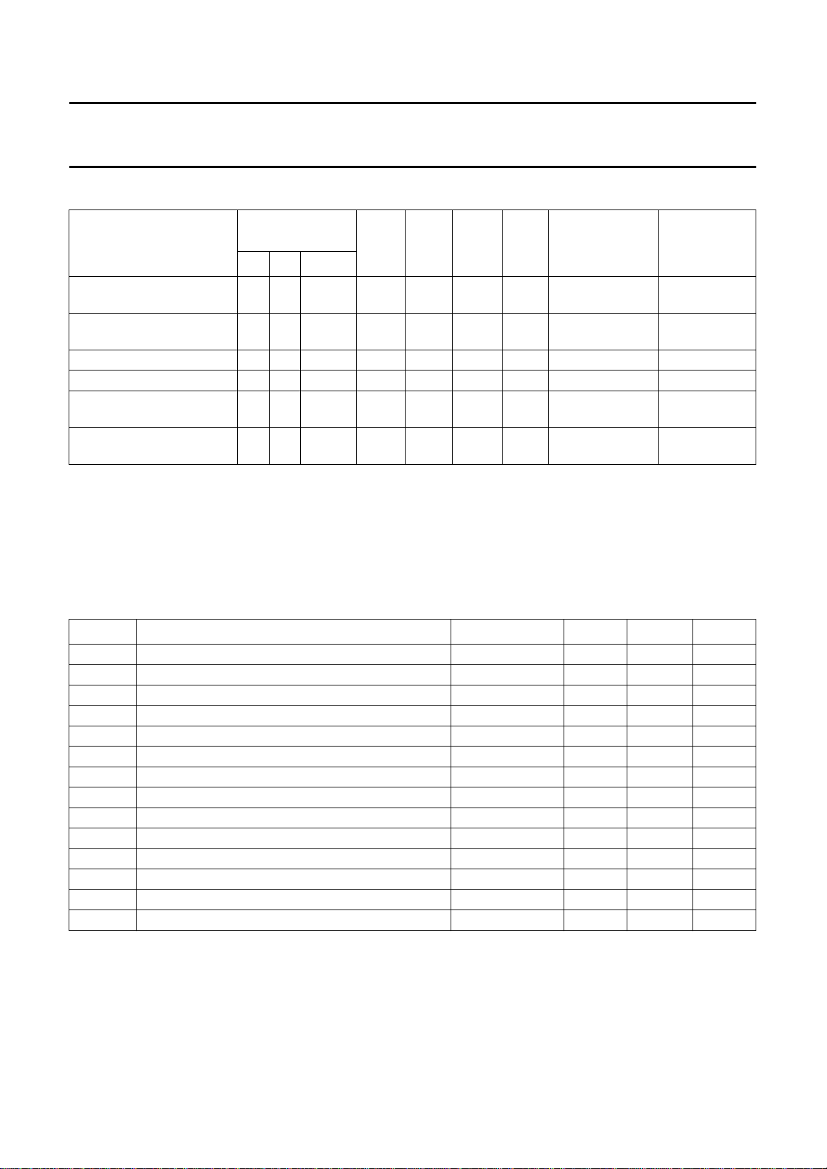
QUICK REFERENCE DATA
SYMBOL PARAMETER
V
DD
V
CCM
I
DDDCC
I
DDDCCadr
I
DDCC
I
DDCCadr
I
CCM
I
DD
I
DD(Q)
P
tot
T
amb
supply voltage −− −4.5 5.0 5.5 V
supply voltage feedback amplifiers −− −4.5 5.0 5.5 V
supply current DCC mode (note 2) 1 1 0 − 31 41 mA
supply current DCC mode (ADR) 1 1 1 − 31 41 mA
supply current CC mode 1 0 0 − 9.7 13 mA
supply current CC mode (ADR) 1 0 1 − 17.8 24.5 mA
supply current feedback amplifiers 1 1 1 − 8.5 12 mA
supply current (ADC reference ON) 0 1 −− 1.6 2.2 mA
total quiescent current in OFF mode 0 0 −− − 300 µA
total power dissipation, DCC mode −− −− 250 − mW
operating ambient temperature −− −−30 − +85 °C
Notes
1. In the conditions column 0 = LOW; 1 = HIGH.
2. ADR = 1 when pin INL and/or INR is connected to V
CONDITIONS
(1)
CS SD ADR
10 0
10 1
.
SS
MIN. TYP. MAX. UNIT
April 1996 2

Philips Semiconductors Preliminary specification
DCC read amplifier TDA1318
ORDERING INFORMATION
EXTENDED TYPE
NUMBER
TDA1318H 44 QFP44S10
Note
1. When using IR reflow soldering it is recommended that the Dry Packing instructions in the
book”
(order number 9398 510 34011) are followed.
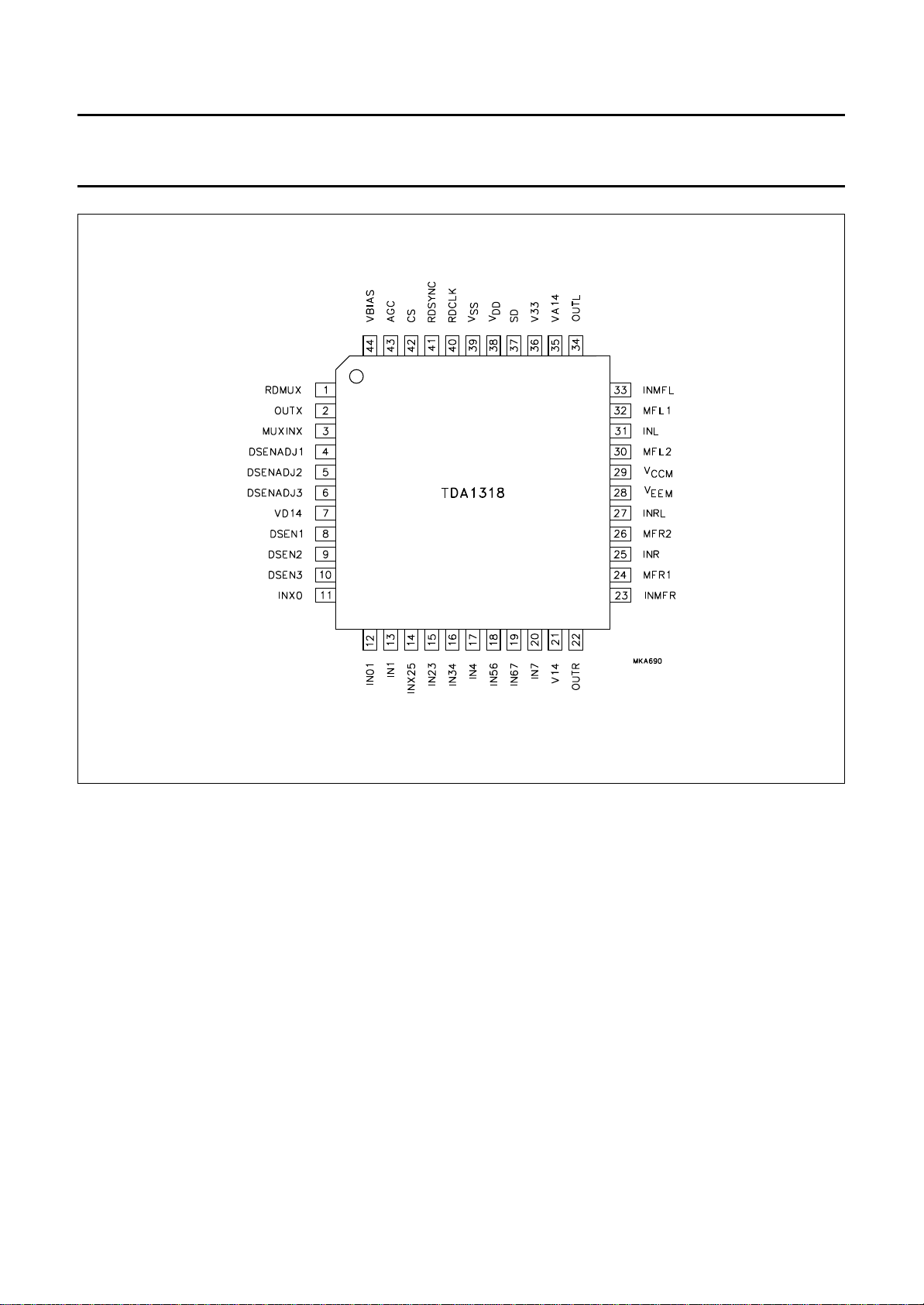
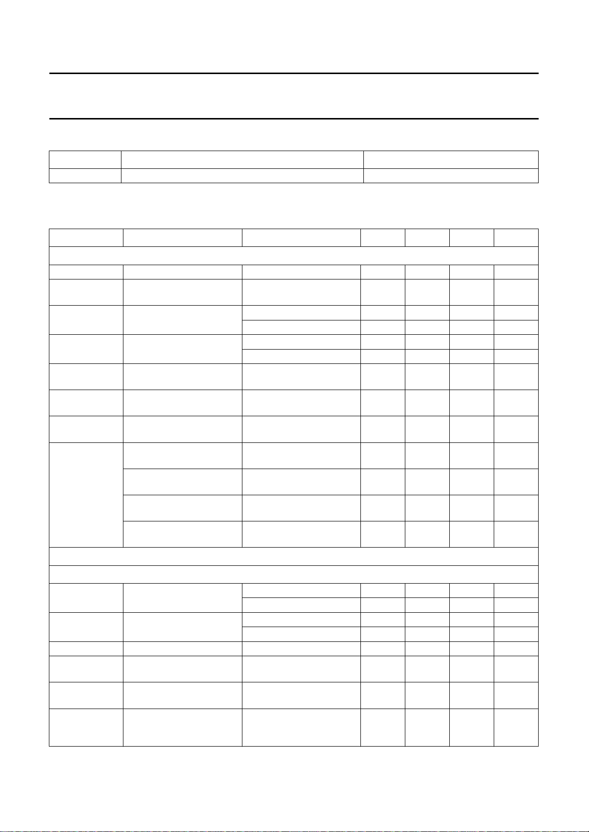
BLOCK DIAGRAM
PINS PIN POSITION MATERIAL CODE
PACKAGE
(1)
plastic SOT307-2
“Quality Reference Pocket
April 1996 3
Fig.1 Block diagram.
Philips Semiconductors Preliminary specification
DCC read amplifier TDA1318
PINNING
SYMBOL
PIN
DESCRIPTION
RDMUX 1 output for sampled and multiplexed
auxiliary and main data signals
OUTX 2 auxiliary channel preamplifier
output
MUXINX 3 auxiliary channel multiplexer input
DSENAD
J1
DSENAD
J2
DSENAD
J3
4 adjustment pin for DCC sense
current 1
5 adjustment pin for DCC sense
current 2
6 adjustment pin for DCC sense
current 3
VD14 7 reference voltage output DCC
sense
DSEN1 8 DCC sense current output 1
DSEN2 9 DCC sense current output 2
DSEN3 10 DCC sense current output 3
INX0 11 auxiliary channel input/channel 0
input
IN01 12 channels 0 and 1 input
IN1 13 channel 1 input
INX25 14 channels AUX, 2 and 5 input
IN23 15 channels 2 and 3 input
IN34 16 channels 3 and 4 input
IN4 17 channel 4 input
IN56 18 channels 5 and 6 input
IN67 19 channels 6 and 7 input
IN7 20 channel 7 input
V14 21 reference voltage output for
DCC/analog inputs
OUTR 22 right channel analog output
SYMBOL
PIN
DESCRIPTION
INMFR 23 right channel feedback amplifier
input
MFR1 24 right channel feedback amplifier
output 1
INR 25 right channel analog input
MFR2 26 right channel feedback amplifier
output 2
INRL 27 right/left channel analog input
V
V
EEM
CCM
28 ground for feedback amplifiers
29 positive supply for feedback
amplifiers
MFL2 30 left channel feedback amplifier
output 2
INL 31 left channel analog input
MFL1 32 left channel feedback amplifier
output 1
INMFL 33 left channel feedback amplifier
input
OUTL 34 left channel analog output
VA14 35 reference voltage output CC sense
V33 36 ADC reference voltage output
SD 37 select DCC part input
V
DD
V
SS
38 positive supply voltage
39 ground
RDCLK 40 read clock input
RDSYNC 41 read sync pulse input
CS 42 chip select input
AGC 43 AGC time constant
VBIAS 44 DCC preamplifier control voltage
April 1996 4
Philips Semiconductors Preliminary specification
DCC read amplifier TDA1318
Fig.2 Pin configuration.
FUNCTIONAL DESCRIPTION
DCC data amplifiers
For DCC operation the TDA1318 has eight channels for
the main data and one channel for the auxiliary data. The
eight main data channels have low-noise preamplifiers,
pre-equalisation for frequencies from 1 kHz to 50 kHz
(1st order high-pass filter, −3 dB point 75 kHz) and
low-pass filtering for anti-aliasing (2nd order active, −3dB
point 120 kHz). The auxiliary channel has a preamplifier
with a flat frequency response. A continuous output
(OUTX) is available for this channel. All inputs are
differential and must be AC-coupled to the MRHs. The
inputs are internally biased by V14.
Automatic gain control
The DCC part is equipped with an AGC circuit which
diminishes the gain of the DCC preamplifiers when the
level at output RDMUX exceeds a preset value.
April 1996 5
In this way, an optimum voltage swing at the RDMUX
output is obtained. The response time of the AGC can be
set by an external capacitor at pin 43. There is a fixed
relation between the source and sink current at this pin.
This results in a fixed relationship between decay and
recovery time of the gain. The AGC can be switched off by
connecting pin 43 to V
gains are maximum, as specified in Chapter
“Characteristics”.
Multiplexer
A multiplexing circuit switches the nine digital channels
sequentially to the output. The AUX data is switched to the
output buffer during two clock periods, the eight main data
channels are all sampled for one clock period. The
effective sample frequency is one tenth of the clock
frequency at RDCLK. Multiplexer timing is illustrated in
Fig.4.
. In this condition the preamplifier
SS
Philips Semiconductors Preliminary specification
DCC read amplifier TDA1318
Analog amplifiers
For Compact Cassette operation the TDA1318 has two
low-noise preamplifiers, and two amplifiers for the
magnetic feedback current. The analog amplifier inputs
are differential, and must be AC-coupled to the MRHs. The
analog inputs are internally biased by V14.
When one of the analog inputs, INL or INR, is connected
to VSS the circuit is set to the ADR mode. In this condition
the analog amplifiers are switched OFF and four DCC
preamplifiers are available for amplification of the left and
right analog signals.
Feedback amplifiers
Two feedback amplifiers are available for driving a coil in
the MRH, thus providing a feedback loop in order to
improve the linearity of the analog audio response. In the
DCC mode the feedback amplifiers can be used for biasing
the MRH (for ADR = 1).
Current and voltage sources
Separate, adjustable low-noise current sources are
present for the sense currents of the DCC MRHs.
The DC output voltages V14, VA14, VD14, and V33 are
derived from an internal bandgap voltage reference
source.
VD14 is a reference voltage for the DCC sense current
sources. VA14 (referenced to V
) can be used to control
SS
external sense current sources. V33 (referenced to VSS)
can be used as reference voltage for an analog-to-digital
converter.
Modes of operation
The amplifiers and sense current circuits of the DCC and
CC parts can be switched ON or OFF separately by the
mode switch signals CS and SD. In addition, a connection
of one of the analog inputs INL or INR to V
is recognized
SS
as the ADR mode, thereby providing amplification of audio
signals by the DCC preamplifiers. This enables the use of
heads containing only DCC readers as well as heads
equipped with analog and DCC readers.
The data and analog output buffers have high-output
impedance in the OFF state, thus allowing the outputs of
ICs to be connected in parallel.
Table 1 Total supply current per mode.
MODE CS SD ADR
TYP.
I
DD+ICCM
(mA)
IDD+I
MAX.
CCM
OFF 0 0 X <0.3 0.3
ADC reference only 0 1 X 1.6 2.2
CC 1 0 0 18.2 25.0
CC via DCC inputs 1 0 1 26.3 36.5
DCC (analog and digital readers) 1 1 0 31.0 41.0
DCC (digital readers only) 1 1 1 39.5 53.0
(mA)
April 1996 6
Philips Semiconductors Preliminary specification
DCC read amplifier TDA1318
Table 2 Modes of operation.
CONTROL
MODE
SIGNAL
CS SD ADR
DCC
PARTCCPARTFBAMPS
(1)
OFF 0 0 X off off off off OUTX; RDMUX;
ADC
REF
OUTPUTS
SWITCHED OFF
OUTPUTS
ENABLED
−
OUTL; OUTR
ADC reference only 0 1 X off off off on OUTX; RDMUX;
V33
OUTL; OUTR
CC 1 0 0 off on on off OUTX; RDMUX OUTL; OUTR
CC via DCC inputs 1 0 1 on
DCC (analog and digital
1 1 0 on off off on OUTL; OUTR V33; OUTX;
readers)
(2)
on
(3)
on off OUTX; RDMUX OUTL; OUTR
RDMUX
DCC (digital readers only) 1 1 1 on off on on OUTL; OUTR V33; OUTX;
RDMUX
Notes
1. ADR = 1 when pin INL and/or INR is connected to VSS.
2. Preamplifiers only; AGC disabled.
3. Output stages only; VA14 off.
LIMITING VALUES
In accordance with the Absolute Maximum Rating System (IEC 134).
SYMBOL PARAMETER CONDITIONS MIN. MAX. UNIT
V
V
DD
CCM
supply voltage VSS= 0; V
supply voltage feedback amplifiers −0.3 5.5 V
∆V difference in ground potential between V
V
I
I
EEM
I
CCM
I
n
I
DD
I
SS
I
max
P
tot
T
stg
T
amb
V
es
voltage on any pin VDD+ 0.5 < 5.5 V 0.3 VDD+ 0.5 V
maximum ground current (pin 28) −±120 mA
maximum supply current (pin 29) −±120 mA
maximum current on pins 24, 26, 30 and 32 −±80 mA
maximum supply current (pin 38) −±80 mA
maximum ground current (pin 39) −±80 mA
maximum current on all other pins −±20 mA
total power dissipation − 350 mW
storage temperature −65 +150 °C
operating ambient temperature −30 +85 °C
electrostatic handling −2000 +2000 V
and V
SS
EEM
=0 −0.3 5.5 V
EEM
00V
April 1996 7
Philips Semiconductors Preliminary specification
DCC read amplifier TDA1318
THERMAL RESISTANCE
SYMBOL PARAMETER THERMAL RESISTANCE
R
th j-a
CHARACTERISTICS
= 5 V; V
V
DD
SYMBOL PARAMETER CONDITIONS MIN. TYP. MAX. UNIT
Supply
V
DD
V
CCM
I
DDDCC
I
DDCC
I
CCM
I
DD
I
tot
V
ref
from junction to ambient in free air 90 K/W
= 5 V; VSS=V
CCM
EEM
= 0 V; f
= 3.072 MHz; T
clk
=25°C; unless otherwise specified.
amb
supply voltage 4.5 5.0 5.5 V
supply voltage feedback
4.5 5.0 5.5 V
amplifiers
supply current DCC part CS = 1; SD = 1; ADR = 0 21 31 41 mA
CS = 1; SD = 1; ADR = 1 21 31 41 mA
supply current CC
amplifiers
supply current feedback
CS = 1; SD = 0; ADR = 0 7 9.7 13 mA
CS = 1; SD = 0; ADR = 1 12.5 17.8 24.5 mA
note 1 6.0 8.5 12 mA
amplifiers
supply current
CS = 0; SD = 1 1.1 1.6 2.2 mA
(ADC reference ON)
total current in OFF state
of IDD and I
CCM
reference voltage for DCC
CS = 0; SD = 0 −−300 µA
Io< −1 mA 1.3 1.4 1.5 V
inputs (pin 21)
reference voltage for DCC
I
< −20 µA 1.25 1.4 1.55 V
o
sense (pin 7)
reference voltage for CC
< −20 µA 1.25 1.4 1.6 V
I
o
sense (pin 35)
reference voltage for ADC
< −2.5 mA 3.2 3.3 3.4 V
I
o
(pin 36)
DCC part
MPLIFIER CHANNEL 0 TO 7; NOTE 2
A
G amplifier gain f
∆G relative gain f
V
O
V
os
DC output voltage note 4 1.8 2.1 2.4 V
DC offset voltage between
channels
V
n(ref)
input referred noise
voltage
∆V
n(ref)
3 × standard deviation in
amplitude spread of input
referred noise
April 1996 8
= 50 kHz 75 78 81 dB
i
= 100 kHz 75 80 83 dB
f
i
= 10 kHz; note 3 −14 −12 −10 dB
i
= 300 kHz; note 3 −22 −12 −3dB
f
i
note 4 −−300 mV
fi= 50 kHz; R
fi= 50 kHz; R
=70Ω− 1.9 − nV√Hz
source
=70Ω− 0.5 − nV√Hz
source
 Loading...