

Philips TDA1315H-N2 Datasheet

DATA SH EET
Product specification
Supersedes data of December 1994
File under Integrated Circuits, IC01
1995 Jul 17
INTEGRATED CIRCUITS
TDA1315H
Digital audio input/output circuit
(DAIO)
1995 Jul 17 2
Philips Semiconductors Product specification
Digital audio input/output circuit (DAIO) TDA1315H
FEATURES
• Transceiver for SPDIF and
“IEC 958”
encoded signals
• High sensitivity input for transformer-coupled links
• TTL-level input for optical links
• Built-in IEC input selector
• Built-in IEC feed-through function
• Automatic sample frequency (fs) detection
• System clock recovery from IEC input signal
• Low system clock drift when IEC input signal is removed
• Error detection and concealment
• PLL lock detection in transmit mode
• Serial audio interface conforms to I
2
S-bus format
• Auxiliary I2S-bus input for Analog-to-Digital Converter
(ADC)
• Audio output selector
• Microcontroller-controlled and stand-alone mode
• 128-byte buffer for user data
• Bytewise exchange of user data with microcontroller
• Decoding of Compact Disc (CD) subcode Q-channel
data
• Support for serial copy management system (SCMS)
• Light Emitting Diode (LED) drive capability
(sample frequency and error indication)
• Pin-selectable device address for
microcontroller interface
• Power-down mode.
GENERAL DESCRIPTION
The Digital Audio Input/Output circuit (DAIO) of the
TDA1315H is a complete transceiver for biphase-mark
encoded digital audio signals that conform to the SPDIF
and
“IEC 958”
interface standards (consumer mode),
made in the full CMOS-process C200.
In the receive mode, the device adjusts automatically to
one of the three standardized sample frequencies
(32, 44.1 or 48 kHz), decodes the input signal and
separates audio and control data. A clock signal of either
256 or 384 times the sample frequency is generated to
serve as a master clock signal in digital audio systems.
In the transmit mode, the device multiplexes the audio
control and user data and encodes it for subsequent
transmission via a cable or optical link.
ORDERING INFORMATION
TYPE
NUMBER
PACKAGE
NAME PIN POSITION VERSION
TDA1315H QFP44 plastic quad flat package; 44 leads (lead length 1.3 mm);
body 10 × 10 × 1.75 mm
SOT307-2
1995 Jul 17 3
Philips Semiconductors Product specification
Digital audio input/output circuit (DAIO) TDA1315H
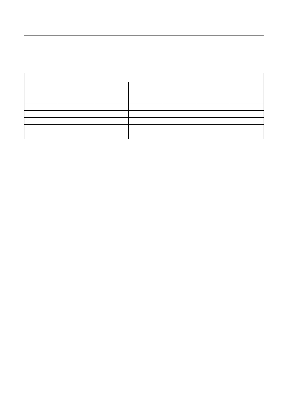
QUICK REFERENCE DATA
All inputs are TTL compatible; all outputs are CMOS compatible; unless otherwise specified.
SYMBOL PARAMETER CONDITIONS MIN. TYP. MAX. UNIT
Supply
V
DD
supply voltage V
DDD=VDDA
3.4 5.0 5.5 V
I
DDAq
analog quiescent current PD = 1; T
amb
=25°C −−10 µA
I
DDDq
digital quiescent current PD = 1; T
amb
=25°C −−10 µA
I
DDA
analog supply current fs= 48 kHz; CLKSEL = 0;
when IECIN1 input is used
− 2.6 − mA
I
DDD
digital supply current fs= 48 kHz; CLKSEL = 0 − 13 − mA
Power
P
tot
total power dissipation fs= 48 kHz; CLKSEL = 0;
when IECIN1 input is used
− 80 − mW
Temperature
T
amb
operating ambient temperature −20 − +70 °C
IEC interface; pin IECIN1 (high sensitivity IEC input)
V
i(p-p)
AC input voltage
(peak-to-peak value)
0.2 − V
DD
V
Control part
CHMODE, UNLOCK,
FS32, FS44, FS48 AND COPY (OPEN-DRAIN OUTPUTS)
V
OL
LOW level output voltage IOL= 3 mA −−0.5 V
RESET, SCK, LCLK, LMODE AND SYSCLKI (HYSTERESIS INPUTS)
V
tHL
negative-going threshold VDD= 4.5 to 5.5 V 0.6 −−V
V
tLH
positive-going threshold VDD= 4.5 to 5.5 V −−2.4 V
V
hys
input voltage hysteresis VDD= 4.5 to 5.5 V − 0.7 − V
Clock and timing
V
ref
output reference voltage − 2.1 − V
RC
int
(PIN 44)
I
CHfr
charge-pump output current frequency detector loop −±12 −µA
I
CHph
charge-pump output current phase detector loop −±24 −µA

1995 Jul 17 4
Philips Semiconductors Product specification
Digital audio input/output circuit (DAIO) TDA1315H
BLOCK DIAGRAM
Fig.1 Block diagram.
1995 Jul 17 5
Philips Semiconductors Product specification
Digital audio input/output circuit (DAIO) TDA1315H
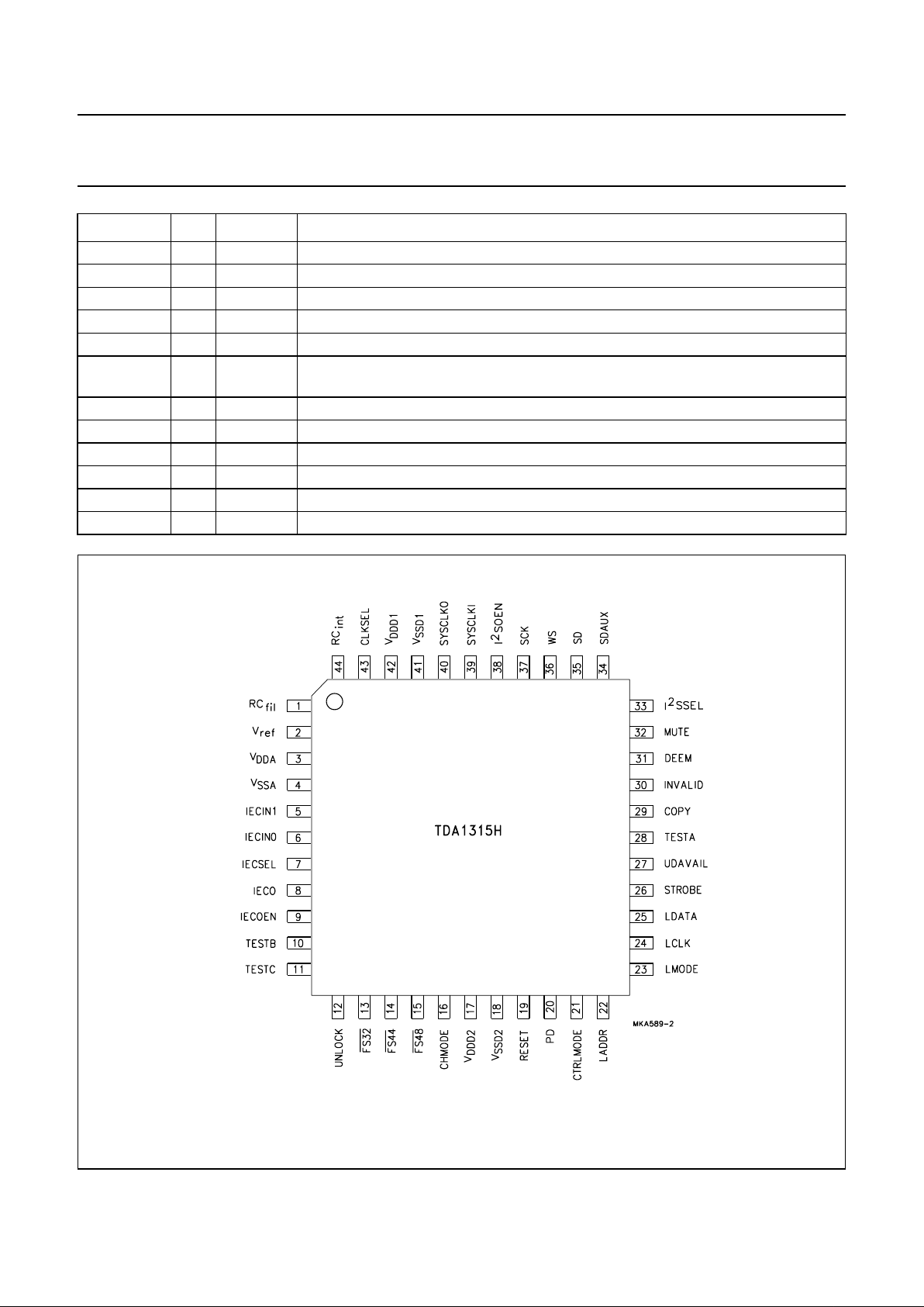
PINNING
SYMBOL PIN PADCELL DESCRIPTION
RC
fil
1 E029 PLL loop filter input
V
ref
2 E029 decoupling internal reference voltage output
V
DDA
3 E008 analog supply voltage
V
SSA
4 E004 analog ground
IECIN1 5 E007 high sensitivity IEC input
IECIN0 6 IPP04 TTL level IEC input
IECSEL 7 IUP04 select IEC input 0 or 1 (0 = IECIN0; 1 = IECIN1); this input has an internal pull-up
resistor
IECO 8 OPFH3 digital audio output for optical and transformer link
IECOEN 9 IUP04 digital audio output enable (0 = enabled; 1 = disabled/3-state); this input has an
internal pull-up resistor
TESTB 10 IPP04 enable factory test input (0 = normal application; 1 = scan mode)
TESTC 11 IPP04 enable factory test input (0 = normal application; 1 = observation outputs)
UNLOCK 12 OPP41A PLL out-of-lock (0 = not locked; 1 = locked); this output can drive an LED
FS32 13 OPP41A indicates sample frequency = 32 kHz (active LOW); this output can drive an LED
FS44 14 OPP41A indicates sample frequency = 44.1 kHz (active LOW); this output can drive an LED
FS48 15 OPP41A indicates sample frequency = 48 kHz (active LOW); this output can drive an LED
CHMODE 16 OPP41A use of channel status block (0 = professional use; 1 = consumer use); this output
can drive an LED
V
DDD2
17 E008 digital supply voltage 2
V
SSD2
18 E009 digital ground 2
RESET 19 IDP09 initialization after power-on, requires only an external capacitor connected to V
DDD
;
this is a Schmitt-trigger input with an internal pull-down resistor
PD 20 IPP04 enable power-down input in the standby mode (0 = normal application; 1 = standby
mode)
CTRLMODE 21 IUP04 select microcontroller/stand-alone mode (0 = microcontroller; 1 = stand-alone); this
input has an internal pull-up resistor
LADDR 22 IPP04 microcontroller interface address switch input (0 = 000001; 1 = 000010)
LMODE 23 IPP09 microcontroller interface mode line input
LCLK 24 IPP09 microcontroller interface clock line input
LDATA 25 IOF24 microcontroller interface data line input/output
STROBE 26 IDP04 strobe for control register (active HIGH); this input has an internal pull-down resistor
UDAVAIL 27 OPF23 synchronization for output user data (0 = data available; 1 = no data)
TESTA 28 IPP04 enable factory (scan) test input (0 = normal application; 1 = test clock enable)
COPY 29 OPP41A copyright status bit (0 = copyright asserted; 1 = no copyright asserted); this output
can drive an LED
INVALID 30 IOD24 validity of audio sample input/output (0 = valid sample; 1 = invalid sample); this pin
has an internal pull-down resistor
DEEM 31 OPF23 pre-emphasis output bit (0 = no pre-emphasis; 1 = pre-emphasis)
MUTE 32 IUP04 audio mute input (0 = permanent mute; 1 = mute on receive error); this pin has an
internal pull-up resistor
1995 Jul 17 6
Philips Semiconductors Product specification
Digital audio input/output circuit (DAIO) TDA1315H
I2SSEL 33 IUP04 select auxiliary input or normal input in transmit mode
SDAUX 34 IPP04 auxiliary serial data input; I
2
S-bus
SD 35 IOF24 serial audio data input/output; I
2
S-bus
WS 36 IOF24 word select input/output; I
2
S-bus
SCK 37 IOF29 serial audio clock input/output; I
2
S-bus
I
2
SOEN 38 IUP04 serial audio output enable (0 = enabled; 1 = disabled/3-state); this input has an
internal pull-up resistor
SYSCLKI 39 IPP09 system clock input (transmit mode)
SYSCLKO 40 OPFA3 system clock output (receive mode)
V
SSD1
41 E009 digital ground 1
V
DDD1
42 E008 digital supply voltage 1
CLKSEL 43 IUP04 select system clock (0 = 384f
s
; 1 = 256fs); this input has an internal pull-up resistor
RC
int
44 E029 integrating capacitor output
SYMBOL PIN PADCELL DESCRIPTION
Fig.2 Pin configuration.

1995 Jul 17 7
Philips Semiconductors Product specification
Digital audio input/output circuit (DAIO) TDA1315H
FUNCTIONAL DESCRIPTION
Modes of operation
With respect to the control of the device and the exchange
of non-audio data, a microcontroller (host) mode and a
stand-alone mode can be considered. The selection of the
mode is performed at pin CTRLMODE.
In the stand-alone mode, the device configuration is solely
determined by pins. In the host mode an internal control
register, or pins or both can be used to change the default
settings.
With respect to the direction of the digital audio data, the
device can be operated in either a transmit or a receive
mode under control of a microcontroller. In the stand-alone
mode the device is only a receiver. In the receive mode the
input signal can also be made available at the output pin
IECO (feed-through) to ease the cascading of digital audio
equipment.
The device can be brought to standby mode at all times by
activating the PD pin (power down). In this mode all
functions are disabled, all outputs 3-stated, supply current
is minimized and the contents of the register are saved.
General
For those applications where it is important to save power,
the PD pin is provided, which, when activated, puts the
TDA1315H in standby mode by disabling all functions and
3-stating all outputs, while saving register contents.
As illustrated in Fig.1, the TDA1315H contains the
following major functional blocks:
• IEC input section
• Biphase demodulator
• Frame and error detection
• Clock and timing section
• IEC output section
• Biphase modulator
• Audio section (I
2
S-bus transceiver)
• Non-audio section (control and FIFO)
• User (microcontroller) interface.
IEC
INPUT SECTION
There are two biphase signal inputs to the IEC input
section. IECIN0 accepts TTL levels from, for example, an
optical input device, while IECIN1 is designed for coaxial
cable inputs and requires signal levels of minimum
200 mV (p-p) via an external coupling capacitor. The
selection of the active input channel is performed by pin
IECSEL or by the control register or both. In the receive
mode, the selected input signal is applied internally to the
biphase audio output section to enable a feed-through
function.
B
IPHASE DEMODULATOR
In the biphase demodulator, the received signal (for details
see Chapter “References”[1] and [2]) is converted to
binary data and separated into audio and non-audio data
for further processing in their dedicated sections. The
demodulated input signal is also required for frame and
error detection.
F
RAME AND ERROR DETECTION
In the frame and error detection block, the framing
information from the received biphase signal is retrieved to
synchronize the biphase demodulator and to allow access
to the audio and non-audio data bits. An out-of-lock
condition of the PLL is flagged at UNLOCK. The validity of
audio samples is indicated at pin INVALID.
C
LOCK AND TIMING SECTION
In the clock and timing section, the timing information
inherent to the received biphase signal is retrieved and a
symmetrical master clock signal is generated and output at
pin SYSCLKO. Depending on the mode of operation, the
frequency of this master clock can be selected by pin
CLKSEL, by the control register or both to be either 256f
s
or 384fs (fs= audio sampling frequency). This section
contains all the circuitry of a Phase-Locked Loop (PLL),
except for the loop filter components, which are connected
externally to pins RC
int
and RC
fil
. When the input signal is
interrupted, the oscillator will slowly drift to the
centre frequency in order to keep the system operating on
a proper frequency. In the transmit mode, all required
timing signals are input at pin SYSCLKI and are derived
from an externally supplied system clock of either 256fs or
384fs. The input HIGH time of that clock may be in the
range between 30% to 70% of the clock period.
IEC
OUTPUT SECTION
In the IEC output section, either the received (feed-through
function) or the generated biphase signal is selected for
output at pin IECO, depending on the receive/transmit
mode. The output can be enabled/disabled by pin
IECOEN, by the control register or both, and can drive a
suitable optocoupler and a transformer in parallel.

1995 Jul 17 8
Philips Semiconductors Product specification
Digital audio input/output circuit (DAIO) TDA1315H
BIPHASE DEMODULATOR
In the biphase modulator section, audio and non-audio
data are combined into subframes, frames and blocks, and
encoded in the biphase-mark format during transmit mode.
Although there are always 24 audio bits per sample in a
subframe, the number of significant bits can be selected as
16, 18, 20 or 24 via the control register (host mode).
A
UDIO SECTION
In the audio section, the left and right channel audio
samples are taken from the demodulated data frames and
are output serially in accordance with the I2S-bus format
(for details see Chapter “References”[3] pins SD, SCK and
WS) when the TDA1315H is in the receive mode (I2S-bus
transmitter). The audio output signals are concealed or
muted in case certain errors were detected during
reception. Mute can be enforced by pin MUTE or via the
control register (host mode) and affects, depending on the
receive/transmit mode, the I2S-bus or IEC output signals.
MUTE is internally synchronized with the audio data. In the
transmit mode, there is an additional I2S-bus data input
SDAUX made available to accept audio data from, for
example, an ADC. This input can be selected either by pin
I2SSEL, by the control register or both. The I2S-bus Port
can be enabled/disabled by pin I2SOEN, by the control
register or both. In the transmit mode, I2S-bus data and
timing are supplied by an external source, the TDA1315H
then becomes an I2S-bus receiver. In this event, selection
of an I2S-bus source determines which signal is to be
output at IECO. Although the phase relationship between
system clock (SYSCLKI) and I2S timing (SCK) is not
critical they must be synchronous with each other, i.e. be
derived from the same source.
Receive mode
The IEC subframe format defines 20 bits for an audio
sample, plus 4 auxiliary bits, which can be used to extend
the word length. By default, all 24 data bits per sample are
output via the I2S-bus Port. This can be changed,
however, to 16, 18 or 20 bits via bits 2 and 3 in byte 1 of
the control register. The remaining bits will then be zero.
The serial audio clock frequency at pin SCK is 64 × fs, i.e.
there are 32 clock pulses per audio sample (left or right
channel).
Apart from detecting the out-of-lock condition of the PLL,
received data is checked for the errors listed below. All
detected errors will be flagged in the status register and
two of them brought out to a pin. Depending on the type of
error, different measures are taken.
• Validity flag set. This error condition is also output at pin
INVALID, simultaneously with the data. The
corresponding audio sample is not modified.
• Parity check error. A concealment operation is
performed on both audio channels (left and right), i.e.
the last correctly received stereo sample is output again.
• Biphase violation (other than preambles). A
concealment operation (hold) is performed on both
audio channels (left and right), i.e. the last correctly
received stereo sample is output again.
• PLL is out-of-lock. This error condition is also output at
pin UNLOCK. Both audio output channels (left and right)
are set to zero (mute). The error condition is sampled
with the HIGH-to-LOW transition of WS, i.e. muting
becomes effective when the outputting of a stereo
sample begins. When the PLL has locked again, muting
is released only after a full block of audio samples has
been received, free of errors.The INVALID output will
always be set to LOW simultaneously with this muting.
In the receive mode it is possible to select the auxiliary
I
2
S-bus data input SDAUX for output at pin SD. However,
there will be no suitable system clock available in the event
of an open IEC input or a disabled IEC source and output
SD will be muted when the TDA1315H is not in lock.
Regardless of which source is selected, a MUTE
command will always mute the output signal at pin SD and
set the INVALID output to LOW regardless of the validity
bit value. When mute command is disabled, muting will be
released when the outputting of the next stereo sample
begins.
1995 Jul 17 9
Philips Semiconductors Product specification
Digital audio input/output circuit (DAIO) TDA1315H
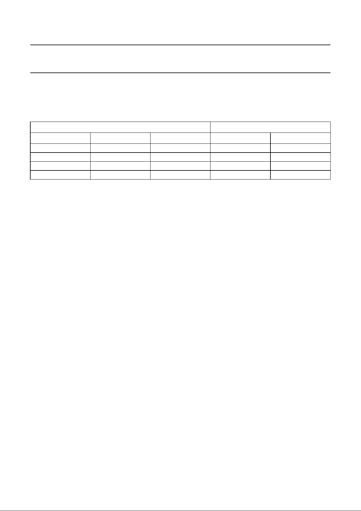
Table 1 Summary of validity and muting in the receive mode
Note
1. X = don’t care.
INPUT CONDITIONS
(1)
OUTPUTS
PLL LOCKED
MUTE
ACTIVATED
SDAUX
SELECTED
I2SOUT
ENABLED
VALIDITY BIT INVALID SD
X X X no X 3-state 3-state
No X X yes X 0 0
X yes X yes X 0 0
Yes no no yes 0 0 IEC
Yes no no yes 1 1 IEC
Yes no yes yes X 0 SDAUX
When the I2S-bus output Port is disabled by pin I2SOEN in
the stand-alone mode, pins WS, SCK, SD and INVALID
will immediately become 3-state. If, however, this is
performed in the host mode via the I2SOEN pin or the
corresponding bit in the control register, only SD and
INVALID will become 3-state immediately. Pins WS and
SCK will only become 3-state after the rising edge of
STROBE when the STROBE pulse changes the setting
from receive to transmit mode. Thus in the host mode,
when remaining in the receive mode, I2SOEN only
influences the SD and INVALID pins. Pins WS and SCK
are always enabled. When the I2S-bus output Port is
re-enabled, data output will start with the beginning of a
new stereo sample.
Transmit mode
Although the IEC subframe format supports up to 24 bits
per audio sample, the number of significant bits can be
selected as 16, 18, 20 or 24 via the control register.
Because the I2S-bus Port then operates as a receiver, the
timing has to be selected so that all data bits can be
received. Any bits unused or unsupplied will be set to
logic 0.
The information regarding audio samples that may be
unreliable or invalid has to be entered at pin INVALID
simultaneously with the data input to pin SD. The timing
will be the same as in the CD decoder ICs (e.g. the EFAB
signal of the SAA7310, see Chapter “References”[5].
As the I2S-bus Port is used as an input, it must be disabled
by the correct combination of pin I2SOEN and the
corresponding bit in the control register. The pins WS and
SCK are set to 3-state on the rising edge of STROBE,
whenever the transmit mode is activated. I2SOEN
influences only the data pin SD. This allows for three
different configurations:
• Transmit mode #1, I
2
SOEN = 1, I2SSEL = 1. In this
instance, I2S-bus timing and data are derived from an
external source and entered at pins WS, SCK and SD.
Output will be at pin IECO, if IECOEN permits.
• Transmit mode #2, I2SOEN = 1, I2SSEL = 0. In this
instance, I2S-bus timing is derived from an external
source and entered at pins WS and SCK and is also
supplied to another I2S-bus source, such as an ADC.
Data from that other I2S-bus source is entered at pin
SDAUX. Output will be at pin IECO, if IECOEN permits.
In this instance, I2SSEL acts as a source selector for
pins SD and SDAUX.
• Transmit mode #3, I2SOEN = 0, I2SSEL = 0. In this
instance, I2S-bus timing is derived from an external
source and entered at pins WS and SCK and is also
supplied to another I2S-bus source, such as an ADC.
Data from the other I2S-bus source is entered at pin
SDAUX. Output will be at pin IECO, if IECOEN permits,
and at pin SD. In this mode, SDAUX data is available
both at the IEC output (a type of digital monitor function)
and on the I2S-bus (e.g. for digital signal processing
purposes).
The remaining combination (I2SOEN = 0, I2SSEL = 1) is
not used. WS, SCK and SD are then 3-state.
Because the SDAUX input normally receives a signal from
an ADC, the signal at pin INVALID will not be interpreted
when this input is selected. All samples are assumed to be
valid. In all transmit modes, INVALID is an input pin.
1995 Jul 17 10
Philips Semiconductors Product specification
Digital audio input/output circuit (DAIO) TDA1315H
Whenever MUTE is activated in any of the transmit modes, the audio data of the IEC output signal will be muted and the
validity bit set to logic 0, regardless of the INVALID input value. When SDAUX is selected, MUTE will also affect the
output at pin SD.
Table 2 Summary of validity and muting in the transmit mode
Note
1. X = don’t care.
INPUT CONDITIONS
(1)
IEC OUTPUT SIGNAL
MUTE ACTIVATED SDAUX SELECTED INVALID INPUT VALIDITY BIT AUDIO BITS
No no 0 0 from SD
No no 1 1 from SD
No yes X 0 from SDAUX
Yes X X 0 0
NON-AUDIO SECTION
In the non-audio section, the first 30 channel status bits
are taken from each block of data. A selection of 16 bits is
then assembled as two bytes and transferred to the user
interface. In the event of an incorrect IEC signal, i.e. no
consumer mode, an error will be flagged at pin CHMODE.
The error signal will return to its passive state after a full
block of consumer mode data has been received. The user
data bits are searched for the beginning of a ‘message’
(see Section “User data”), which is then stored bytewise in
a buffer that can be read by an external microcontroller via
the user interface. In the transmit mode, channel status
and user data bits are taken from an internal buffer that
has been written to by an external microcontroller via the
user interface. These bits are required for frame
composition in the biphase modulator.
The non-audio section supports only the consumer mode
of the
“IEC 958”
specification and handles the channel
status and user data information.
The non-audio section can be operated in the stand-alone
mode (receive only) and the host mode (transmit/receive).
In the stand-alone mode, a few bits from the channel
status are brought out to pins, the user data is not
available. In the host mode, channel status and user data
are exchanged using a microcontroller. After a RESET in
the host mode, the TDA1315H provides general format by
default.
Channel status
The channel status consists of 30 bits, a number of which
are reserved for future standardization. The 16 most
significant bits (MSBs), arranged as two bytes, are
exchanged using an external microcontroller. The
mapping of the channel status bits into these two bytes is
given in Tables 3 and 4. All SCMS operations (Serial Copy
Management System) will be performed in the
microcontroller and no manipulation in the TDA1315H is
possible. Bit 0 is always the first bit on the user interface.
In the receive mode, an error signal is generated at pin
CHMODE if a professional mode signal is received. Even
then, two bytes of information, mapped as defined in
Tables 3 and 4, are generated for output. Although there
are two bytes of channel status available for output, only
the first byte can be read. To identify future modes of the
channel status, both mode bits (bits 6 and 7 in the channel
status) are available (inverted) from the TDA1315H status
register. The channel status is created from the left
channel subframes of the IEC signal (preambles ‘B’
and ‘M’).
Whenever the channel status, as defined in
Tables 3 and 4 (16 bits), differs from the previously
received channel status, a bit will be set in the TDA1315H
status register. This helps to reduce the data traffic by
enabling the microcontroller to read the channel status
only after it has changed.
In the transmit mode, the microcontroller supplies
consumer mode (Mode 0) channel status data as
described in Table 3. Both bytes need to be transferred.

1995 Jul 17 11
Philips Semiconductors Product specification
Digital audio input/output circuit (DAIO) TDA1315H
Table 3 First byte of transferred channel status
Table 4 Second byte of transferred channel status
User data
In principle, the user data bits may be used in any way
required by the user. In order to guarantee compatibility
between signals of any source, attempts have been made
for the standardization of a user data format. The basic
idea is to transfer ‘messages’ that consist of ‘information
units’. As messages are, typically, asynchronous with the
IEC audio block structure, their transfer relies on software
protocol. Currently, the applications for CD subcode and
DAT have been accepted. Their general format complies
with that protocol and can be described as follows:
• User data is transferred in the form of messages.
• Messages consist of information units, i.e. groups of
8 bits (bytes).
• Messages are separated by more than 8 zero bits (0).
• Information units within a message may be separated by
0 up to and including 8 zero bits.
• The MSB of each byte is sent first in the user data
channel.
• The MSB of each byte is a 1-bit (1, start bit).
• For CD subcode, one byte consists of bits 1QRSTUVW.
BIT DESCRIPTION
BIT IN
CHANNEL
STATUS
0 and 1 clock accuracy 29 and 28
2 and 3 sample frequency 25 and 24
4 pre-emphasis 3
5 copyright 2
6 audio/data 1
7 consumer/professional use 0
BIT DESCRIPTION
BIT IN
CHANNEL
STATUS
0 category code 15
1 category code 14
2 category code 13
3 category code 12
4 category code 11
5 category code 10
6 category code 9
7 category code 8
Normally, the exchange of user data between the
TDA1315H and the microcontroller is based on the
general format described above. In the event of CD
subcode, this means that 96 bytes need to be transferred
for each subcode frame. In order to reduce the amount of
data traffic, it is possible to separate the Q-channel bits
from the user data and transfer only them. This mode can
be enabled by a bit in the control register and leads to the
transfers of only 12 bytes per subcode frame. As there is
no check in the TDA1315H whether user data is from a CD
source, this Q-channel decoding can be employed
whenever the user data format permits.
Receive mode
User data bits are extracted from the received IEC
subframes and searched for the beginning of a message.
When Q-channel decoding is disabled (in the control
register), the data bytes of a message are stored in a
buffer for subsequent external interpretation or
processing. Any 0 bits between information units and
between messages are skipped.
It is essential to maintain synchronization of messages,
even if not all bytes of a message can be exchanged with
the microcontroller in a single transfer, or if there are
several messages in the buffer. When user data is
transferred in the general format described earlier, the
beginning of a message is indicated in the buffer by a 1 bit
in the MSB position of the first byte of that message. In all
subsequent bytes of the same message, the MSB will be
zero. This is illustrated in Table 5 for the CD subcode.
The user data buffer is implemented as a FIFO (First-In,
First-Out) with a size of 128 bytes. This allows the storing
of a full CD subcode frame. A synchronization signal at pin
UDAVAIL supports the transfer of user data to the
microcontroller. This signal goes LOW when there is at
least 1 byte of user data in the buffer, and returns HIGH
only after the last received byte has been read. This is
illustrated in Fig.3.
Based on the timing of the CD subcode, the
microcontroller should start reading data within 17 ms after
UDAVAIL has gone LOW, otherwise the buffer will fill
completely and the most recent data will be lost.
 Loading...