

Philips TDA1314T Datasheet

Philips Semiconductors Product specification
Quadruple filter DAC TDA1314T
FEATURES
• High dynamic range to enable digital DSP (Digital Signal
Processor) volume control
APPLICATIONS
• Stand-alone quadruple low noise DAC
• Car radio DAC in conjunction with DSP.
• 18 bits data input format for each of the four channels
• Four times bit-serial oversampling filter
• 1st-order 4fas (audio sampling frequency) noise shaper
• Four very low noise DACs
• Only 1st-order analog post filtering required
• Smooth power-on of the DAC output currents
• Because of the automatic digital PLL divider range
setting the master clock is selectable in a wide 4f
as
integer range
GENERAL DESCRIPTION
The TDA1314T is a quadruple very low noise high
dynamic range DAC which is intended for use in motor
cars and is controlled by the car radio DSP. Each channel
incorporates an 8th-order IIR up-sampling filter from 1ASF
to 4ASF followed by a 1st-order noise shaper and DAC.
The DAC currents are converted to audio voltage signals
using operational amplifiers (one per channel).
• Insensitive to jitter on the I2S-bus signals with respect to
the DAC total harmonic distortion deterioration.
QUICK REFERENCE DATA
V
= 2.5 and 5 V; T
ref
= 25 °C; all voltages referenced to ground; unless otherwise specified.
amb
SYMBOL PARAMETER CONDITIONS MIN. TYP. MAX. UNIT
V
DDA
V
DDD
I
O(DAC)
V
O(DAC)
analog supply voltage 4.5 5.0 5.5 V
digital supply voltage 4.5 5.0 5.5 V
DAC output current (FS) R
DAC output voltage,
= 20.5 kΩ ±0.4 ±0.5 ±0.6 mA
ref
RL≥ 5 kΩ; Rfb= 3 kΩ 1.0 − 4.0 V
nominal DAC operational
amplifier output voltage
RES DAC resolution length of data input word − − 18 bits
(THD + N)/S total harmonic distortion
plus noise-to-signal ratio
DR dynamic range of DAC fi= 1 kHz;
fi= 1 kHz;
0 dB signal level
− −66 −56 dB
92 96 − dB
−60 dB signal level
DS digital silence no signal; A-weighted − −110 −100 dB
P
tot
T
amb
total power dissipation − 85 − mW
operating ambient
−40 +25 +85 °C
temperature
ORDERING INFORMATION
TYPE NUMBER
NAME DESCRIPTION VERSION
PACKAGE
TDA1314T SO28 plastic small outline package; 28 leads; body width 7.5 mm SOT136-1
August 1994 2
Philips Semiconductors Product specification
handbook, full pagewidth
MBE001
20 20
5
20-bit
DATA WORD
LATCH
NOISE
SHAPER
15
15-bit
DATA WORD
LATCH
5
THERM.
DEC.
9
MSB
1 2 3 31 32
COARSE CURRENT SOURCES
I
ref
FINE
CURRENT
MATRIX
CURRENT
DIRECTION
SWITCH
I
out-f
I
out-c
DAC LATCH
I
out
DAC FL
4 f
UP-SAMPLE
FILTER
s
4 f
s
4 f
UP-SAMPLE
FILTER
s
4 f
UP-SAMPLE
FILTER
s
4 f
UP-SAMPLE
FILTER
s
NOISE
SHAPER
DAC
LATCH
DAC FR
NOISE
SHAPER
DAC
LATCH
DAC RL
NOISE
SHAPER
DAC
LATCH
DAC RR
181818
18
I S
INTERFACE
2
10
11
I
ORR
V
ORR
12
13
I
ORL
V
ORL
17
18
I
OFR
V
OFR
19
20
I
OFL
V
OFL
R
ref
V
ref
21
14
16 15
OGND
229876
POWER-UP
V
DDA
V
DDO
V
DDD
AGNDDGND
TEST
INTERFACE
test
signals
UP-SAMPLE
CLOCK GENERATOR
SYNTHESIZER
DIVIDED BY 45 . . . 128
5
3
4 ASF GENERATOR
FASF DAC
UPSAMPLE
CLOCKS
23
MCLK
SELINPH
WS
SCK
SDF
SDR
26425
24
AT/DT
TC
SCOUT1
SCOUT2
2
1
27
28
CMT
TDA1314T
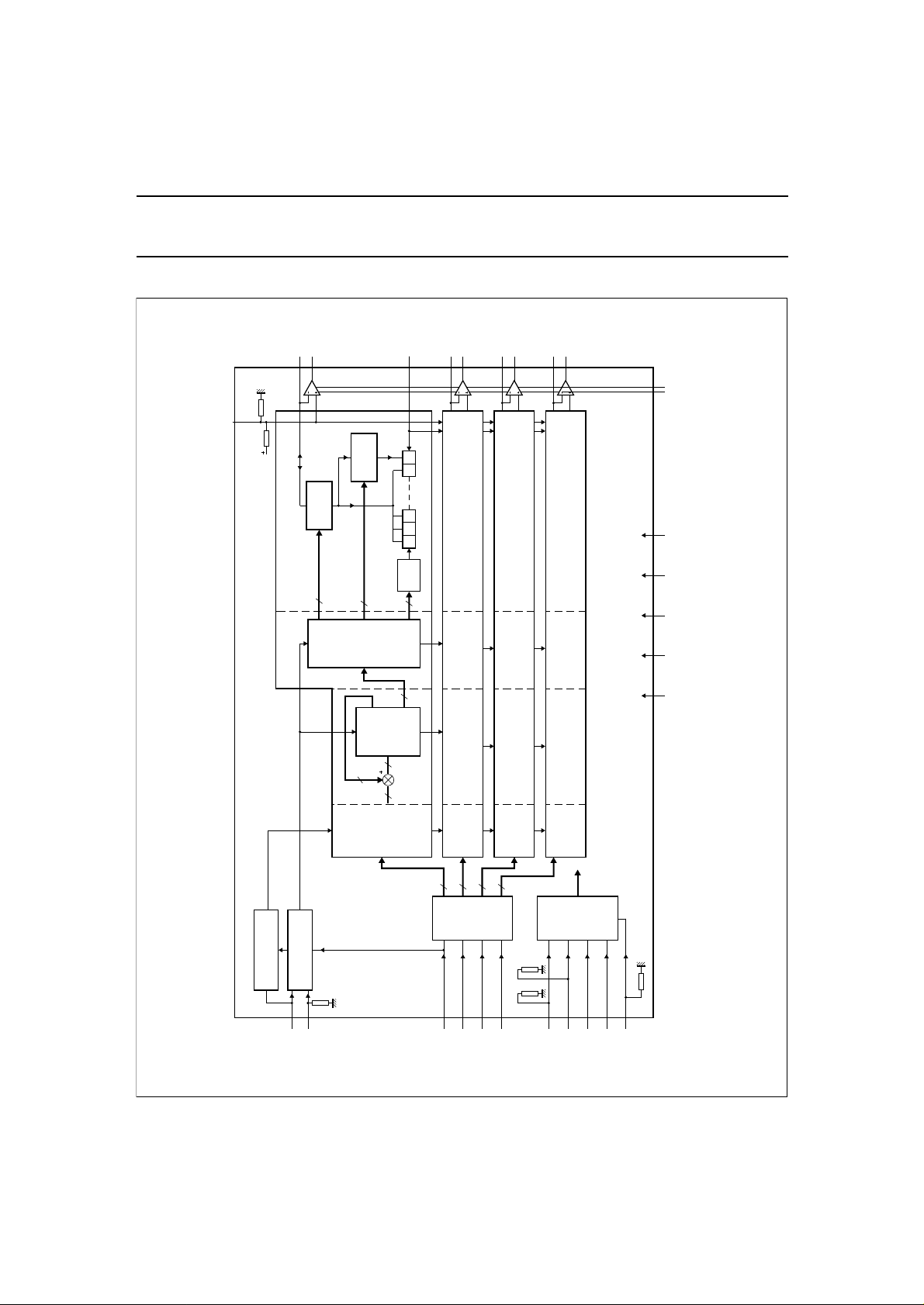
Fig.1 Block diagram.
Quadruple filter DAC TDA1314T
BLOCK DIAGRAM
August 1994 3

Philips Semiconductors Product specification
Quadruple filter DAC TDA1314T
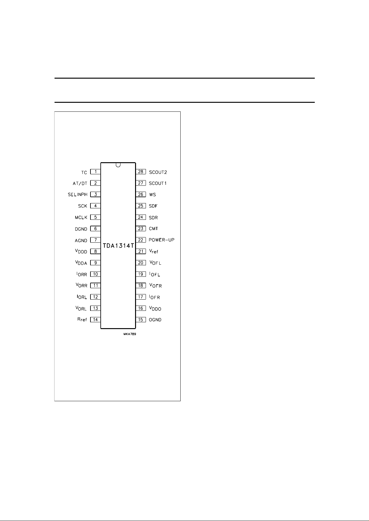
PINNING
SYMBOL PIN DESCRIPTION
TC 1 test control signal input (test/operational)
AT/DT 2 analog test/digital test select input
SELINPH 3 select in-phase 4fas mode/scan input signal 1 in test mode
SCK 4 serial clock input; I2S-bus
MCLK 5 master clock input; fi= N × 4fas (45 ≤ N ≤ 128)
DGND 6 digital ground
AGND 7 analog ground
V
DDD
V
DDA
I
ORR
V
ORR
I
ORL
V
ORL
R
ref
OGND 15 operational amplifier ground
V
DDO
I
OFR
V
OFR
I
OFL
V
OFL
V
ref
POWER-UP 22 analog mute input for all DACs
CMT 23 current mirror input test signal
SDR 24 serial data input for rear DACs (I2S-bus); scan input signal 2 in test mode
SDF 25 serial data input for front DACs (I2S-bus)
WS 26 word select input (I2S-bus)
SCOUT1 27 scan output signal 1 in test mode; 4fas signal
SCOUT2 28 scan output signal 2 in test mode; PLL lock indicator
8 digital supply voltage
9 analog supply voltage
10 DAC output current; rear right
11 DAC output voltage; rear right
12 DAC output current; rear left
13 DAC output voltage; rear left
14 resistor reference input for DACs current
16 operational amplifier supply
17 DAC output current; front right
18 DAC output voltage; front right
19 DAC output current; front left
20 DAC output voltage; front left
21 reference voltage input (1⁄2 operational amplifier supply voltage)
August 1994 4
Philips Semiconductors Product specification
Fig.2 Pin configuration.
Quadruple filter DAC TDA1314T
FUNCTIONAL DESCRIPTION
I2S-bus interface
The word select input (pin 26) is connected to the word
select line of the I2S-bus interface. This interface has
a standard I2S-bus specification as described in the
Philips
“I2S-bus specification”
9398 332 10011). Figure 4 shows an excerpt of the Philips
I2S-bus specification interface report with respect to the
general timing and format of the I2S-bus. WS logic 0
means left channel word, logic 1 means right
channel word.
The serial clock input (pin 4) must be in accordance with
the I2S-bus specification, i.e. a continuous clock.
Serial data front (SDF, pin 25) and serial data rear (SDR,
pin 24) are the I2S-bus serial data lines to be processed in
the DACs for the loudspeakers of the car (see Fig.2, blocks
DACFL and DACFR for the front loudspeakers and blocks
DACRL and DACRR for the right loudspeakers). FL stands
for Front Left, FR for Front Right, RL for Rear Left and RR
for Rear Right. In order to utilize the capabilities of this IC
fully, the data word length should be 18 bits. Signals
derived from this block are 4 × 18-bit parallel data words
which are applied to the 4fs up-sample filters.
(ordering number
August 1994 5
4ASF generator
YNTHESIZER
S
SELINPH (pin 3) and WS (pin 26) are the data inputs for
this block which generates the FASFDAC, this being the
4fas signal (at 4 times the audio sample frequency), which
is used to latch the data words to the DACs and as a
reference to the clock generator block for the up-sample
filters. It consists of a digital PLL operating at the master
clock signal MCLK (pin 5). In normal mode (i.e. in the
event that the MCLK signal on pin 5 is a jitter free clock,
with a frequency of integer multiples between 45 and 128,
of 4 times the frequency of the WS signal) this block is able
to generate a jitter free FASFDAC signal for optimum
performance of the DAC. This mode is called the free
running mode.
If, in some applications, there is considerable jitter on the
MCLK while WS is more stable (less jitter), the
phase-locked mode should be selected. This mode is
normally not used and is not recommended.

Philips Semiconductors Product specification
Quadruple filter DAC TDA1314T
UP-SAMPLE GENERATOR
This block generates the clocks for the up-sample
filters.The external pinning of the 4fas generator block is:
• MCLK (see Fig.4), which is a jitter free (maximum 30 ns
jitter) external clock at any multiple integer from
45 to 128 times 4fas (4 times the frequency of WS) of the
I2S-bus input, thus for a sample frequency of 38 kHz this
clock frequency will range from 6.840 MHz to
19.456 MHz in multiples of 152 kHz.
• The select in-phase (SELINPH) or free running mode of
the synthesizer 45 to 128. In the normal application the
free-running mode is used and this pin is not connected
(this pin is pulled down by an internal resistor). The
phase-locked mode can be selected by hard-wiring this
pin to V
(pin 8). However, this mode is
DDD
not recommended.
Test interface
This block controls the circuit in the test mode, which can
be either an analog or digital test mode. Test pins TC
(pin 1), AT/DT (pin 2), CMT (pin 23), SCOUT1 (pin 27)
and SCOUT2 (pin 28) are not connected in Fig.6.
Up-sample filter and noise shaper
The signal flow applied to the up-sample filter and noise
shaper blocks is the 4 × 18-bit parallel data words in two's
complement format from the I
2
S-bus interface at the audio
sampling frequency. The signal flow from these blocks is
the 4 × 15-bit parallel data words in two's complement
format at a frequency of 4fas. Each of the four digital filters
is a four times up-sampling filter. This up-sampling filter is
an elliptic filter of 8th order.
The filters produce an attenuation of 29 dB (min) for
signals outside the audio band. The noise shaper operates
at 4fas and reduces the word length from 22 bits to 15 bits
which is the word length of the DAC.
DAC input signals
The following signals are input to the DAC blocks FL, FR,
RL and RR:
• DATA WORD (bits 10 to 14). These 5 bits are used to
control, via a thermometer decoder, the current of the
32 coarse current sources of the analog DAC part. The
value of this data word determines the total coarse
current flowing to the DAC current output. The value of
the current of each coarse current source is determined
by the following:
; this is the current reference input at pin 14 and is at
R
ref
the same voltage level as V
. A resistor connected to
ref
OGND results in a current. This being the reference
current of the coarse current sources and subsequently
of the DAC in total.
• DATA WORD (bits 1 to 9). A current from one of the
coarse current sources is fed into a 512 transistor
matrix. The value of the DATA WORD (bits 1 to 9)
determines which part of one coarse current flows to the
DAC current output.
• DATA WORD (bit 15). This data word MSB controls the
direction of the flow of the DAC output current by
switching the current direction switch.
• V
. Voltage reference pin internally connected to a
ref
resistor divider to obtain half of the power supply
voltage. This voltage is buffered and used as reference
voltage input for the operational amplifiers and as a
reference voltage in the DAC.
• POWER-UP. The analog signal on this pin controls the
current biasing circuit of the DACs. This pin is connected
internally via a high value resistor to V
. Together with
DDA
an external capacitor a soft switch-on of the DAC output
currents is obtained. This pin can also be used as the
analog mute input for all DAC output currents by pulling
it to ground.
August 1994 6
 Loading...