

Philips TDA1311AT, TDA1311A Datasheet

INTEGRATED CIRCUITS
DATA SH EET
TDA1311A
Stereo Continuous Calibration DAC
(CC-DAC)
Preliminary specification
Supersedes data of July 1993
File under Integrated Circuits, IC01
1995 Dec 18
Philips Semiconductors Preliminary specification
Stereo Continuous Calibration DAC
(CC-DAC)
FEATURES
• Voltage output
• Space saving packages SO8 or DIP8
• Low power consumption
• Wide dynamic range (16-bit resolution)
• Continuous Calibration (CC) concept
• Easy application:
– single 4 to 5.5 V rail supply
– output current and bias current are proportional to the
supply voltage
– integrated current-to-voltage converter
• Fast settling time permits 2, 4 and 8 × oversampling
(serial input) or double-speed operation at
4 × oversampling
• Internal bias current ensures maximum dynamic range
• Wide operating temperature range (−40 °C to +85 °C)
• Compatible with most current Japanese input formats:
time multiplexed, two's complement, TTL
• No zero-crossing distortion
• Cost efficient.
TDA1311A
GENERAL DESCRIPTION
The TDA1311A; AT is a voltage-driven digital-to-analog
converter and is new generation of DAC devices which
embodies the innovative technique of Continuous
Calibration (CC). The largest bit-currents are repeatedly
generated by one single current reference source. This
duplication is based upon an internal charge storage
principle which has an accuracy insensitive to ageing,
temperature matching and process variations.
The TDA1311A; AT is fabricated in a 1.0 µm CMOS
process and features an extremely low-power dissipation,
small package size and easy application. Furthermore, the
accuracy of the intrinsic high coarse-current combined
with the implemented symmetrical offset decoding method
preclude zero-crossing distortion and ensures high quality
audio reproduction. Therefore, the CC-DAC is eminently
suitable for use in (portable) digital audio equipment.
ORDERING INFORMATION
TYPE
NUMBER
TDA1311A DIP8 plastic dual in-line package; 8 leads (300 mil) SOT97-1
TDA1311AT SO8 plastic small outline package; 8 leads; body width 3.9 mm SOT96-1
NAME DESCRIPTION VERSION
PACKAGE
1995 Dec 18 2
Philips Semiconductors Preliminary specification
Stereo Continuous Calibration DAC
TDA1311A
(CC-DAC)
QUICK REFERENCE DATA
SYMBOL PARAMETER CONDITIONS MIN. TYP. MAX. UNIT
V
DD
I
DD
V
FS
(THD+N)/S total harmonic distortion
S/N signal-to-noise ratio at
t
cs
BR input bit rate at data input −− 18.4 Mbits/s
f
BCK
TC
FS
T
amb
P
tot
supply voltage 4 5 5.5 V
supply current VDD= 5 V at code 0000H − 3.4 6.0 mA
full scale output voltage VDD= 5 V 1.8 2.0 2.2 V
at 0 dB signal level −−68 −63 dB
plus noise
− 0.04 0.07 %
at −60 dB signal level −−30 −24 dB
− 36%
at −60 dB signal level;
A-weighted
−−33 − dB
− 2 − %
A-weighted at code 0000H 86 92 − dB
bipolar zero
current settling time to ±1
− 0.2 −µs
LSB
clock frequency at clock
−− 18.4 MHz
input
full scale temperature
−±400 − ppm
coefficient at analog outputs
(IOL; IOR)
operating ambient
−40 − +85 °C
temperature
total power dissipation VDD= 5 V at code 0000H − 17 30 mW
1995 Dec 18 3
Philips Semiconductors Preliminary specification
Stereo Continuous Calibration DAC
(CC-DAC)
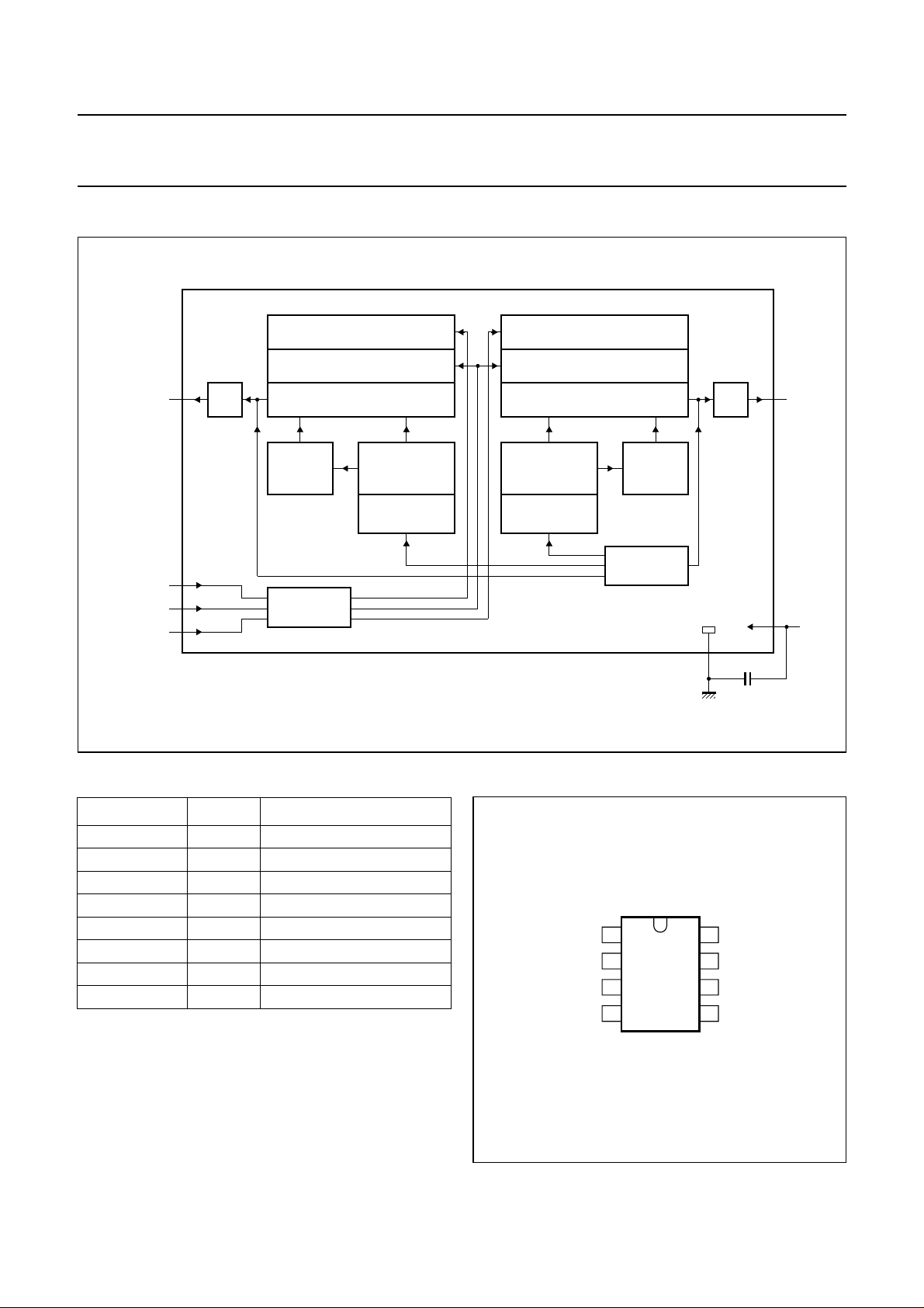
BLOCK DIAGRAM
handbook, full pagewidth
LEFT INPUT REGISTER
LEFT OUTPUT REGISTER
6
V
OL
BCK
WS
DATA
I/V
I
OL
1
2
3
LEFT BIT SWITCHES
11-BIT
PASSIVE
DIVIDER
CONTROL
AND TIMING
32 (5-BIT)
CALIBRATED
CURRENT
SOURCES
1 CALIBRATED
SPARE SOURCE
RIGHT INPUT REGISTER
RIGHT OUTPUT REGISTER
RIGHT BIT SWITCHES
32 (5-BIT)
CALIBRATED
CURRENT
SOURCES
1 CALIBRATED
SPARE SOURCE
REFERENCE
TDA1311A
TDA1311AT
MBG858
11-BIT
PASSIVE
DIVIDER
SOURCE
GND
TDA1311A
8
I/V
I
OR
5
4
C2
100 nF
V
OR
V
DD
PINNING
SYMBOL PIN DESCRIPTION
BCK 1 bit clock input
WS 2 word select input
DATA 3 data input
GND 4 ground
V
DD
V
OL
n.c.
V
OR
5 supply voltage
6 left channel output
not connected
7
8 right channel output
Fig.1 Block diagram.
handbook, halfpage
1
BCK
WS
2
TDA1311A
DATA
GND
TDA1311AT
3
4
MBG859
Fig.2 Pin configuration.
V
8
OR
n.c.
7
V
6
OL
V
5
DD
1995 Dec 18 4
Philips Semiconductors Preliminary specification
Stereo Continuous Calibration DAC
(CC-DAC)
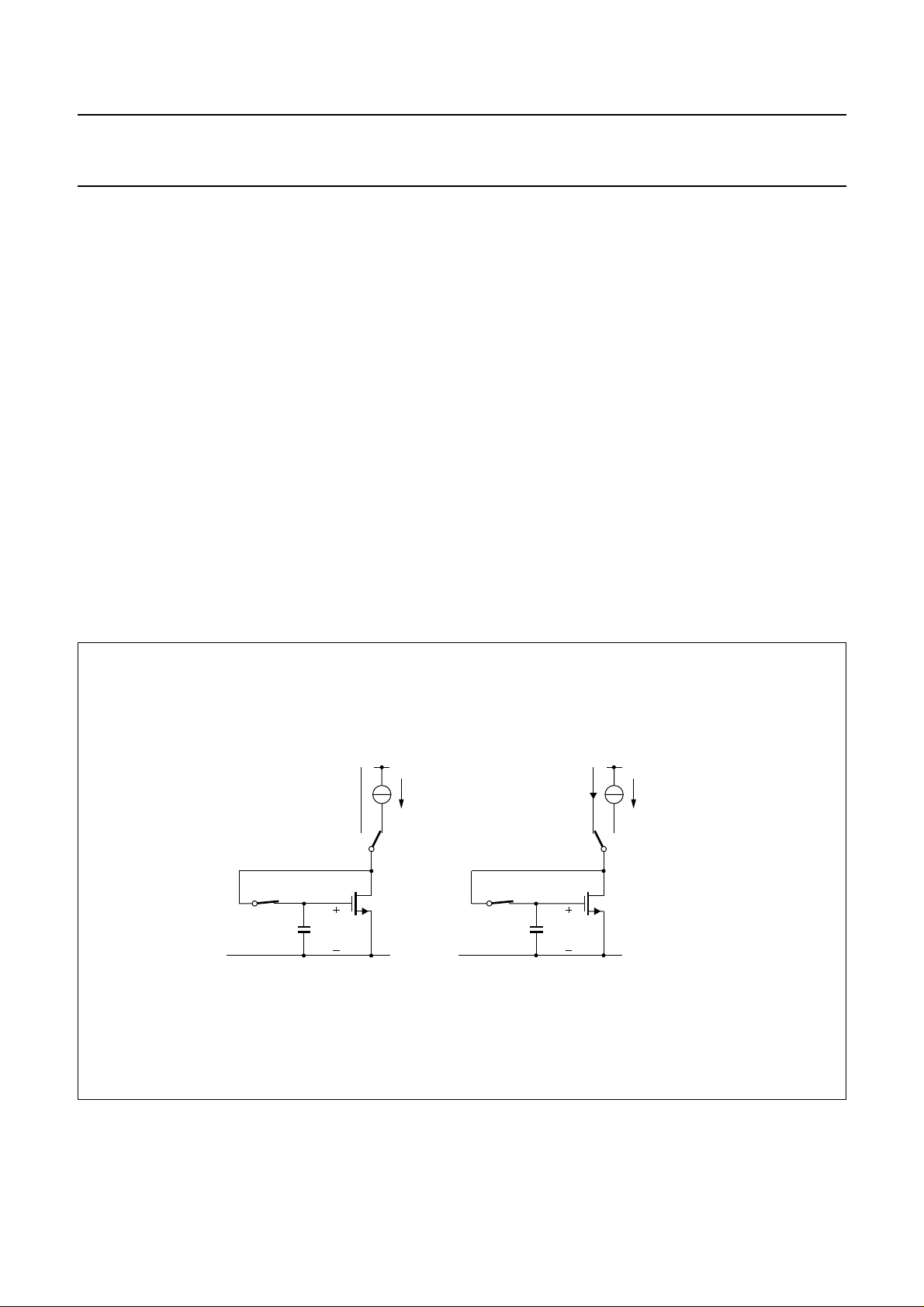
FUNCTIONAL DESCRIPTION
The basic operation of the continuous calibration DAC is
illustrated in Fig.3. The figure shows the calibration and
operation cycle. During calibration of the MOS current
source (see Fig.3a) transistor M1 is connected as a diode
by applying a reference current. The voltage Vgs on the
intrinsic gate-source capacitance Cgs of M1 is then
determined by the transistor characteristics. After
calibration of the drain current to the reference value I
the switch S1 is opened and S2 is switched to the other
position (see Fig.3b). The gate-to-source voltage Vgs of
M1 is not changed because the charge on Cgs is
preserved. Therefore, the drain current of M1 will still be
equal to I
and this exact duplicate of I
REF
REF
is now
available at the OUT terminal.
The 32 current sources and the spare current source of the
TDA1311A; AT are continuously calibrated (see Fig.1).
The spare current source is included to allow continuous
converter operation. The output of one calibrated source is
connected to an 11-bit binary current divider consisting of
2048 transistors.
REF
TDA1311A
A symmetrical offset decoding principle is incorporated
that arranges the bit switching in such a way that the
zero-crossing is performed only by switching the LSB
currents.
The TDA1311A; AT (CC-DAC) accepts serial input data
formats of 16-bit word length. Left and right data words are
time multiplexed. The most significant bit (bit 1) must
always be first. The input data format is shown in Figs 4
and 5.
,
With a HIGH level on the word select input (WS), data is
placed in the left input register and with a LOW level on the
WS input, data is placed in the right input register (see
Fig.1). The data in the input registers are simultaneously
latched in the output registers which control the bit
switches.
An internal offset voltage V
output voltage VFS; VOS and VFS are proportional to VDD:
V
DD1/VDD2=VFS1/VFS2=VOS1/VOS2
is added to the full scale
OS
.
handbook, full pagewidth
(a) =calibration.
(b) =operation.
S1
C
gs
out
I
ref
S2
M1
V
gs
(a) (b)
Fig.3 Calibration principle.
1995 Dec 18 5
S1
out
I
ref
C
gs
V
gs
M1
S2
I
ref
MBG860
Philips Semiconductors Preliminary specification
Stereo Continuous Calibration DAC
TDA1311A
(CC-DAC)
LIMITING VALUES
In accordance with the Absolute Maximum Rating System (IEC 134).
SYMBOL PARAMETER CONDITIONS MIN. MAX. UNIT
V
DD
T
stg
T
XTAL
T
amb
V
es
Note
1. Human body model: C = 100 pF, R = 1500 Ω, 3 pulses positive and 3 pulses negative.
2. Machine model: C = 200 pF, L = 0.5 µH, R = 10 Ω, 3 pulses positive and 3 pulses negative.
THERMAL RESISTANCE
SYMBOL PARAMETER VALUE UNIT
R
th j-a
supply voltage − 6.0 V
storage temperature −55 +150 °C
maximum crystal temperature − +150 °C
operating ambient temperature −40 +85 °C
electrostatic handling note 1 −2000 +2000 V
note 2 −200 +200 V
thermal resistance from junction to ambient in free air
DIL8 100 K/W
SO8 210 K/W
QUALITY SPECIFICATION
In accordance with SNW-FQ-0611.
CHARACTERISTICS
V
DD
=5V; T
=25°C; measured in Fig.1; unless otherwise specified.
amb
SYMBOL PARAMETER CONDITIONS MIN. TYP. MAX. UNIT
Supply
V
DD
I
DD
supply voltage 4.0 5.0 5.5 V
supply current at code 0000H − 3.4 6.0 mA
Digital inputs; pins WS, BCK and DATA
|I
| input leakage current LOW VI= 0.8 V −− 10 µA
IL
| input leakage current HIGH VI= 2.4 V −− 10 µA
|I
IH
f
BCK
clock frequency −− 18.4 MHz
BR bit rate data input −− 18.4 Mbits/s
f
WS
word select input frequency −− 384 kHz
1995 Dec 18 6
 Loading...