

Philips TDA1307 Datasheet
INTEGRATED CIRCUITS
DATA SH EET
TDA1307
High-performance bitstream digital
filter
Preliminary specification
Supersedes data of July 1993
File under Integrated Circuits, IC01
1996 Jan 08
Philips Semiconductors Preliminary specification
High-performance bitstream digital filter TDA1307
FEATURES
• Multiple format inputs: I2S, Sony 16, 18 and 20-bit
• 8-sample interpolation error concealment
• Digital mute, attenuation −12 dB
• Digital audio output function (biphase-mark encoded)
according to IEC 958
• Digital silence detection (output)
• Digital de-emphasis (selectable, FS-programmable)
• 8 × oversampling finite impulse response (FIR) filter
• DC-cancelling filter (selectable)
• Peak detection (continuous) and read-out to
microprocessor
• Fade function: sophisticated volume control
• Selectable 3rd/4th order noise shaping
• Selectable dither generation and automatic scaling
• Dedicated TDA1547 1-bit output
• Differential mode bitstream: complementary data
outputs available
• Simple 3-line serial microprocessor command interface
• Flexible system clock oscillator circuitry
• Power-on reset
• Standby function
• SDIP42 package.
QUICK REFERENCE DATA
Voltages are referenced to V
(ground = 0 V); all VSS and all VDD connections should be connected externally to the
SS
same supply.
SYMBOL PARAMETER CONDITIONS MIN. TYP. MAX. UNIT
V
DDC1,2,3
supply voltage
4.5 5.0 5.5 V
(pins 21, 41 and 8)
V
DDOSC
V
DDAR
V
DDAL
I
DDC1,2,3
supply voltage (pin 24) 4.5 5.0 5.5 V
supply voltage (pin 32) 4.5 5.0 5.5 V
supply voltage (pin 29) 4.5 5.0 5.5 V
supply current
VDD=5V − 75 − mA
(pins 21, 41 and 8)
I
DDOSC
I
DDAR
I
DDAL
f
XTAL
T
amb
P
tot
supply current (pin 24) VDD=5V − 2 − mA
supply current (pin 32) VDD=5V − 2 − mA
supply current (pin 29) VDD=5V − 1 − mA
oscillator clock frequency − 33.8688 − MHz
operating ambient temperature −20 − +70 °C
total power consumption − 400 − mW
ORDERING INFORMATION
PACKAGE
TYPE NUMBER
NAME DESCRIPTION VERSION
TDA1307 SDIP42 plastic shrink dual in-line package; 42 leads (600 mil) SOT270-1
1996 Jan 08 2

Philips Semiconductors Preliminary specification
High-performance bitstream digital filter TDA1307
GENERAL DESCRIPTION
The TDA1307 is an advanced oversampling digital filter
employing bitstream conversion technology, which has
been designed for use in premium performance digital
audio applications. Audio data is input to the TDA1307
through its multiple-format interface. Any of the four
formats (I2S, Sony 16, 18 or 20-bit) are acceptable. By
using a highly accurate audio data processing structure,
including 8 times oversampling digital filtering and up to
4th order noise shaping, a high quality bitstream is
produced which, when used in the recommended
combination with the TDA1547 bitstream DAC, provides
the optimum in dynamic range and signal-to-noise
performance. With the TDA1307, a high degree of
versatility is achieved by a multitude of functional features
and their easy accessibility; error concealment functions,
f
handbook, full pagewidth
20-bit f
s
= 768f
system
TDA1307 TDA1547
s
1-bit, 192f
s
audio peak data information and an advanced patented
digital fade function are accessible through a simple
microprocessor command interface, which also provides
access to various integrated system settings
and functions.
TDA1307 plus TDA1547 high-performance bitstream
digital filter plus DAC combination:
For many features:
• Highly accessible structure
• Intelligent audio data processing.
For optimum performance:
• 4th order noise shaping
• Improvement dynamic range (113 dB)
• Improvement signal-to-noise (115 dB).
L
R
8 × oversampling FIR
filter, 20-bit
24 × upsampling
3rd or 4th order noise shaping,
1-bit end quantization
1-bit high-performance
digital-to-analog
converter
Fig.1 High performance bitstream reconstruction system.
3rd order analog
postfilter, fo = 55 kHz
Butterworth response
MGB983
1996 Jan 08 3

Philips Semiconductors Preliminary specification
High-performance bitstream digital filter TDA1307
BLOCK DIAGRAM
handbook, full pagewidth
DSR
DSL
TEST1
TEST2
RAB
POR
V
DDC3
V
DDC1
V
DDOSC
V
DDAL
V
DDAR
V
DDC2
1fs AUDIO DATA INPUTS
WS SCK
1234
MULTIPLE FORMAT
INPUT INTERFACE
ERROR CONCEALMENT,
INTERPOLATION, MUTING
12
11
36
37
38
DA
39
CL
42
20
8
21
24
29
32
41
MICRO–
PROCESSOR
INTERFACE
DIGITAL SILENCE DETECTION
DE–EMPHASIS FILTER
FIR HALFBAND FILTER
STAGE 1: 1fs to 2f
DC–CANCELLING FILTER
PEAK DETECTION
FADE FUNCTION
VOLUME CONTROL
FIR HALFBAND FILTER
STAGE 2: 2fs to 4f
FIR HALFBAND FILTER
STAGE 3: 4fs to 8f
DITHER AND SCALING
SD EFAB
s
s
s
DIGITAL
OUTPUT
TDA1307
OSCILLATOR
CLOCK
GENERATION
DISTRIBUTION
CRYSTAL
AND
19
RESYNC
10
DOBM
13
DSTB
5
SBCL
6
SBDA
25
V
SSOSC
22
XTAL1
23
XTAL2
15
CMIC
7
CDEC
14
CLC1
17
CLC2
18
CDCC
9
V
SSC2
16
V
SSC3
30
V
SSAL
31
V
SSAR
40
V
SSC1
3rd/4th ORDER
NOISE SHAPER
27 28 35 34 33 26
DOL NDOL CDAC NDOR
BITSTREAM DATA OUTPUTS
Fig.2 Block diagram.
1996 Jan 08 4
DOR MODE
MGB989
Philips Semiconductors Preliminary specification
High-performance bitstream digital filter TDA1307
PINNING
SYMBOL PIN TYPE, I/O DESCRIPTION
WS 1 I word select input to data interface
SCK 2 I clock input to data interface
SD 3 I data input to interface
EFAB 4 I
SBCL 5 I subcode clock: a 10-bit burst clock (typ. 2.8224 MHz) input which synchronizes
SBDA 6 I subcode data: a 10-bit burst of data, including flags and sync bits, serially input
CDEC 7 O decoder clock output: frequency division programmable by means of
V
V
DDC3
SSC2
8 positive supply 3
9 ground 2
DOBM 10 O digital audio output: this output contains digital audio samples which have
DSL 11 O digital silence detected (active LOW) on left channel
DSR 12 O digital silence detected (active LOW) on right channel
DSTB 13 I
CLC1 14 I application mode programming pin for CDEC (pin 7) frequency division
CMIC 15 O clock output, provided to be used as running clock by microprocessor
V
SSC3
16 ground 3
CLC2 17 I application mode programming pin for CDEC (pin 7) frequency division
CDCC 18 I master / slave mode selection pin
RESYNC 19 O resynchronization: out-of-lock indication from data input section (active HIGH)
POR 20 I
V
DDC1
21 supply voltage 1
XTAL1 22 I crystal oscillator terminal: local crystal oscillator sense forced input in slave mode
XTAL2 23 O crystal oscillator output: drive output to crystal
V
DDOSC
V
SSOSC
24 positive supply connection to crystal oscillator circuitry
25 ground connection to crystal oscillator circuitry
MODE 26 I
DOL 27 O data output left channel to bitstream DAC TDA1547
NDOL 28 O complementary data output left channel to TDA1547 in double differential mode
V
DDAL
V
SSAL
V
SSAR
V
DDAR
29 positive supply connection to output data driving circuitry, left channel
30 ground connection to output data driving circuitry, left channel
31 ground connection to output data driving circuitry, right channel
32 positive supply connection to output data driving circuitry, right channel
DOR 33 O data output right channel to TDA1547
(1)
(2)
(2)
(2)
error flag (active HIGH): input from decoder chip indicating unreliable data
the subcode data
once per frame, clocked by burst clock input SBCL
pins 14 (CLC1) and 17 (CLC2) to output 192, 256, 384 or 768 times f
s
received interpolation, attenuation and muting plus subcode data;
transmission is in biphase-mark code
DOBM standby mode enforce pin (active HIGH)
(in master mode only), output 96f
s
power-on reset (active LOW)
evaluation mode programming pin (active LOW); in normal operation, this pin
should be left open-circuit or connected to the positive supply
1996 Jan 08 5

Philips Semiconductors Preliminary specification
High-performance bitstream digital filter TDA1307
SYMBOL PIN TYPE, I/O DESCRIPTION
NDOR 34 O complementary data output right channel to TDA1547 in double differential mode
CDAC 35 O clock output to bitstream DAC TDA1547
TEST1 36 I
TEST2 37 I
DA 38 I/O
CL 39 I
V
SSC1
V
DDC2
RAB 42 I
Notes
1. These pins are configured as internal pull-down.
2. These pins are configured as internal pull-up.
(1)
(1)
(2)
test mode input; in normal operation this pin should be connected to ground
test mode input; in normal operation this pin should be connected to ground
bidirectional data line intended for control data from the microprocessor and peak
data from the TDA1307
(2)
clock input, to be generated by the microprocessor
40 ground 1
41 supply voltage 2
(2)
command / peak data request line
handbook, halfpage
WS
SCK
SD
EFAB
SBCL
SBDA
CDEC
V
DDC3
V
SSC2
DOBM
DSL
DSR
DSTB
CLC1
CMIC
V
SSC3
CLC2
CDCC
RESYNC
POR
V
DDC1
1
2
3
4
5
6
7
8
9
10
11
12
13
14
15
16
17
18
19
20
TDA1307
MGB980
42
RAB
41
V
DDC2
40
V
SSC1
39
CL
38
DA
37
TEST2
36
TEST1
35
CDAC
34
NDOR
33
DOR
32
V
DDAR
31
V
SSAR
30
V
SSAL
29
V
DDAL
28
NDOL
27
DOL
26
MODE
25
V
SSOSC
24
V
DDOSC
23
XTAL2
2221
XTAL1
Fig.3 Pin configuration.
1996 Jan 08 6
Philips Semiconductors Preliminary specification
High-performance bitstream digital filter TDA1307
FUNCTIONAL DESCRIPTION
In the block diagram, Fig.1, a general subdivision into
three main functional sections is illustrated. The actual
signal processing takes place in the central sequence of
blocks, a representation of the audio data path from top to
bottom. The two blocks named “Microprocessor Interface”
and “Clock Generation and Distribution” fulfil a general
auxiliary function to the audio data processing path. The
Microprocessor Interface provides access to all the blocks
in the audio path that require or allow for configuration or
selection, and manipulates data read-out from the Peak
Detection block, all via a simple three-line interface. The
Clock Generation and Distribution section, driven either by
its integrated oscillator circuit with external crystal or by an
externally provided master clock, provides the data
processing blocks with timebases, manages the system
mode dependent frequency settings, and conveniently
generates clocks for external use by the system decoder
IC and microprocessor. Following are detailed
explanations of the functions of each block in the audio
data processing path and their setting options manipulated
by the microprocessor interface, the use of the
microprocessor interface, and the functions of the clock
section with its various system settings.
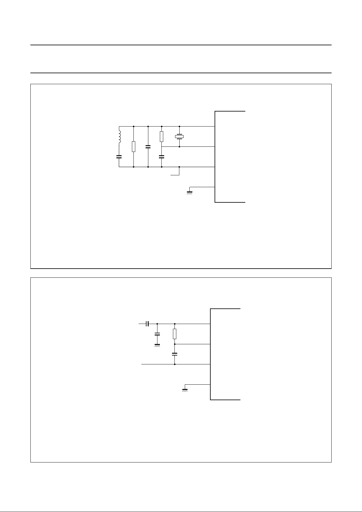
Clock generation and distribution
The clock generation section of the TDA1307 is designed
to accommodate two main modes. The master mode, in
which the TDA1307 is the master in the digital audio
system, and for which the clock is generated by connecting
a crystal of 768f
(33.8688 MHz) to the crystal oscillator
s
pins XTAL1 (pin 22) and XTAL2 (pin 23); and the slave
mode, in which the TDA1307 is supplied a clock by the IC
in the system that acts as the master (e.g. the digital audio
interface receiver). In this event a clock signal frequency of
256fs is input to pin XTAL1. Master or slave mode is
programmed by means of pin CDCC (pin 18) logic 1 for
master and logic 0 for slave mode. The circuit diagram of
Fig.4 shows the typical connection of the external
oscillator circuitry and crystal resonator for master mode
operation. Note that the positive supply V
DDOSC
is the
reference to the oscillator circuitry. The LC network is used
for suppression of the fundamental frequency component
of the overtone crystal. Figure 5 shows how to connect for
slave mode operation. A clock frequency of typical 256f
and levels of 0 V/+5 V is input to XTAL1 via AC coupling.
The 100 kΩ resistor and the 10 nF capacitor are required
to provide the necessary biasing for XTAL2 by filtering and
feeding back the output signal of XTAL1.
Besides generating all necessary internal clocks for the
audio data processing blocks and the clock to the DAC, the
clock generation block further provides two clocks for
external use when operating in master mode. Pin CDEC
(pin 7) is used as the running clock for the system
decoder IC, and pin CMIC (pin 15) is used as the running
clock for the system microprocessor. CMIC outputs, by a
fixed divider ratio to XTAL2, a clock signal at 96fs. For
CDEC the divider ratio is programmable by means of pins
CLC1 (pin 14) and CLC2 (pin 17). Table 1 gives the clock
divider programming relationships.
s
Table 1 Clock divider programming
CLC1 CLC2 CDEC OUTPUT FREQUENCY
0 0 256f
0 1 384f
1 0 768f
1 1 192f
1996 Jan 08 7
s
s
s
s
Philips Semiconductors Preliminary specification
High-performance bitstream digital filter TDA1307
handbook, halfpage
XTAL2
23
3.3
µH
1 nF
10
kΩ
10
pF
100
+5 V
kΩ
10
pF
33.8688
MHz
V
V
XTAL1
DDOSC
SSOSC
22
TDA1307
24
25
MGB981
Fig.4 External crystal oscillator circuit.
handbook, halfpage
fi = 256f
s
+5 V
20 pF
30
pF
100 kΩ
10 nF
XTAL2
XTAL1
V
DDOSC
V
SSOSC
23
22
TDA1307
24
25
MGB982
Fig.5 External clock input connections.
1996 Jan 08 8
Philips Semiconductors Preliminary specification
High-performance bitstream digital filter TDA1307
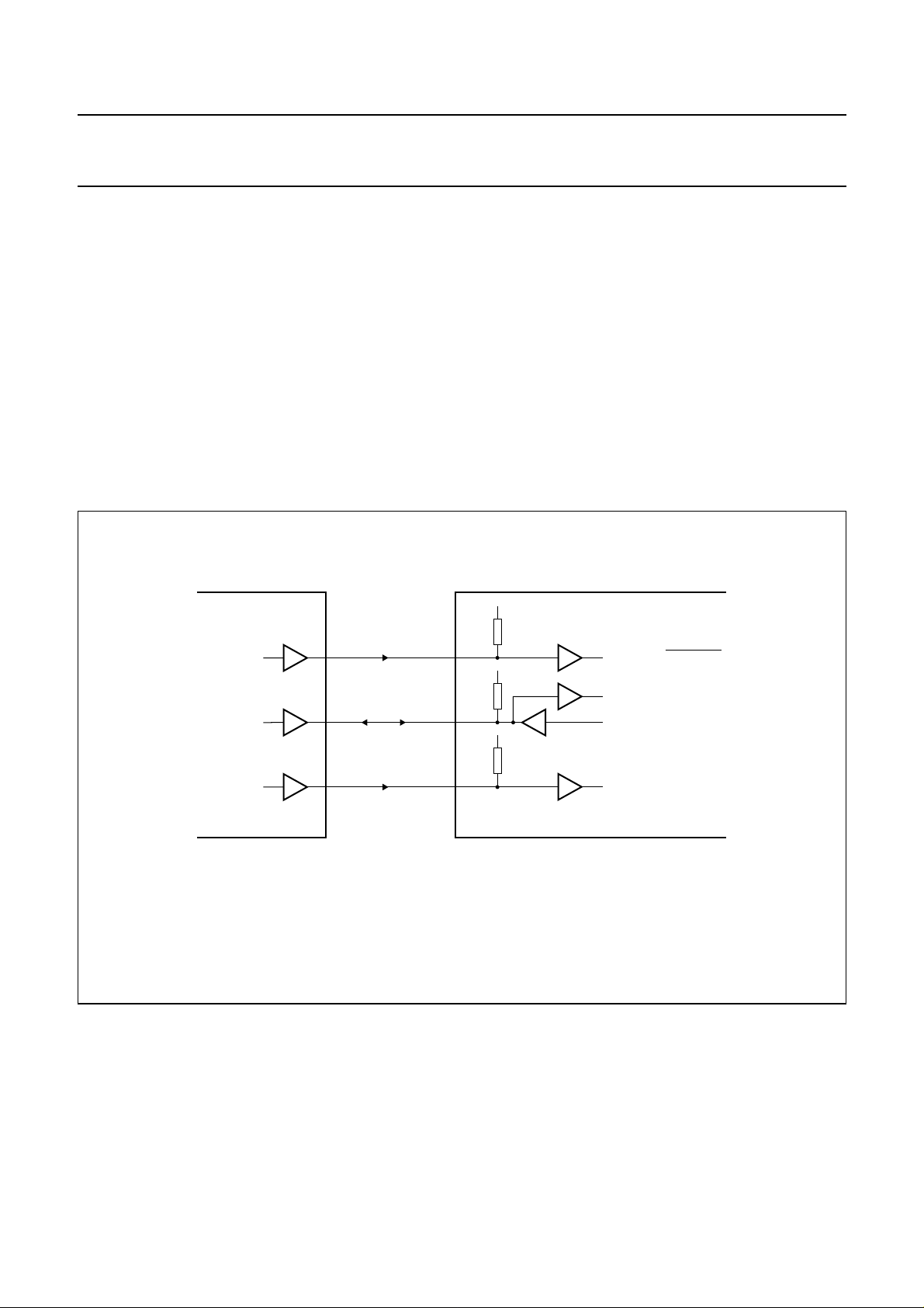
Microprocessor interface
The microprocessor interface provides access to virtually
all of the functional blocks in the audio data processing
section. Its destination is two-fold: system constants (such
as input format and sample frequency) as well as system
variables (attenuation, muting, de-emphasis, volume
control data etc.) can be ‘written to’ the respective blocks
(command mode), and continuously collected stereo peak
data ‘read from’ the peak detection block (peak request).
The system settings are stored in the TDA1307 in an
internal register file. Peak data is read from the stereo
peak value register.
handbook, full pagewidth
RAB 42
DA/ACK 38
THREE-LINE MICROPROCESSOR INTERFACE BUS
Communication is realized by a three-line bus, consisting
of the following signals (see Fig.6):
• Clock input CL (pin 39), to be generated by the
microprocessor
• Command/request input RAB (pin 42), by which either
of the two mode commands (RAB = 0) and peak request
(RAB = 1) are invoked
• Bidirectional data line DA (pin 38), which either receives
command data from the microprocessor or outputs peak
data from the peak detection block.
CL and RAB both default HIGH by internal pull-up, DATA
is 3-state (high impedance, pull-up, pull-down).
+
REQUEST/COMMAND
+
COMMAND DATA
PEAK DATA
+
CL 39
MICROPROCESSOR
Fig.6 Three-line microprocessor interface bus.
1996 Jan 08 9
CLOCK
TDA1307
MGB984

Philips Semiconductors Preliminary specification
High-performance bitstream digital filter TDA1307
INITIALIZATION OF THE BUS RECEIVER
The microprocessor interface section is initialized
automatically by the power-on reset function, POR
(pin 20). A LOW input on POR will initiate the reset
procedure, which encompasses a functional reset plus
setting of the initial states of the control words in the
command register file. A wait time of at least one audio
sample time after a LOW-to-HIGH transition of POR must
be observed before communication can successfully be
established between the TDA1307 and the
microprocessor. In addition to the POR function, a
software reset function issued from the microprocessor is
provided (see section “Organization and programming of
the internal register file”), which has the sole function of
reinstating the initial values of the microprocessor control
register. More information on initializing the TDA1307 can
be found under “Application Information”.
C
OMMAND PROTOCOL
The protocol for writing data to the TDA1307 is illustrated
in Fig.7. The command mode is invoked by forcing RAB
LOW. A unit command is given in the form of an 8-bit burst
on the DA line, clocked on the rising edge of CL.
The command consists of 4 address bits followed by
4 control data bits (both MSB first). A next command may
be immediately issued while keeping RAB forced LOW.
Only commands for which the MSB of the address bits is
LOW are accepted; of the remaining set of addresses, only
four have meaning (see section “Organization and
programming of the internal register file”). The command
input receiver is provided with a built-in protection against
erroneous command transfer due to spikes, by a 2-bit
debounce mechanism on lines DA and CL. The
waveforms on these lines are sampled by the receiver at
the internal system clock rate 256f
. A state transition on
s
DA or CL is accepted only when the new state perseveres
for two consecutive sampled waveform instants.
O
RGANIZATION AND PROGRAMMING OF THE INTERNAL
REGISTER FILE
Command data received from the microprocessor is
stored in an internal register file (see Table 2), which is
organized as a page of 10 registers, each containing a
4-bit command data word (D3 to D0). Access to the words
in the register file involves two controls: selection of the
address of a set of registers (by means of A3, A2,
A1 and A0) and setting the number of the bank in which
the desired register is located (by means of the ‘bank bits’
B0 and B1). First the desired bank is selected by
programming the command word at address 0000
(supplying the bank bits plus refreshing bits ATT and DIM).
A subsequent addressing (one of three addresses, 1H, 4H
and 6H) will yield access to the register corresponding to
the last set bank.
handbook, full pagewidth
RAB
CL
DA (TDA1307)
DA (µP)
DA
t
DRW
t
CKL
1
t
DSM
A3 A2 A1 A0 D3 D2 D1 D0
A3 A2 A1 A0 D3 D2 D1 D0
t
t
CKH
Fig.7 Microprocessor command protocol.
1996 Jan 08 10
t
DHM
8
MGB995

Philips Semiconductors Preliminary specification
High-performance bitstream digital filter TDA1307
Table 2 Microprocessor control register file
ADDRESS
A3 A2 A1 A0
BANK
B0 B1
0000X XBANK B0 BANK B1 ATT DIM 0 0 1 1
00010 1FCON DIT FSS9 FSS8 0 0 0 0
1 0 FSS7 FSS6 FSS5 FSS4 0 0 1 0
1 1 FSS3 FSS2 FSS1 FSS0 1 0 0 0
01000 1DCEN DCSH FN9 FN8 0 1 1 1
1 0 FN7 FN6 FN5 FN4 0 0 0 0
1 1 FN3 FN2 FN1 FN0 1 1 0 1
01100 1DEMC1 DEMC0 RES0 RES1 0 0 0 0
1 0 INS1 INS0 FS1 FS0 0 0 0 0
1 1 RES2 NS RST STBY 1 0 0 0
Following is a list of the programming values for the
various control words in the register file. Information on the
meaning of the different controls can be found under the
sections covering the corresponding signal processing
blocks (see sections “Multiple format input interface” to
“Third and fourth order noise shaping”).
BANK B0, BANK B1
D3 D2 D1 D0 INITIAL STATE
DIT
Dither control bit: logic 1 to activate dither addition, logic 0
deactivates.
FSS9 to FSS0
Fade function 10-bit control value to program fade speed,
in number of samples per fade step.
Programming of the bank bits is given in Table 2. The bank
bits can be changed by addressing register location 0000.
Subsequent addressing will result in access of locations
according to the last selected bank.
ATT
Attenuation control bit: logic 1 to activate −12 dB
attenuation, logic 0 to deactivate. As the attenuate control
bit shares a control word with the bank bits, ATT has to be
refreshed each time a new bank is selected.
DIM
Digital mute control bit: logic 1 to activate mute, logic 0 to
deactivate. An active digital mute will override the
attenuation function. As with ATT, DIM needs to be
refreshed with each change in bank selection.
FCON
Fade function control bit: logic 1 to activate the fade
function, logic 0 to deactivate.
DCEN
DC-filter enable bit: logic 1 enables subtraction of the
DC-level from the input signal, logic 0 disables.
DCSH
DC-filter sample or hold control bit: when DCSH = 0 the
DC-level of the input signal is continuously evaluated.
When DCSH = 1 the once acquired DC value, to be
subtracted from the input signal, is held constant.
FN9 to FN0
Fade function 10-bit control value to program volume level.
DEMC1, DEMC0
De-emphasis function enable and fs selection bits.
1996 Jan 08 11
 Loading...