

Philips TDA1306T-N1, TDA1306T-N2 Datasheet

DATA SH EET
Product specification
Supersedes data of September 1994
File under Integrated Circuits, IC01
1998 Jan 06
INTEGRATED CIRCUITS
TDA1306T
Noise shaping filter DAC

1998 Jan 06 2
Philips Semiconductors Product specification
Noise shaping filter DAC TDA1306T
FEATURES
General
• Double-speed mode
• Digital volume control
• Soft mute function
• 12 dB attenuation
• Low power dissipation
• Digital de-emphasis
• TDA1305T pin compatible.
Easy application
• Voltage output
• Only 1st-order analog post-filtering required
• Operational amplifiers and digital filter integrated
• Selectable system clock (f
sys
) 256fs or 384f
s
• I2S-bus (f
sys
= 256fs) or 16, 18 or 20 bits LSB fixed
serial input format (f
sys
= 384fs)
• Single rail supply.
High performance
• Superior signal-to-noise ratio
• Wide dynamic range
• No zero crossing distortion
• Inherently monotonic
• Continuous calibration digital-to-analog conversion
combined with noise shaping technique.
GENERAL DESCRIPTION
The TDA1306T is a dual CMOS digital-to-analog
converter with up-sampling filter and noise shaper.
The combination of oversampling up to 4f
s
, noise shaping
and continuous calibration conversion ensures that only
simple 1st-order analog post-filtering is required.
The TDA1306T supports the I2S-bus data input mode
(f
sys
= 256fs) with word lengths of up to 20 bits and the
LSB fixed serial data input format (f
sys
= 384fs) with word
lengths of 16, 18 or 20 bits. Two cascaded IIR filters
increase the sampling rate 4 times.
The DACs are of the continuous calibration type and
incorporate a special data coding. This ensures a high
signal-to-noise ratio, wide dynamic range and immunity to
process variation and component ageing.
Two on-board operational amplifiers convert the
digital-to-analog current to an output voltage.
ORDERING INFORMATION
TYPE NUMBER
PACKAGE
NAME DESCRIPTION VERSION
TDA1306T SO24 plastic small outline package; 24 leads; body width 7.5 mm. SOT137−1
1998 Jan 06 3
Philips Semiconductors Product specification
Noise shaping filter DAC TDA1306T
QUICK REFERENCE DATA
All power supply pins VDD and VSS must be connected to the same external supply unit.
SYMBOL PARAMETER CONDITIONS MIN. TYP. MAX. UNIT
Supply
V
DDD
digital supply voltage 4.5 5.0 5.5 V
V
DDA
analog supply voltage 4.5 5.0 5.5 V
V
DDO
operational amplifier
supply voltage
4.5 5.0 5.5 V
I
DDD
digital supply current V
DDD
=5V;
at code 00000H
− 58mA
I
DDA
analog supply current V
DDA
=5V;
at code 00000H
− 35mA
I
DDO
operational amplifier
supply current
V
DDO
=5V;
at code 00000H
− 24mA
Analog signals
V
FS(rms)
full-scale output voltage
(RMS value)
V
DDD=VDDA=VDDO
=5V;
RL>5kΩ
0.935 1.1 1.265 V
R
L
output load resistance 5 −−kΩ
DAC performance
(THD + N)/S total harmonic distortion
plus noise-to-signal ratio
at 0 dB signal level;
fi= 1 kHz;
−−70 − dB
− 0.032 − %
at −60 dB signal level;
fi= 1 kHz;
−−42 −32 dB
− 0.8 2.5 %
S/N signal-to-noise ratio no signal; A-weighted −−108 −96 dB
BR input bit rate at data input f
s
= 44.1 kHz;
normal speed
−−2.822 Mbits/s
f
s
= 44.1 kHz;
double speed
−−5.645 Mbits/s
f
sys
system clock frequency
(pin 12)
6.4 − 18.432 MHz
T
amb
operating ambient
temperature
−40 − +85 °C
1998 Jan 06 4
Philips Semiconductors Product specification
Noise shaping filter DAC TDA1306T
BLOCK DIAGRAM
Fig.1 Block diagram.
1998 Jan 06 5
Philips Semiconductors Product specification
Noise shaping filter DAC TDA1306T
PINNING
SYMBOL PIN DESCRIPTION
V
DDA
1 analog supply voltage (+5 V)
V
SSA
2 analog ground
TEST1 3 test input 1; pin should be connected
to ground
BCK 4 bit clock input
WS 5 word select input
DATA 6 data input
CLKS1 7 clock and format selection 1 input
CLKS2 8 clock and format selection 2 input
V
SSD
9 digital ground
V
DDD
10 digital supply voltage (+5 V)
TEST2 11 test input 2; pin should be connected
to ground
SYSCLK 12 system clock input 256fsor 384f
s
APP3 13 application mode 3 input
APPL 14 application mode selection input
APP2 15 application mode 2 input
APP1 16 application mode 1 input
APP0 17 application mode 0 input
V
OL
18 left channel output
FILTCL 19 capacitor for left channel 1st order
filter function; should be connected
between pins 19 and 18
FILTCR 20 capacitor for right channel 1st order
filter function; should be connected
between pins 20 and 21
V
OR
21 right channel output
V
ref
22 internal reference voltage for output
channels; 0.5V
DDO
(typ.)
V
SSO
23 operational amplifier ground
V
DDO
24 operational amplifier supply voltage
Fig.2 Pin configuration.
1998 Jan 06 6
Philips Semiconductors Product specification
Noise shaping filter DAC TDA1306T
FUNCTIONAL DESCRIPTION
The TDA1306T CMOS DAC incorporates an up-sampling
filter, a noise shaper, continuous calibrated current
sources and operational amplifiers.
System clock and data input format
The TDA1306T accommodates slave mode only.
Consequently, in all applications, the system devices must
provide the system clock. The system frequency is
selectable at pins CLKS1 and CLKS2 (see Table 1).
The TDA1306T supports the following data input modes:
• I
2
S-bus with data word length of up to 20 bits
(f
sys
= 256fs)
• LSB fixed serial format with data word length of 16, 18
or 20 bits (f
sys
= 384fs). As this format idles on the MSB
it is necessary to know how many bits are being
transmitted.
The input formats are illustrated in Fig.9. Left and right
data channel words are time multiplexed.
Table 1 Data input format and system clock
CLKS1 CLKS2 DATA INPUT FORMAT
SYSTEM CLOCK
NORMAL SPEED DOUBLE SPEED
00I
2
S-bus 256f
s
128f
s
0 1 LSB fixed 16 bits 384f
s
192f
s
1 0 LSB fixed 18 bits 384f
s
192f
s
1 1 LSB fixed 20 bits 384f
s
192f
s
Device operation
When the APPL pin is held HIGH and APP3 is held LOW,
pins APP0, APP1 and APP2 form a microcontroller
interface. When the APPL pin is held LOW, pins APP0,
APP1, APP2 and APP3 form a pseudo-static application
(TDA1305T pin compatible).
P
SEUDO-STATIC APPLICATION MODE (APPL = LOGIC 0)
In this mode, the device operation is controlled by
pseudo-static application pins where:
APP0 = attenuation mode control
APP1 = double-speed mode control
APP2 = mute mode control
APP3 = de-emphasis mode control.
In the pseudo-static application mode the TDA1306T is pin
compatible with the TDA1305T slave mode.
The correspondence between TDA1306T pin number,
TDA1306T pin name, TDA1305T pin mnemonic and a
description of the effects is given in Table 2.
1998 Jan 06 7
Philips Semiconductors Product specification
Noise shaping filter DAC TDA1306T
Table 2 Pseudo-static application mode
PIN
MNEMONIC
PIN NUMBER
TDA1305T
FUNCTION
VALUE DESCRIPTION
APP0 17 ATSB 0 12 dB attenuation (from full scale) activated
(only if MUSB = logic 1)
1 full scale (only if MUSB = logic 1)
APP1 16 DSMB 0 double-speed mode
1 normal-speed mode
APP2 15 MUSB 0 samples decrease to mute level
1 level according to ATSB
APP3 13 DEEM1 0 de-emphasis OFF (44.1 kHz)
1 de-emphasis ON (44.1 kHz)
MICROCONTROLLER APPLICATION MODE (APPL = LOGIC
1 AND APP3 = LOGIC 0)
In this mode, the device operation is controlled by a set of
flags in an 8-bit mode control register. The 8-bit mode
control register is written by a microcontroller interface
where:
APPL = logic 1
APP0 = Data
APP1 = Clock
APP2 = RAB
APP3 = logic 0.
The correspondence between serial-to-parallel
conversion, mode control flags and a summary of the
effect of the control flags is given in Table 3.
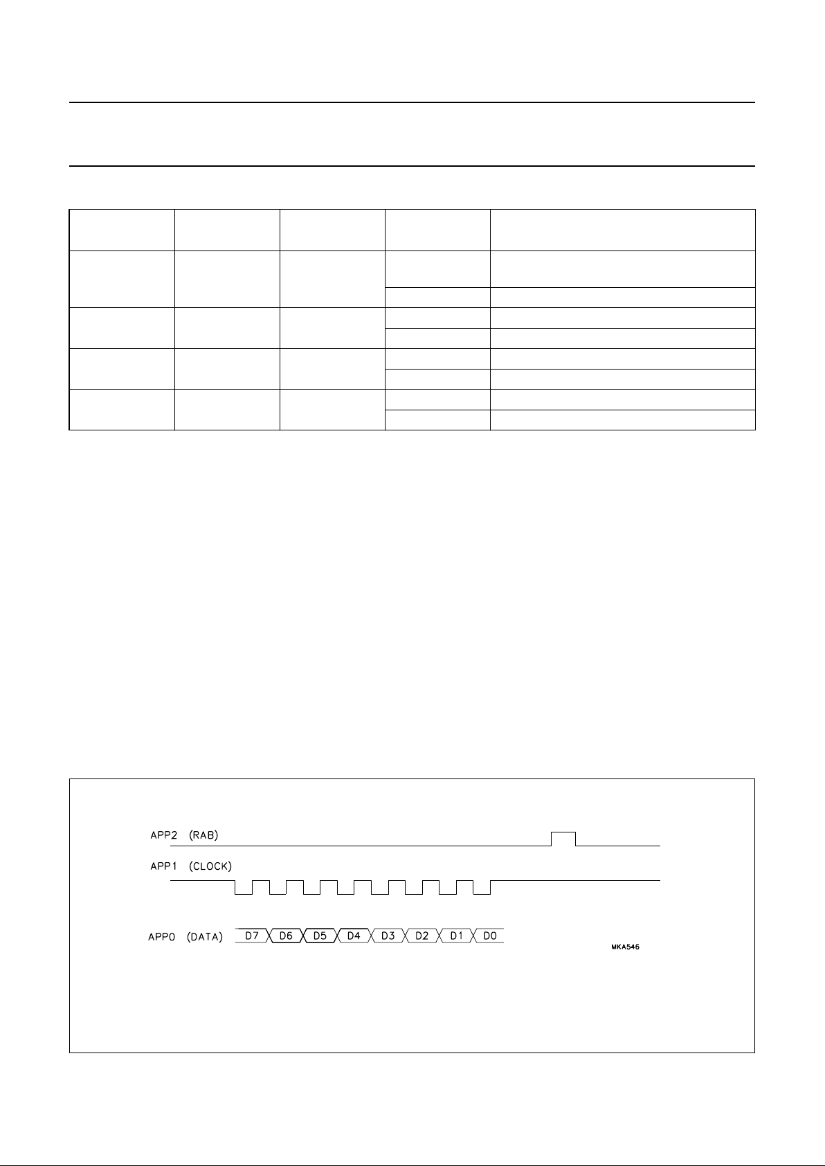
Figures 3 and 4 illustrate the mode set timing.
M
ICROCONTROLLER WRITE OPERATION SEQUENCE
The microcontroller write operation follows the following
sequence:
• APP2 is held LOW by the microcontroller
• Microcontroller data is clocked into the internal shift
register on the LOW-to-HIGH transition on pin APP1
• Data D7 to D0 is latched into the appropriate control
register on the LOW-to-HIGH transition of pin APP2
(APP1 = HIGH)
• If more data is clocked into the TDA1306T before the
LOW-to-HIGH transition on pin APP2 then only the last
8 bits are used
• If less data is clocked into the TDA1306T unpredictable
operation will result
• If the LOW-to-HIGH transition of pin APP2 occurs when
APP1 = LOW, the command will be disregarded.
Fig.3 Microcontroller timing.
1998 Jan 06 8
Philips Semiconductors Product specification
Noise shaping filter DAC TDA1306T
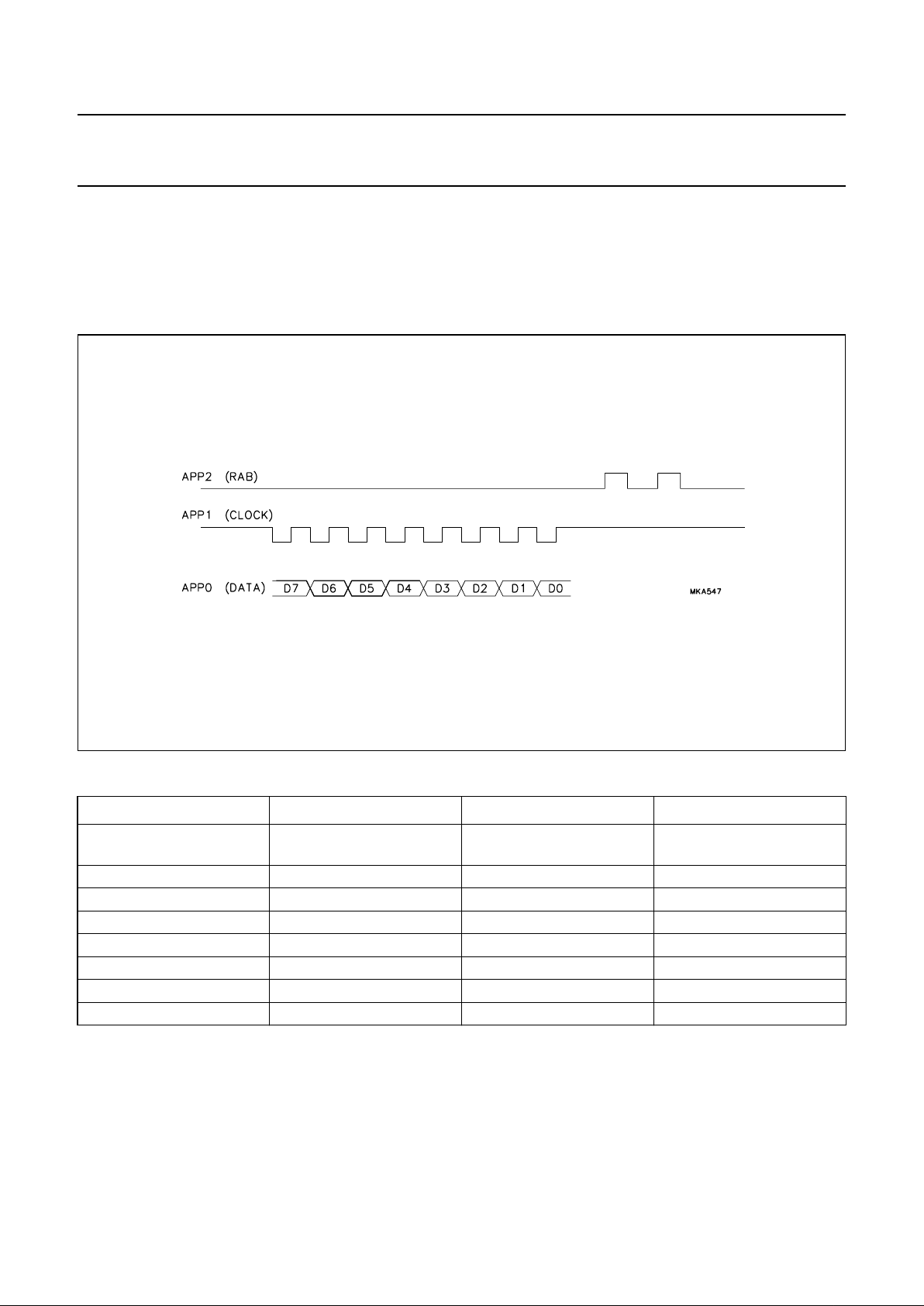
MICROCONTROLLER WRITE OPERATION SEQUENCE (REPEAT
MODE
)
The same command can be repeated several times (e.g.
for fade function) by applying APP2 pulses as shown in
Fig.4. It should be noted that APP1 must stay HIGH
between APP2 pulses. A minimum pause of 22 µs is
necessary between any two step-up or step-down
commands.
Table 3 Microcontroller mode control register
BIT POSITION FUNCTION DESCRIPTION ACTIVE LEVEL
D7 ATSB 12 dB attenuation
(from full scale)
LOW
D6 DSMB double speed LOW
D5 MUSB mute LOW
D4 DEEM de-emphasis HIGH
D3 FS full scale HIGH
D2 INCR increment HIGH
D1 DECR decrement HIGH
D0 not applicable reserved not applicable
Fig.4 Microcontroller timing (repeat mode).
 Loading...