

Philips TDA1302T Datasheet
TDA1302_1 2 Wed Sep 14 13:30:56 1994
Philips Semiconductors Preliminary specification
Data amplifier and laser supply circuit for
CD player and read only optical systems
FEATURES
• Six input buffer amplifiers with low-pass filtering and with
virtually no offset
• HF data amplifier with a high or low gain mode
• Two built-in equalizers for single or double-speed mode
ensuring high performance in both modes
• Fully automatic laser control including stabilization and
an ON/OFF switch, plus a separate supply (V
DDL
) for
power reduction
• Adjustable laser bandwidth and laser switch-on current
slope
• Protection circuit to prevent laser damage due to supply
voltage dip
• Optimized interconnectiion between pick-up detector
and digital servo processor (TDA1301T)
• Wide supply voltage range
• Wide temperature range
GENERAL DESCRIPTION
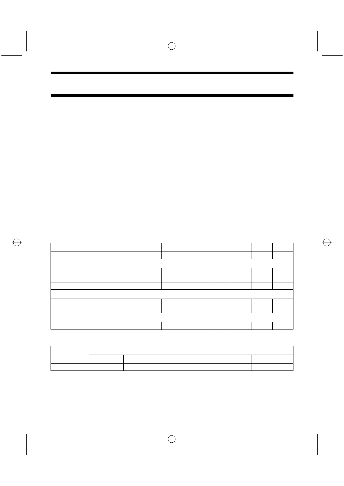
The TDA1302T is a data amplifier and laser supply circuit
for three-beam pick-up detectors applied in a wide range
of mechanisms for Compact Disc and read only optical
systems. The device contains 6 amplifiers which amplify
and filter the focus and radial diode signals and provides
an equalized RF signal suitable for single or double speed
mode; the mode can be switched by means of the speed
control pin. The device can accommodate astigmatic,
single foucault and double foucault detectors and can be
applied to all N-sub laser/monitor diode units even though
the circuit has been optimized for the Philips CDM12
mechanisms and the digital servo controller TDA1301T.
After a single initial adjustment the circuit will maintain
control over the laser diode current thus resulting in a
constant light output power which is independent of
ageing. The IC is mounted in a small-outline package to
enable it to be mounted close to the laser pick-up unit on
the sledge.
TDA1302T
• Low power consumption.
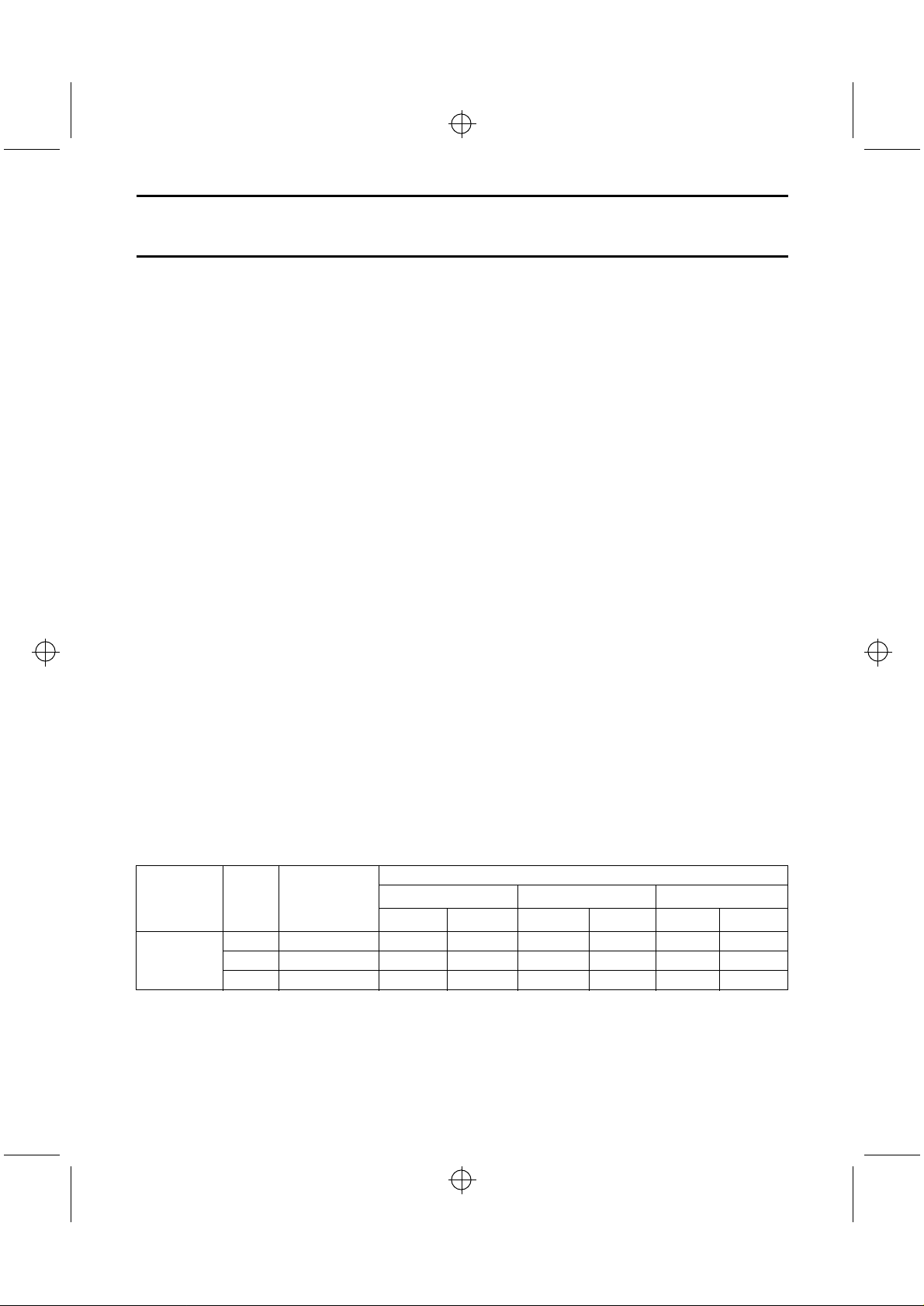
QUICK REFERENCE DATA
SYMBOL PARAMETER CONDITIONS MIN. TYP. MAX. UNIT
V
DD
supply voltage (pin 18) 3.4 − 5.5 V
Diode current amplifiers
G
dn
I
os(d)
B 3 dB bandwidth I
amplification − 1.55 − dB
diode output offset current − − 100 nA
= 1.67 µA 50 − − kHz
i(d)
RFE amplifier (built-in equalizer)
t
d(eq)
t
d(f)
equalization delay fi= 0.3 MHz − 320 − ns
flatness delay double-speed − 5 − ns
Laser supply
I
o(l)
output current V
= 3 V − − −100 mA
DDL
ORDERING INFORMATION
TYPE NUMBER
NAME DESCRIPTION VERSION
PACKAGE
TDA1302T SO24 plastic small outline package; 24 leads; body width 7.5 mm SOT137-1
September 1994 2
Philips Semiconductors Preliminary specification
VV
V
V
V
Fig.1 Schematic diagram for CD player.
Data amplifier and laser supply circuit for
CD player and read only optical systems
SCHEMATIC DIAGRAM
TDA1302T
September 1994 3
TDA1302_1 3 Wed Sep 14 13:30:56 1994
TDA1302_1 4 Wed Sep 14 13:30:56 1994
Fig.2 Block diagram.
Philips Semiconductors Preliminary specification
Data amplifier and laser supply circuit for
CD player and read only optical systems
BLOCK DIAGRAM
TDA1302T
September 1994 4
TDA1302_1 5 Wed Sep 14 13:30:56 1994
Fig.3 Pin configuration.
Philips Semiconductors Preliminary specification
Data amplifier and laser supply circuit for
CD player and read only optical systems
PINNING
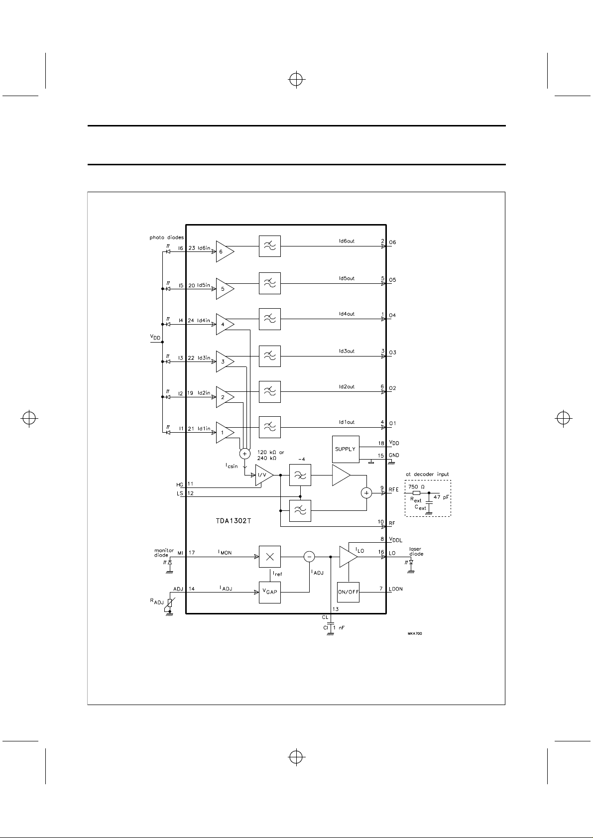
SYMBOL PIN DESCRIPTION
O4 1 output of diode current amplifier 4
O6 2 output of diode current amplifier 6
O3 3 output of diode current amplifier 3
O1 4 output of diode current amplifier 1
O5 5 output of diode current amplifier 5
O2 6 output of diode current amplifier 2
LDON 7 control pin for switching the laser
ON and OFF
V
DDL
RFE 9 equalized output voltage of sum
RF 10 unequalized output
HG 11 control pin for gain switch
LS 12 control pin for speed switch
CL 13 external capacitor
ADJ 14 reference input normally
GND 15 0 V supply; substrate connection
LO 16 current output to the laser diode
MI 17 laser monitor diode input
V
DD
I2 19 photo detector input 2 (central)
I5 20 photo detector input 5 (satellite)
I1 21 photo detector input 1 (central)
I3 22 photo detector input 3 (central)
I6 23 photo detector input 6 (satellite)
I4 24 photo detector input 4 (central)
8 laser supply voltage
signal of amplifiers 1 to 4
connected to ground via a resistor
(ground)
18 amplifier supply voltage
TDA1302T
September 1994 5
TDA1302_1 6 Wed Sep 14 13:30:56 1994
Philips Semiconductors Preliminary specification
Data amplifier and laser supply circuit for
CD player and read only optical systems
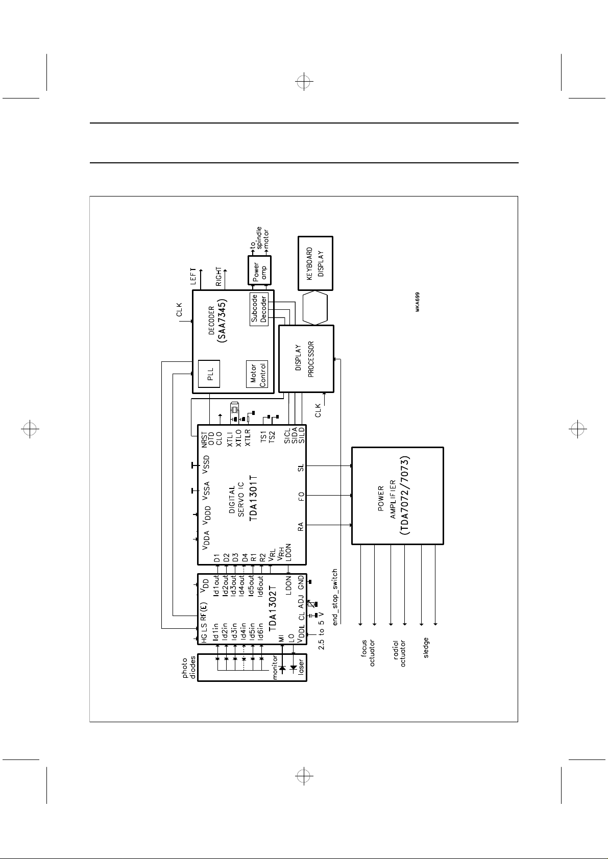
FUNCTIONAL DESCRIPTION
The TDA1302T can be divided into two main sections, the
laser control circuit and the photo diode signal filter and
amplification section.
Laser control circuit
The main function of the laser control circuit is to control
the laser diode current in order to achieve a constant light
output power which is based on the current of the monitor
diode which is continuously monitored. The circuit is built
up into three parts.
The first part is the input stage which compares the
monitor diode current with a current which is 10 times the
value of the adjustable current. The adjustable current is
derived from a bandgap reference source, to be
temperature independent, and can be further adjusted by
the external resistor R
parameters of the laser/monitor diode unit to be used. The
difference is fed to the second part.
The second part is the integrator stage which makes use
of an external capacitor CL. This capacitor has two
different functions.
During switch-on of the laser current, it provides a current
slope of typically: dILO/dt ≅ 10−6/CL (A/s).
After switch-on it ensures that the bandwidth conforms to
the typical formula: fB≅ K × A
where A
represents the AC gain of an extra loop
ext
amplifier, if applied, and K = dI
determined by the laser/monitor unit.
is the average current (pin 17) at typical light
I
MON
emission power of the laser diode.
in order to adapt the circuit to the
ADJ
× 90−9/(CL × I
ext
monitor
/dI
laser
MON
which is
) (Hz).
TDA1302T
The third part is the power output stage, its input being the
integrator output signal. This stage has a separate supply
voltage (V
power consumption by supplying this pin with the minimum
voltage necessary.
It also has a laser diode protection circuit which is enabled
prior to the output drive transistor becoming saturated due
to a large voltage dip on V
lower current from the laser diode, which is normally
followed immediately by an increment of the voltage from
the external capacitor CL, which could cause damage to
the laser diode at the end of the voltage dip. The protection
circuit prevents an increment of the capacitor voltage and
thus offers full protection to the laser diode under these
circumstances.
Photo diode signal filter and amplification section
This section has 6 identical current amplifiers. Amplifiers 1
to 4 are designed to amplify the focus photo diode signals.
Each amplifier has two outputs, an LF output and an
internal RF output. Amplifiers 5 and 6 are used for the
radial photo diode currents and have only an LF output. All
6 output signals are low-pass filtered with a corner
frequency at 65 kHz. The internal RF output signals are
summed together and converted into a voltage by means
of a selectable transresistance of 120 kΩ or 240 kΩ. This
signal is available directly at pin 10, however, there is also
an unfiltered signal available at pin 9. The equalization
filter used has 2 different filter curves, one for single-speed
mode and one for double-speed mode.
) thereby offering the possibility of reduced
DDL
. Saturation will result in a
DDL
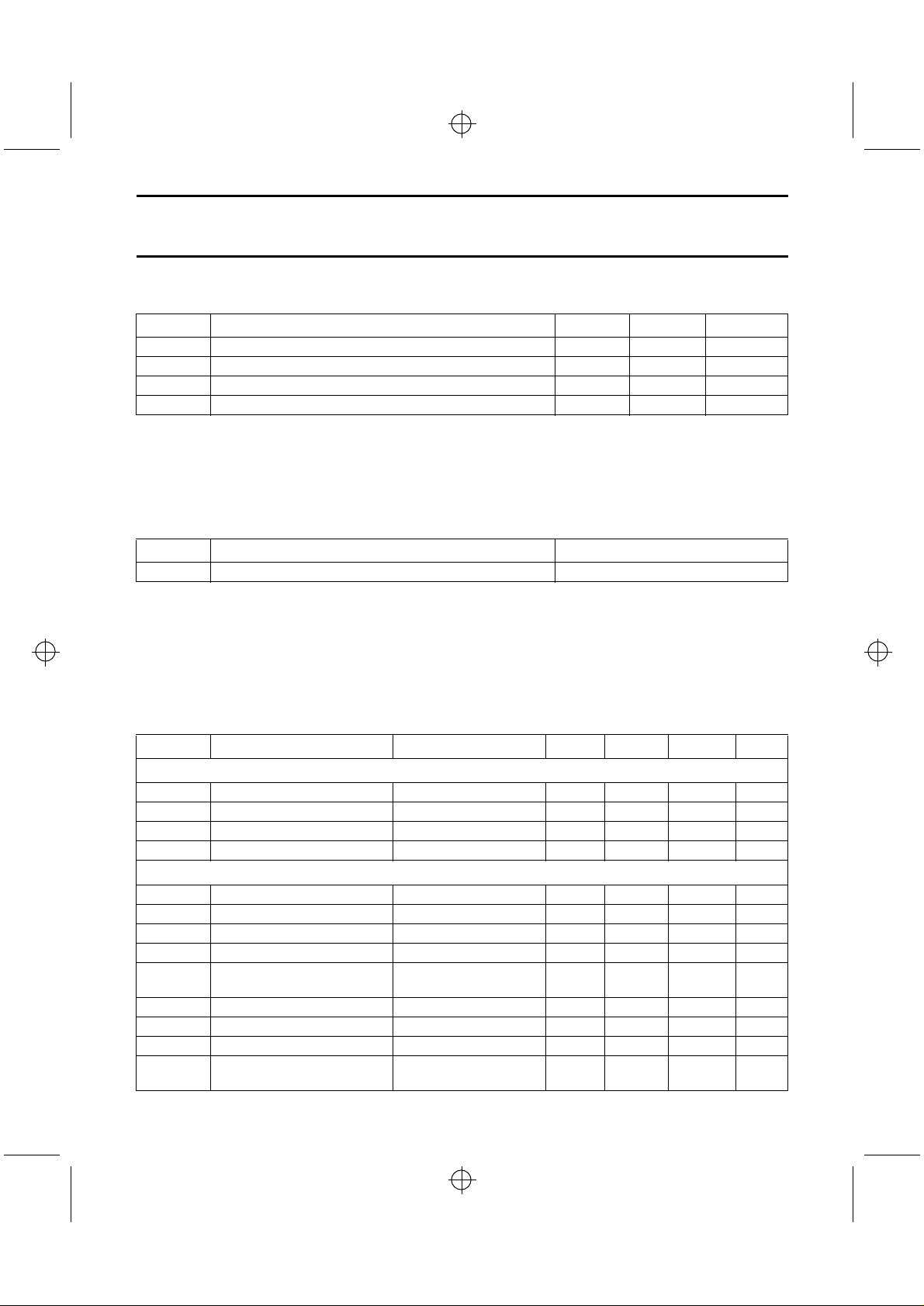
Table 1 Operational modes.
IF NOT
SWITCH PIN
CONNECTED
DEFAULT
GAIN SPEED LASER
HIGH LOW SINGLE DOUBLE ON OFF
HG 1 1 0 X X X X
Control pin
LS 1 X X 1 0 X X
LDON 1 X X X X 1 0
Note
1. Where X = don’t care.
September 1994 6
MODE
(1)
TDA1302_1 7 Wed Sep 14 13:30:56 1994
Philips Semiconductors Preliminary specification
Data amplifier and laser supply circuit for
CD player and read only optical systems
TDA1302T
LIMITING VALUES
In accordance with the Absolute Maximum Rating System (IEC 134).
SYMBOL PARAMETER MIN. MAX. UNIT
V
DD
P
tot
T
stg
T
amb
supply voltage − 8.0 V
total power dissipation − 300 mW
storage temperature −65 +150 °C
operating ambient temperature −40 +85 °C
HANDLING
Classification A: human body model; C = 100 pF; R = 1500 Ω; V = ± 2000 V.
Charge device model: C = 200 pF; L = 2.5 µH; R = 0 Ω; V = 250 V.
THERMAL RESISTANCE
SYMBOL PARAMETER THERMAL RESISTANCE
R
th j-a
from junction to ambient in free air 60 K/W
QUALITY SPECIFICATION
In accordance with
“SNW-FQ-611 part E”
Reference Handbook”
. The handbook can be ordered using the code 9398 510 63011.
. The numbers of the quality specification can be found in the
“Quality
CHARACTERISTICS
VDD= 3.4 V; V
(R
= 750 Ω, C
ext
= 2.5 V; T
DDL
= 47 pF) at pin 9; unless otherwise specified.
ext
= 25 °C; R
amb
= 48 kΩ; HG = logic 1; LS = logic 1; with an external LP filter
ADJ
SYMBOL PARAMETER CONDITIONS MIN. TYP. MAX. UNIT
Supply
I
DD
V
DD
V
DDL
P
diss
amplifier supply current laser OFF − 8 − mA
amplifier supply voltage 3.4 − 5.5 V
laser control supply voltage 2.5 − 5.5 V
power dissipation laser OFF; VDD= 3.4 V − 27 − mW
Diode current amplifiers (1 to 6)
I
i(d)
N
eq
V
i(d)
V
o(d)
G
dn
I
os(d)
Z
o(d)
B 3 dB bandwidth I
G
mm
diode input current note 1 − − 10 µA
equivalent noise input − 1 − pA/√Hz
diode input voltage I
= 1.67 µA − 0.9 − V
i(d)
diode output voltage −0.2 − VDD− 1 V
amplification I
diode output offset current I
output impedance Idi= 1.67 µA; V
mismatch in amplification Idi= 1.67 µA;
= 1.67 µA;
i(d)
V
= 0 V; note 2
o(dn)
= I
csin
i(d)
= 0; note 3 − − 100 nA
tsin
o(dn)
= 1.67 µA 50 68 − kHz
1.43 1.55 1.67 dB
= 0 V 500 − − kΩ
− − 3 %
V
= V
o(dn)
o(dm)
September 1994 7
 Loading...