

Philips tda1301 DATASHEETS

INTEGRATED CIRCUITS
DATA SH EET
TDA1301T
Digital servo processor (DSIC2)
Product specification
File under Integrated Circuits, IC01
Philips Semiconductors
January 1996

Philips Semiconductors Product specification
Digital servo processor (DSIC2) TDA1301T
FEATURES
The DSIC2 realizes the following servo functions:
• Diode signal preprocessing
• Focus servo loop
• Radial servo loop
• Sledge motor servo loop
• Three-line serial interface via the microcontroller
The other features include:
• Full digital signal processing
• Low power consumption, down to 30 mW
• Low voltage supply 3 to 5.5 V
• Integrated analog-to-digital converters and digital servo
loop filters
• Double speed possible
• Easy application
– Single supply voltage
– Small number of external components; only
6 decoupling capacitors
– Flexible system oscillator circuitry
– Usable for single/double Foucault and astigmatic
focus
– Full automatic radial error signal initialization offset
control and level initialization for track position
indicator
– No external adjustments required; no component
ageing
– Wide range of adjustable servo characteristics
– Simple 3-line serial command interface
– 28-pin SO package
– Great flexibility towards different CD mechanisms
– Full and transparent application information
• High robustness/shock insensitivity
– Sophisticated track-loss (TL) detection mechanism
– Fast focus restart procedure
– Extended radial error signal
– Adjustable radial shock detector
– Defect drop-out detector
• Fully automatic jump procedure for radial servo
• Automatic focus start-up procedure and built-in FOK
(Focus OK)
• Fast radial jump or access procedure
• Self-operational servo-control without continuous
communication via the microcontroller
• Direct communication to photodiode optics; no external
preprocessing.
GENERAL DESCRIPTION
The TDA1301T is a fully digital servo processor which has
been designed to provide all servo functions, except the
spindle motor control, in two-stage three-spot compact
disc systems. The device offers a high degree of
integration, combined with the low additional cost of
external components. The servo characteristics have a
wide range of adjustment via a three-line serial interface.
This offers an enormous flexibility with respect to
applications for different CD mechanisms. The circuit is
optimized for low-power low-voltage applications.
QUICK REFERENCE DATA
SYMBOL PARAMETER CONDITIONS MIN. TYP. MAX. UNIT
V
DDD
V
DDA
I
DDD
I
DDA
I
DDD(q)
I
i(cd)
I
i(sd)
P
tot
T
amb
digital supply voltage 3.0 − 5.5 V
analog supply voltage 3.0 − 5.5 V
digital supply current − 5 − mA
analog supply current − 5 − mA
digital quiescent supply current −−10 µA
central diode input currents (D1 to D4) note 1 −−15.8 µA
satellite diode input currents (R1 and R2) note 1 −−7.9 µA
total power dissipation − 50 − mW
operating ambient temperature −40 − +85 °C
Note
= 4.2336 MHz; VRL = 0 V; VRH = 2.5 V (externally applied).
1. f
sys
January 1996 2
Philips Semiconductors Product specification
Digital servo processor (DSIC2) TDA1301T
ORDERING INFORMATION
EXTENDED TYPE
NUMBER
TDA1301T 28 SO28L plastic SOT136A
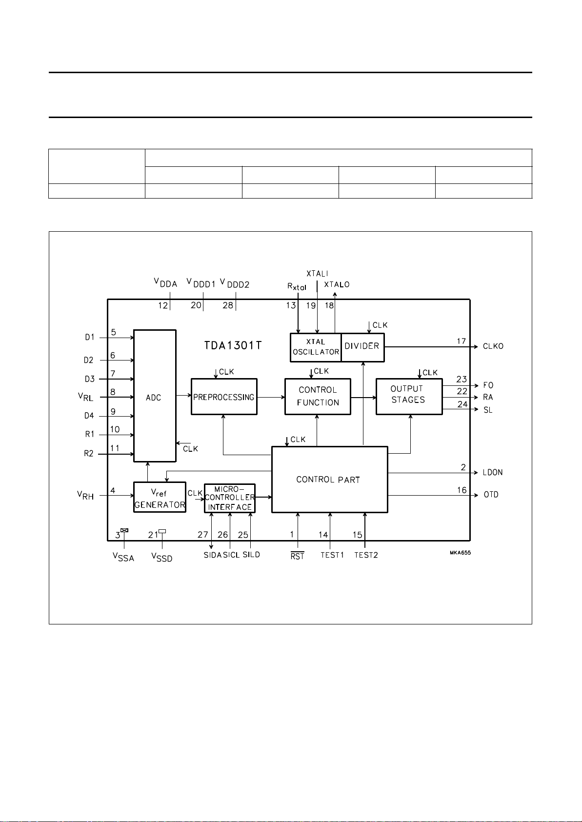
BLOCK DIAGRAM
PINS PIN POSITION MATERIAL CODE
PACKAGE
January 1996 3
Fig.1 Block diagram.
Philips Semiconductors Product specification
Digital servo processor (DSIC2) TDA1301T
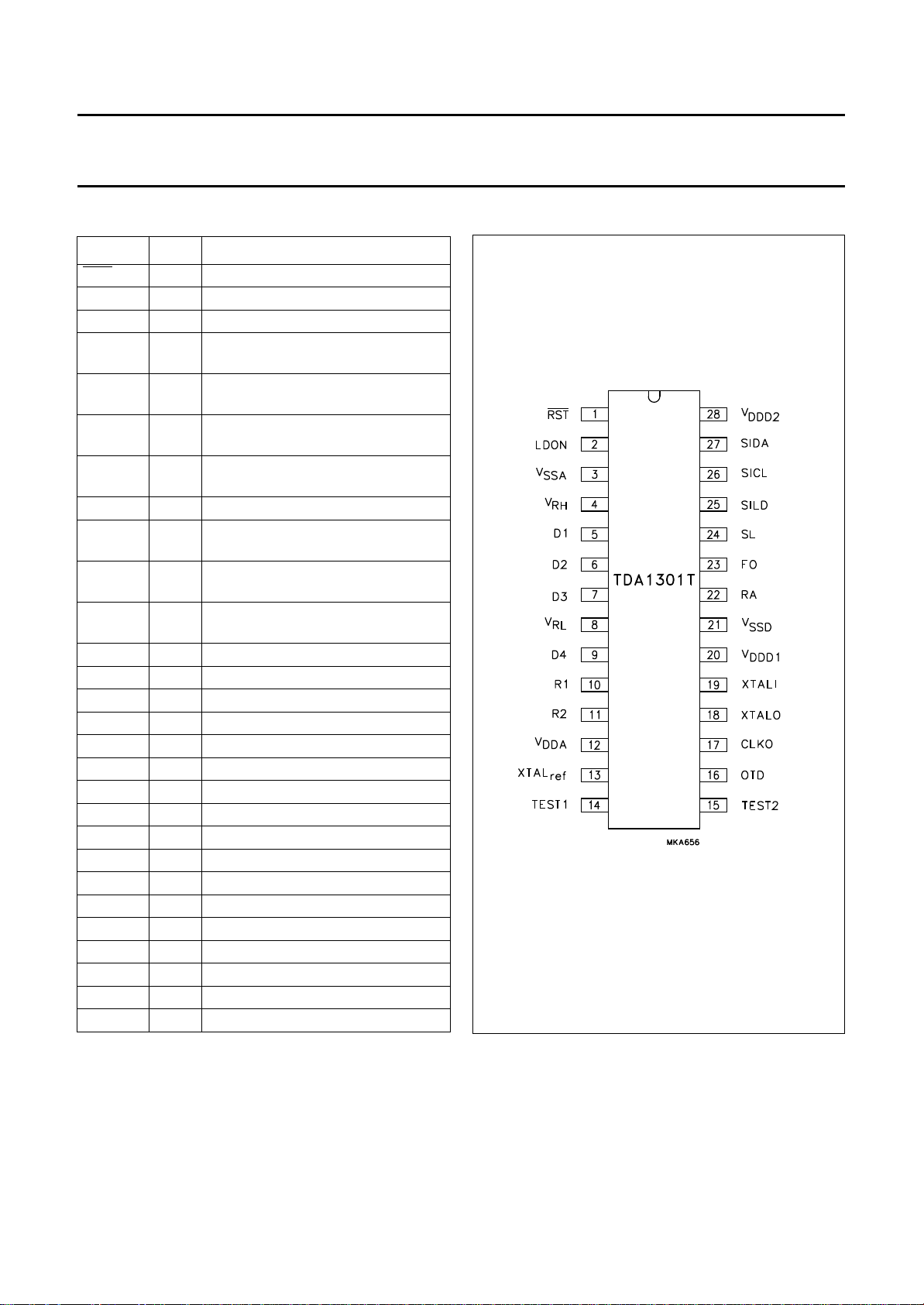
PINNING
SYMBOL PIN DESCRIPTION
RST 1 reset input (active LOW)
LDON 2 laser drive on output
V
SSA
V
RH
D1 5 unipolar current input
D2 6 unipolar current input
D3 7 unipolar current input
V
RL
D4 9 unipolar current input
R1 10 unipolar current input
R2 11 unipolar current input
V
DDA
XTAL
ref
TEST1 14 test input 1
TEST2 15 test input 2
OTD 16 off-track detector output
CLKO 17 clock output
XTALO 18 oscillator output
XTALI 19 oscillator input
V
DDD1
V
SSD
RA 22 radial actuator output
FO 23 focus actuator output
SL 24 sledge output
SILD 25 serial interface load input
SICL 26 serial interface clock input
SIDA 27 serial interface data input/output
V
DDD2
3 analog ground
4 reference input for reference voltage
generator
(central diode signal input)
(central diode signal input)
(central diode signal input)
8 reference input for ADC
(central diode signal input)
(satellite diode signal input)
(satellite diode signal input)
12 analog supply voltage
13 oscillator reference input
20 digital power supply 1
21 digital ground
28 digital power supply 2
Fig.2 Pin configuration.
January 1996 4
Philips Semiconductors Product specification
Digital servo processor (DSIC2) TDA1301T
FUNCTIONAL DESCRIPTION
Three spots front-end
The photo detector in a two-stage three-spots compact
disc system normally contains six discrete elements. Four
of these elements (in the event of single Foucault: three
elements) carry the central aperture (CA) signal while the
other two elements (satellite signals) carry the radial
tracking information. Besides the HF signal, which is finally
applied to both of the audio channels, the central aperture
also contains information for the focus servo loop. To
enable the HF signal to be processed, the frequency
contents of the central aperture signal must be divided into
an HF data part and an LF servo part. The HF signal is
processed outside the DSIC2 by the TDA1302 or a
discrete amplifier-equalizer. The necessary crossover
point, to extract the LF servo part, is compensated for in
the amplifier.
Diode signal processing
The analog signals from the photo detectors are converted
into a digital representation using analog-to-digital
converters. The ADCs are designed to convert unipolar
currents into a digital code. The dynamic range of the input
currents is adjustable within a given range and is
dependent on the ADC input reference voltages V
RL
and
VRH. The maximum current for the central diodes signals
is given in equation (1).
I
i max()
f
VRHVRL–()1.5 106–×××= µA[]
sys
(1)
The maximum current for the satellite signals is given in
equation (2).
I
i max()
V
RH
f
VRHVRL–()0.75 106–×××= µA[]
sys
(2)
is generated internally. There are four different levels
(1.0, 1.5, 2.0 and 2.5 V) which can be selected under
software control. In the application VRL is connected to
V
. It is also possible to drive VRH with an external
SSA
voltage source but in this situation the internal voltage
source has to be switched off (software controlled).
Signal conditioning
The digital codes retrieved from the ADCs are applied to
logic circuitry to obtain the various control signals. The
signals from the central aperture detectors are processed
so that the normalized focus error signal (FE) given in
equation (3) is realized:
FE
n
D1 D2–
---------------------D1 D2+
D3 D4–
–=
---------------------D3 D4+
(3)
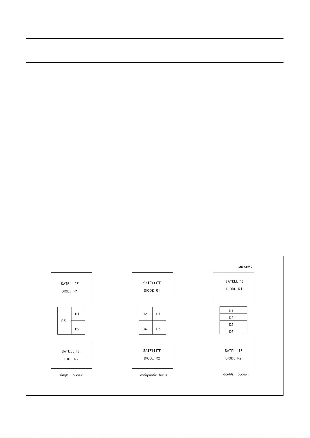
Where the detector set-up is assumed to be as illustrated
in Fig.3.
January 1996 5
Fig.3 Diode configuration.
 Loading...