

Philips TDA1170N Service Manual

TECHNICAL NOTE
VERTICALDEFLECTION CIRCUITS FOR TV & MONITOR
By Alessandro MESSI
SUMMARY Page
1 INTRODUCTION. . . . . . . . . . . . . . . . . . . . . . . . . . ............................. 2
2 OSCILLATOR. . . ...................................................... 3
3 RAMP GENERATOR . . . . . . . . . . . . ....................................... 4
4 BLANKINGGENERATOR AND CRT PROTECTION. .......................... 4
5 POWERAMPLIFIERSTAGE . . . . . . . . . . . . . . . . . . . . . . . . . . ................... 4
6 THERMAL PROTECTION . . . . . . . . . . . . . . . . . . . . . .. . . . . . ................... 6
7 FLYBACKBEHAVIOUR . ................................................ 6
8 CURRENT- VOLTAGECHARACTERISTICSOF THE RECIRCULATING DIODES . . 11
9 CALCULATIONPROCEDURE OF THE FLYBACKDURATION . . . . . . . . . . . ....... 12
10 APPLICATIONINFORMATION . . ......................................... 12
11 SUPPLY VOLTAGECALCULATION . . . . . . . . . . . . . . . . .. . .. .. . . .. . . . . . . . . . . . . 14
12 CALCULATIONOF MIDPOINTAND GAIN . . . . .. . . . . . . . . . ................... 17
13 MONITOR APPLICATIONS . . . . . ......................................... 20
14 POWER DISSIPATION. . . . . . . . . .. . . . . . . . . . . ............................. 20
15 BLANKING PULSE DURATION ADJUSTMENT . . . . .. . ....................... 21
16 LINEARITY ADJUSTMENT. . ............................................. 21
17 FACILITIES AND IMPROVEMENTS . . . . . . . . . . . . . . . . . . . . ................... 22
18 GENERAL APPLICATION AND LAYOUT HINTS. ............................. 23
19 REFERENCES. . . . . ................................................... 23
AN373/0694
1/23
VERTICALDEFLECTION CIRCUITS FOR TV & MONITOR
1 - INTRODUCTION
In a general way we can define vertical stages
circuits able to deliver a current ramp suitable to
drive the verticaldeflection yoke.
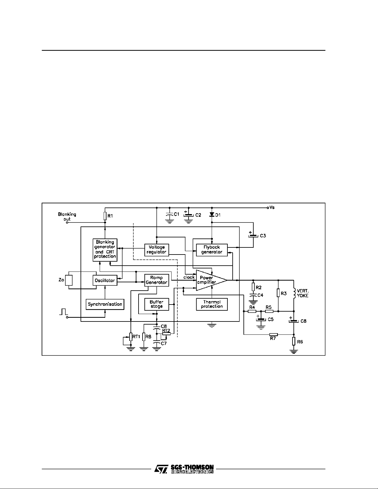
In Figure1 is representedthemore generalpossible blockdiagram of a deviceperformingthe vertical deflection.
Such a device will be called ”complete vertical
stage” because it can be simply driven by a synchronizationpulseand it comprises allthe circuitry
necessaryto performtheverticaldeflectionthatis:
oscillator, voltageramp generator,blanking gene-
tor, outputpower and flybackgenerator.
At the right side of the dotted line in Figure 1 is
represented the circuitry characterizing a ”vertical
output stage”. This kind of device comprises only
Figure 1 : BlockDiagram of a General Deflection Stage
the power stages and it has to be driven by a
voltage sawtooth generated by a previous circuit
(for examplea horizontaland verticalsynchronization stage.
In the first class there are the following devices :
TDA1170D, TDA1170N, TDA1170S, TDA1175,
TDA1670A, TDA1675, TDA1770A, TDA1872A,
TDA8176.
In thesecondclassthereare:TDA2170,TDA2270,
TDA8170, TDA8172, TDA8173, TDA8175,
TDA8178,TDA8179.
There is also a thrid class of vertical stages compraisingthevoltagerampgeneratorbutwithoutthe
oscillator; these circuits must be driven by an already synchronizedpulse. In this third class there
are : TDA1771and TDA8174.
2/23
AN373-01.EPS
VERTICALDEFLECTION CIRCUITS FOR TV & MONITOR
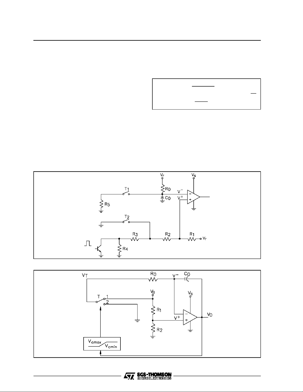
2 - OSCILLATOR
There are two different kinds of oscillator stages
used in SGS-THOMSONcomplete verticaldeflections, one is used in TDA1170D, TDA1170N,
TDA1170S, TDA1175 and TDA8176, the other in
TDA1670A,TDA1675,TDA1170AandTDA1872A.
The principle of thefirst kind ofoscillator is represented in Figure2.
The followingexplanationswillbethemoregeneral
possible;we shall informthe readerwhenwe refer
to a particulardevice.
When the switchesT
capacitor charges exponentiallythrough ROto the
value V
tors R
+
(MAX)
1,R2,R3
determined by the integratedresis-
and R4. At this point the switches
are closed, short-circuitingR
age atthenon-invertinginputbecomesV
capacitor C
dischargesto this value through the
O
Figure 2 : First Kind of Oscillator Stage
and T2are opened the C
1
andR4, so the volt-
3
+
(MIN)
.The
integrated resistor R
.
5
The free running frequency can be easily calculated resultingin :
+
V
−V
R
TO= RO⋅ CO⋅ log
+ R5⋅ C
O
⋅log
VR− V
+
V
(MAX)
+
V
(MIN)
(MIN)
+
(MAX)
(1)
with RO= 360 kΩ and CO= 100 nF, it results in
43.7Hz.
O
Theoscillatorsynchronizationis obtainedreducing
the superior threshold V
resistor when a vertical synchronizationpulse
R
4
+
short-circuiting the
(MAX)
occurs.
The second kind of oscillator is represented in
Figure3.
1
f
=
O
T
O
Figure3 : Second Kind of OscillatorStage
AN373-02.EPS
AN373-03.EPS
3/23

VERTICALDEFLECTION CIRCUITS FOR TV & MONITOR
When the switch T is in position 2, a constant
current I
with avoltageramp. When thevoltage V
V
O(MAX)
currentI
=V-/ROflows through COchargingit
CO
reaches
O
, T passes in position 1, so a constant
=(VB-V-)/ROdischargesthe capaci-
CO
tor causingthe inversionof the voltagerampslope
at the output V
reaches the value V
V
O
( t ). The dischargesstops when
O
and the cycle takes
O(MIN)
place again.
It ispossibletocalculatethe freerunningfrequency
withthe following formula :
f
O
TO=
with V
(V
+
O(MAX)
O(MAX)
( V
O(MAX)
− V
− V
-V
) ⋅ R
O(MIN)
−
V
O(MIN)
VB− V
O(MIN)
O⋅CO
) ⋅ R
⋅ C
O
−
O
= 3.9V, VB= 6.5V, V
(2)
= 0.445V,RO= 7.5kΩ and CO= 330nF it results
= 43.8Hz.
in : f
O
Theoscillatorsynchronizationisstill obtainedinthe
above mentioned way.
In order to guarantee a minimum pull-in range of
14Hz the threshold value has been chosen in
= 4.3V.
V
P
The spread of the free running frequency in this
kind of oscillator is very low because it mainly
dependsfromthethresholdvaluesV
O(MAX),VO(MIN)
and V-that are determinedby resistor rates that
can be done very precise.
3 - RAMP GENERATOR
The rampgeneratoris conceptuallyrepresentedin
Figure 4.
The Voltage ramp is obtained charging the group
R
Itiseasy tocalculatethevoltageV
and C2with a constant current IX.
1,C1
RAMP
Thatresults
in :
1
V
RAMP
where V
(t)=(V
(MIN)
− R1⋅ IX) e
(MIN)
is the voltage in A when the charge
−
starts and Cis the seriesof C
TheresistorR
isnecessarytogivea ”C correction”
1
⋅ C
R
1
and C2.
1
+ R1⋅ I
(3)
X
to the voltage ramp. Theramp amplitude is determined by I
X=VREG/P1
,sothe potentiometerP1is
necessaryto perform the height control.
The voltage ramp is then transferred on a low
impedencein B througha bufferstage.
TheP2 potentiometerconnectedbetweenD andB
performstheramplinearitycontrolor”Scorrection”
that is necessaryto havea correct reproductionof
the imageson the TV set.
The voltage ramp in B grows upuntil the switch T
is closedby a clockpulse coming from the oscillator; in this way the capacitors discharge fastly to
that is dependent upon the saturation volt-
V
(MIN)
age of the transistor thatrealizes the switch.
At this point the exponential charge takes place
again.
4 - BLANKING GENERATOR AND CRT PROTECTION
-
This circuit senses the presenceof theclockpulse
coming from the oscillator stage and the flyback
pulse on the yoke. If both of them are present a
blankingpulse is generatedable to blank the CRT
duringthe retraceperiod.Thedurationof thispulse
is the same of the one coming from the oscillator.
If for any reason the verticaldeflection would fail,
for instance for a short circuit or an open circuitof
the yoke,theabsenceof theflybackpulse puts the
circuitinsuch a condition thata continuousvertical
blanking is generated in order to protect the CRT
againsteventual damages.
This circuit is available only in the following devices :TDA1670A, TDA1675, TDA1770A and
TDA1872A.
The stages we will consider startingfrom this point
are common both to complete vertical stages and
verticaloutput stages.
5 - POWERAMPLIFIER STAGE
This stage can be divided into two distinct parts :
the amplifiercircuitand the output power.
The amplifieris realizedwith a differentialcircuit; a
schematicdiagram is representedin Figure 5.
The open-loop gain of the circuit is variable from
60dB to 90dBfor the different integratedcircuits.
The compensation capacitor C determines the
dominantpole ofthe amplifier. In orderto obtain a
dominantpolein the rangeof 400Hz,thecapacitor
must be of about 10pF.
1
4/23
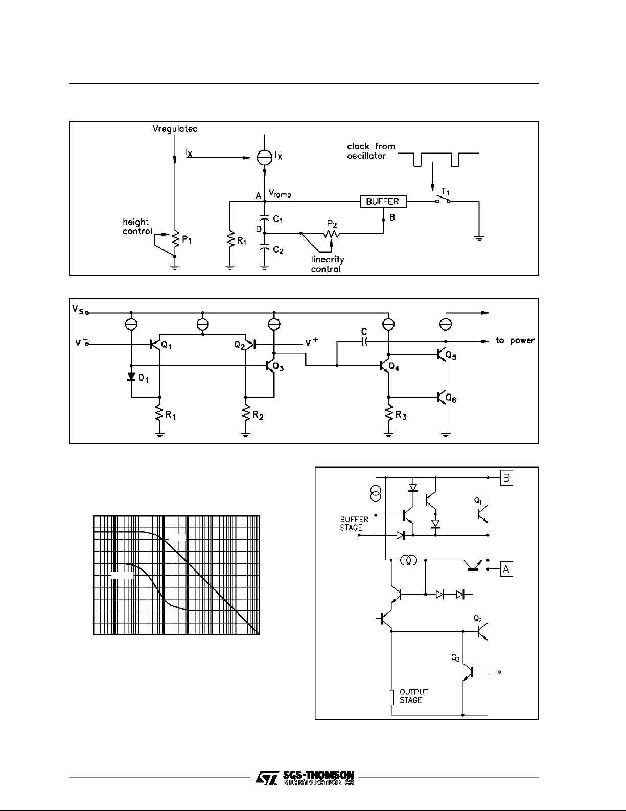
Figure4 : Ramp Generator
Figure5 : AmplifierStage
VERTICALDEFLECTION CIRCUITS FOR TV & MONITOR
AN373-04.EPS
As an examplein Figure 6 is representedtheboole
diagram of the amplifier open loop gain for
TDA8172.
Figure 6 : AmplifierOpen Loop Gainand Phase
6
90
45
0
-45
-90
- 135
7
100
80
60
PHASE
GAIN(dB)
40
20
0
1 1010101010 1010
GAIN
23
FREQUENCY, f (Hz)
4
5
The output power stage is designed in order to
delivertotheyokeaverticaldeflectioncurrentfrom
1 to2Apeak,dependinguponthedifferentdevices,
and able to support flyback voltages up to 60V. A
typical output stage is depictedin Figure 7.
AN373-05.EPS
Figure7 : Power Stage
PHASE (Degrees)
AN373-06.EPS
AN373-07.EPS
5/23
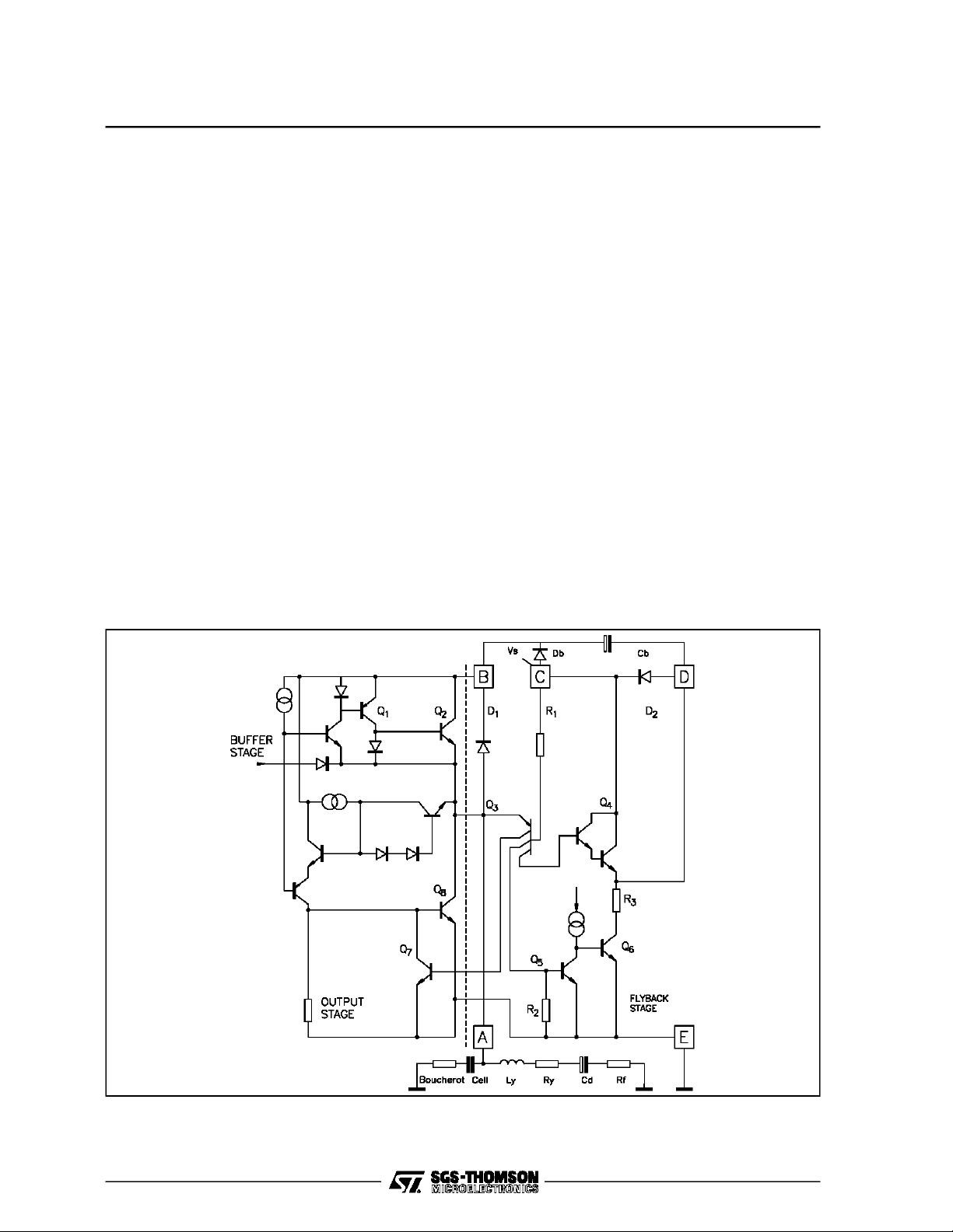
VERTICALDEFLECTION CIRCUITS FOR TV & MONITOR
The upperpowertransistorQ
conductsduringthe
1
first part of the scanning period when the vertical
deflectioncurrentisflowingfromthesupplyvoltage
into theyoke;whenthecurrent becomesnegative,
that isit comesout of the yoke,it flows throughthe
lower power transistor Q
.The circuit connected
2
between the two output transistorsis necessaryto
avoid distortion of the current at the crossing of
zero, when Q
When the flybackbegins, Q
is turned off and Q2isturned on.
1
isswitched-offby Q
2
in order to makeit ableto support the highvoltage
of the flyback pulse.
The circuitbehaviourduring flybackis explainedin
chapter 7.
6 - THERMALPROTECTION
Thethermalprotectionisavailableinallthe devices
except theTDA1170 family andthe TDA8176.
This circuit is usefull to avoid damages at the
integrated circuit due to a too high junction temperaturecausedby an incorrectworkingcondition.
It is possible to sense the silicon temperature because the transistorV
varies of - 2 mV/oC, so a
BE
Figure8 : Output Power and FlybackStages
temperature variation can be reconducted to a
voltagevariation.
If the temperature increases and it is reaching
o
C, theintegratedcircuit output isshut downby
150
puttingoff the current sources of the power stage.
7 - FLYBACK BEHAVIOUR
In orderto obtain sufficiently short flyback times,a
3
voltage greather than the scanning voltage must
be appliedto the deflection yoke.
By using a flyback generator, the yoke is only
supplied with a voltage close to double the supply
during flyback.
Thus, the power dissipated is reduced to approximately one thirdand the flyback time is halfed.
The flyback circuit is shown in Figure 8 together
with the powerstage.
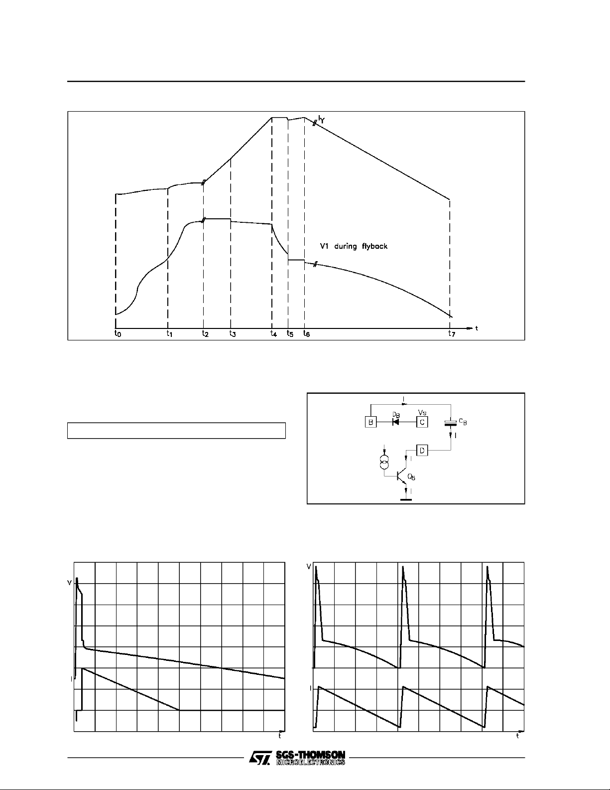
Figure 9 showsthe circuit behaviuor, to show operation clearly. Thegraphsare not drawnto scale.
Certainapproximationsare made in the analysisin
order to eliminate electrical parametersthatdo not
significantlyinfluence circuit operations.
6/23
AN373-08.EPS
VERTICALDEFLECTION CIRCUITS FOR TV & MONITOR
Figure9 : Current in theYokeand VoltageDrop on The Yoke during VerticalDeflection
AN373-09.EPS
a) Scan period (t
During scanning Q
causes Q
to saturate.
6
):Figure10
6-t7
3,Q4
and Q5are off and this
A current from the voltage supply to ground flows
through D
and Q6charging the CBcapacitor
B,CB
up to :
VCB=VS-VDB-VQ
6SAT
(4)
At the end of this period the scan current has
reacheditspeakvalue (I
yoke to the device. At the same time V
) andit is flowingfromthe
P
A
has
reached its minimum value.
In Figures11 and 12are depictedthe voltagedrop
Figure 11 : Voltage Drop on the Yoke and Cur-
rent Flowingthrough D
B
V = 10V/div. - I = 0.5A/div.
t = 2ms/div.
on the yoke and the currents flowing through D
and the yoke.
Figure10 : Circuit involvedduring Scan Period
Figure12 : Voltage Drop on the Yoke and Cur-
rent Flowingthroughthe Yoke
V = 10V/div. - I = 1A/div.
t = 5ms/div.
B
AN373-10.EPS
AN373-11.EPS
AN373-12.EPS
7/23
VERTICALDEFLECTION CIRCUITS FOR TV & MONITOR
b) Flyback starting (t
Q
, that was conductingthe - IPcurrent, is turned
8
):Figure13
0-t1
off by the bufferstage.
The yoke, charged to I
flow partially through the Boucherot cell (I
partially through D
, now forcesthis current to
P
and Q6(I2).
1,CB
) and
1
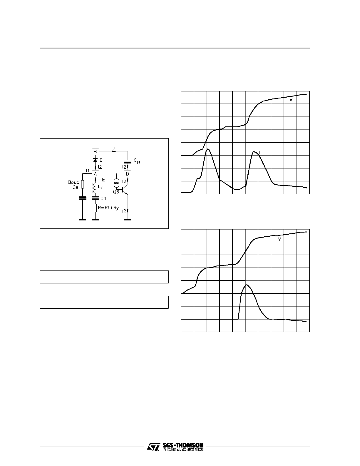
In Figures 14, 15 and 16 are represented the
currents flowing through the yoke, the Boucherot
cell and D1.
Figure13:CircuitinvolvedduringFlybackStarting
c) Flyback starting (t
When the voltage drop at pin A rises over V
1-t2
)
S,Q3
turns on and this causes Q4and Q5to saturate.
ConsequentlyQ
turnsoff.
6
During this period the voltageat pinD is forcedto :
Figure14 : Voltage Drop on the Yoke and Cur-
rent Flowingthroughthe Boucherot
Cell- V = 10V/div.
I = 1A/div. - t = 1µs/div.
Figure15 : Voltage Drop on the Yoke and Cur-
rent FlowingthroughD
1
V = 10V/div. - I = 1A/div.
AN373-13.EPS
t=1µs/div.
AN373-14.EPS
VD=VS-VQ
4SAT
(5)
Therefore the voltage at pinB becomes :
VB=VCB+V
D
(6)
The yokecurrent flowsintheBoucherotcelladded
to anothercurrentpeakflowingfrom V
(Figures14 and 15).
C
B
8/23
viaQ4and
S
AN373-15.EPS
 Loading...