

Philips TDA1170 Service Manual

LOW-NOISE TV VERTICALDEFLECTIONSYSTEM
.
COMPLETE VERTICAL DEFLECTION SYSTEM
.
LOW NOISE
.
SUITABLE FOR HIGH DEFINITION MONITORS
DESCRIPTION
The TDA1170Dis a monolithicintegratedcircuitin
a 16-leaddualin-line plasticpackage.Itis intended
for use in black and whiteandcolourTV receivers.
Low-noise makes this deviceparticularly suitable for use in monitors. The functions incorpo-
rated are : synchronization circuit, oscillator and
ramp generator,highpower gain amplifier,flyback
generator,voltageregulator.
TDA1170D
DIP16
(Plastic Package)
ORDER CODE : TDA1170D
PIN CONNECTIONS
POWER AMPLIFIER OUTPUT
REGULATED VOLTAGE
December 1992
RAMP OUTPUT
SUPPLY VOLTAGE
FLYBACK
GROUND
GROUND
POWER AMPLIFIER
SUPPLY VOLTAGE
1
2
3
4
5
6
7
8
16
15
14
13
12
11
10
RAMP GENERATOR
COMPENSATION
AMPLIFIER INPUT
GROUND
GROUND
OSCILLATOR
SYNC. INPUT
HEIGHT ADJUST
9
1170D-01.EPS
1/8
TDA1170D
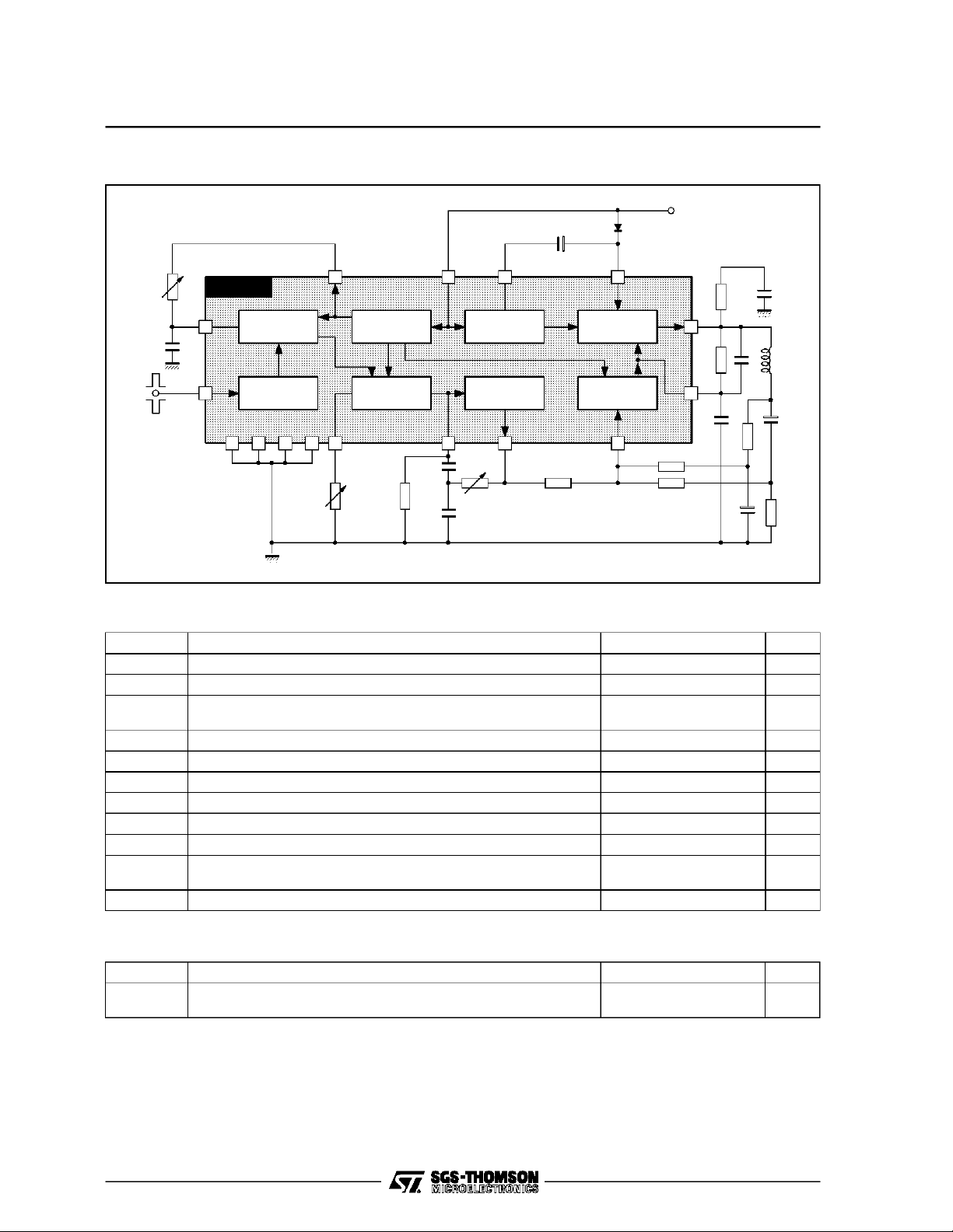
BLOCK DIAGRAM
+V
S
FREQ
SYNC
TDA1170D
OSCILLATOR
11
10
4 5 12 13
SYNC
CIRCUIT
87
VOLTAGE
REGULATOR
RAMP
GENERATOR
916 14
HEIGHT
2
LINEARITY
3
FLYBACK
GENERATOR
BUFFER
STAGE
1
POWER
AMPLIFLIER
PREAMPLIFLIER
6
15
ABSOLUTEMAXIMUM RATINGS
Symbol Parameter Value Unit
V
V
6,V7
V
I
I
I
I
I
I
10
P
T
stg,Tj
S
14
o
o
o
3
3
tot
Supply Voltage at Pin 2 35 V
Flyback Peak Voltage 60 V
Power Amplifier Input Voltage + 10
– 0.5
Output Peak Current (non repetitive) at t = 2msec 2 A
Output Peak Current at f = 50Hz t ≤ 10µsec 2.5 A
Output Prak Current at f = 50Hz t > 10µsec 1.5 A
Pin 3 DC Current at V6<V
2
Pin 3 Peak to Peak Flyback Current for f = 50Hz, t
≤ 1.5msec 1.8 A
fly
100 mA
Pin 10 Current ± 20 mA
Power Dissipation : at T
at T
=90°C
tab
=70°C (free air)
amb
4.3
1
Storage and JunctionTemperature – 40 to 150 °C
YOKE
1170D-02.EPS
V
V
W
W
1170D-01.TBL
THERMALDATA
Symbol Parameter Value Unit
R
th j–case
R
th j–amb
* Obtained with pins 4, 5,12, 13 soldered to printed circuit with minimized copper area.
Thermal Resistance Junction–pins
Thermal Resistance Junction-ambient
2/8
Max
Max
14
80
°C/W
°C/W*
1170D-02.TBL
TDA1170D
ELECTRICAL CHARACTERISTICS
(refer to the testcircuits, V
=35V, T
S
DC CHARACTERISTICS
Symbol Parameter Test Conditions Min. Typ. Max. Unit Fig.
I
2
I
7
–I
11
–I
14
–I
16
–I
16
∆I
16
I
16
V
S
V
1
V
3
V
6
V
6L
V
6H
V
8
V
9
∆V
8
,
∆V
S
V
14
R10 Pin 10 Input Resistance V
Pin 2 Quiescent Current I3=0 7 14 mA 1b
Pin 7 Quiescent Current I6=0 8 17 mA 1b
Oscillator Bias Current V11= 1V 0.1 1 µA1a
Amplifier Input Bias Current V14=1V 1 10 µA1b
Ramp GeneratorBias Current V16= 0 0.02 0.3 µA1a
Ramp GeneratorCurrent I9=20µA, V16= 0 18.5 20 21.5 µA1b
Ramp GeneratorNon-linearity ∆V16= 0to 12V, I9=20µA 0.2 1 % 1b
Supply Voltage Range 10 35 V –
Pin 1 Saturation Voltage to Ground I1= 1mA 1 1.4 V –
Pin 3 Saturation Voltage to Ground I3= 10mA 300 450 mV 1a
Quiescent Output Voltage Vs= 10V
Output Saturation Voltage to Ground – I6= 0.1A
Output Saturation Voltage to Supply I6= 0.1A
Regulated Voltage at Pin 8 6.1 6.5 6.9 V 1b
Regulated Voltage at Pin 9 I9=20µA 6.2 6.6 7 V 1b
∆V
9
Regulated Voltage Drift with Supply
Voltage
∆V
S
Amplifier Input Reference Voltage 2.07 2.2 2.3 V –
=25oC, unless otherwisespecified)
amb
R1 = 1kΩ,R2=1kΩ
V
= 35V
s
R1 = 3kΩ,R2=1kΩ
= 0.8A
–I
6
= 0.8A
I
6
= 10 to 35V 1 mV/V 1b
∆V
S
≤ 0.4V 1 MΩ 1a
10
4.1 4.4 4.75 V 1a
8.3 8.8 9.45 V 1a
0.9
1.2
1.9
2.3VV
1.4
2.1
2.8
3.2VV
1c
1c
1d
1d
1170D-03.TBL
3/8
 Loading...