

Philips TDA1074A Datasheet

INTEGRATED CIRCUITS
DATA SH EET
TDA1074A
Dual tandem electronic
potentiometer circuit
Product specification
File under Integrated Circuits, IC01
December 1982

Philips Semiconductors Product specification
Dual tandem electronic
TDA1074A
potentiometer circuit
GENERAL DESCRIPTION
The TDA1074A is a monolithic integrated circuit designed for use as volume and tone control circuit in stereo amplifiers.
This dual tandem potentiometer IC consists of two ganged pairs of electronic potentiometers with the eight inputs
connected via impedance converters, and the four outputs driving individual operational amplifiers. The setting of each
electronic potentiometer pair is controlled by an individual d.c. control voltage. The potentiometers operate by current
division between the arms of cross-coupled long-tailed pairs. The current division factor is determined by the level and
polarity of the d.c. control voltage with respect to an externally available reference level of half the supply voltage. Since
the electronic potentiometers are adjusted by a d.c. control voltage, each pair can be controlled by single linear
potentiometers which can be located in any position dictated by the equipment styling. Since the input feedback
impedances around the operational amplifier gain blocks are external, the TDA1074A can perform bass/treble and
volume/loudness control. It also can be used as a low-level fader to control the sound distribution between the front and
rear loudspeakers in car radio installations.
Features
• High impedance inputs to both ‘ends’ of each electronic potentiometer
• Ganged potentiometers track within 0,5 dB
• Electronic rejection of supply ripple
• Internally generated reference level available externally so that the control voltage can be made to swing positively
and negatively around a well-defined 0 V level
• The operational amplifiers have push-pull outputs for wide voltage swing and low current consumption
• The operational amplifier outputs are current limited to provide output short-circuit protection
• Although designed to operate from a 20 V supply (giving a maximum input and output signal level of 6 V), the
TDA1074A can work from a supply as low as 7,5 V with reduced input and output signal levels.
QUICK REFERENCE DATA
Supply voltage (pin 11) V
Supply current (pin 11) I
Input signal voltage (r.m.s. value) V
Output signal voltage (r.m.s. value) V
P
P
i(rms)
o(rms)
typ. 20 V
typ. 22 mA
max. 6 V
max. 6 V
Total harmonic distortion THD typ. 0,05 %
Output noise voltage (r.m.s. value) V
no(rms)
typ. 50 µV
Control range ∆α typ. 110 dB
Cross-talk attenuation (L/R) α
Ripple rejection (100 Hz) α
Tracking of ganged potentiometers ∆G
Supply voltage range V
Operating ambient temperature range T
ct
100
v
P
amb
typ. 80 dB
typ. 46 dB
typ. 0,5 dB
7,5 to 23 V
−30 to + 80 °C
PACKAGE OUTLINE
18-lead DIL; plastic (SOT102); SOT102-1; 1996 July 18.
December 1982 2
Philips Semiconductors Product specification
Dual tandem electronic
potentiometer circuit
TDA1074A
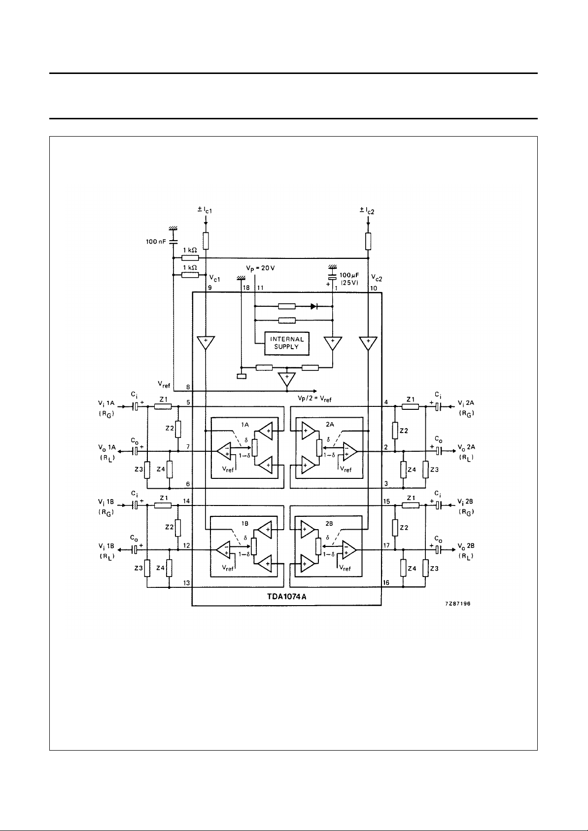
Fig.1 Block diagram and basic external components; Ic1 (at pin 9) and Ic2 (at pin 10) are control input currents;
Vc1 (at pin 9) and Vc2 (at pin 10) are control input voltages with respect to V
Z1 = Z2 = Z3 = Z4 =22 kΩ; the input generator resistance RG = 60 Ω; the output load resistance
RL = 4,7 kΩ; the coupling capacitors at the inputs and outputs are Ci = 2,2 µF and Co = 10 µF
respectively.
December 1982 3
= VP/2 at pin 8;
ref
Philips Semiconductors Product specification
Dual tandem electronic
TDA1074A
potentiometer circuit
RATINGS
Limiting values in accordance with the Absolute Maximum System (IEC 134)
Supply voltage (pin 11) V
Control voltages (pins 9 and 10) ±V
P
; ±V
c1
c2
Input voltage ranges (with respect to pin 18)
at pins 3, 4, 5, 6, 13, 14, 15, 16 V
Total power dissipation P
Storage temperature range T
Operating ambient temperature range T
i
tot
stg
amb
THERMAL RESISTANCE
From crystal to ambient R
th cr-a
REMARK
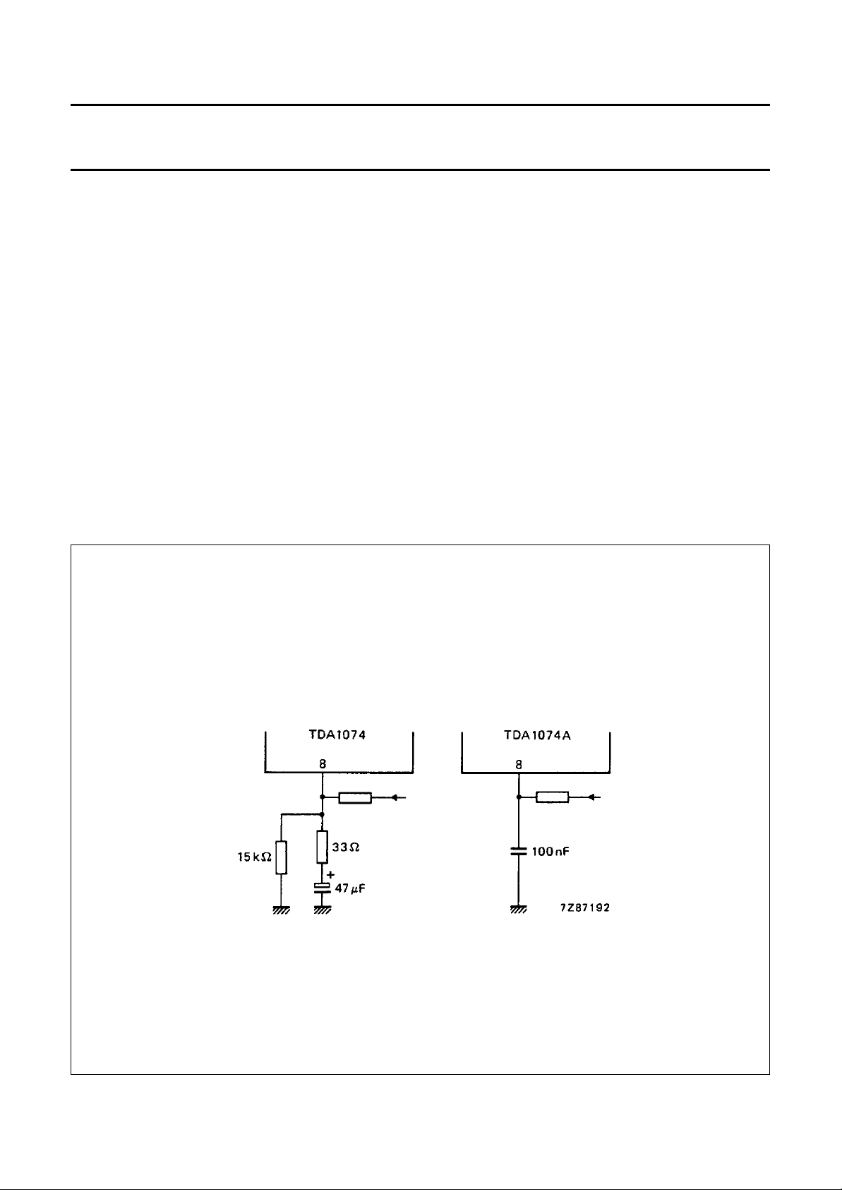
The difference between the TDA1074 and its successor the TDA1074A is shown in Fig.2 as the different component
configuration at pin 8.
max. 23 V
max. 1 V
0 to VPV
max. 800 mW
−55 to + 150 °C
−30 to + 80 °C
= 80 K/W
Fig.2 Component configuration at pin 8 showing the difference between the TDA1074 and the TDA1074A.
December 1982 4

Philips Semiconductors Product specification
Dual tandem electronic
TDA1074A
potentiometer circuit
APPLICATION INFORMATION
Treble and bass control circuit
= 20 V; T
V
P
response (V
Supply current (without load) I
Frequency response (−1 dB)
= Vc2 = 0 V f 10 − 20 000 Hz
V
c1
Voltage gain at linear frequency
response (Vc1 = Vc2 = 0 V) G
Gain variation at f = 1 kHz
at maximum bass/treble boost or
cut at ±V
Bass boost at 40 Hz (ref. 1 kHz)
Vc2 = 120 mV − 17,5 − dB
= 25 °C; measured in Fig.3; RG= 60 Ω; RL> 4,7 kΩ; CL< 30 pF; f = 1 kHz; with a linear frequency
amb
= Vc2= 0 V); unless otherwise specified
c1
PARAMETER SYMBOL MIN. TYP. MAX. UNIT
14 22 30 mA
− 0 − dB
−±1−dB
= ±Vc2 = 120 mV ∆G
c1
P
(1)
v
(1)
v
Bass cut at 40 Hz (ref. 1 kHz)
= 120 mV − 17,5 − dB
−V
c2
Treble boost at 16 kHz (ref. 1 kHz)
= 120 mV − 16 − dB
V
c1
Treble cut at 16 kHz (ref. 1 kHz)
= 120 mV − 16 − dB
−V
c1
Total harmonic distortion
o(rms)
= 300 mV
at V
f = 1 kHz (measured selectively) THD − 0,002 − %
f = 20 Hz to 20 kHz THD − 0,005 − %
at V
o(rms)
= 5 V
f = 1 kHz THD − 0,015 0,1 %
f = 20 Hz to 20 kHz THD − 0,05 0,1 %
Signal level at THD = 0,7%
(input and output) V
i; o(rms)
5,5 6,2 − V
Power bandwidth at reference
level V
= 5 V (−3 dB);
o(rms)
THD = 0,1% B − 40 − kHz
December 1982 5
 Loading...