Philips TDA1029 Datasheet

INTEGRATED CIRCUITS
DATA SH EET
TDA1029
Signal-sources switch
Product specification
File under Integrated Circuits, IC01
January 1980

Philips Semiconductors Product specification
Signal-sources switch TDA1029
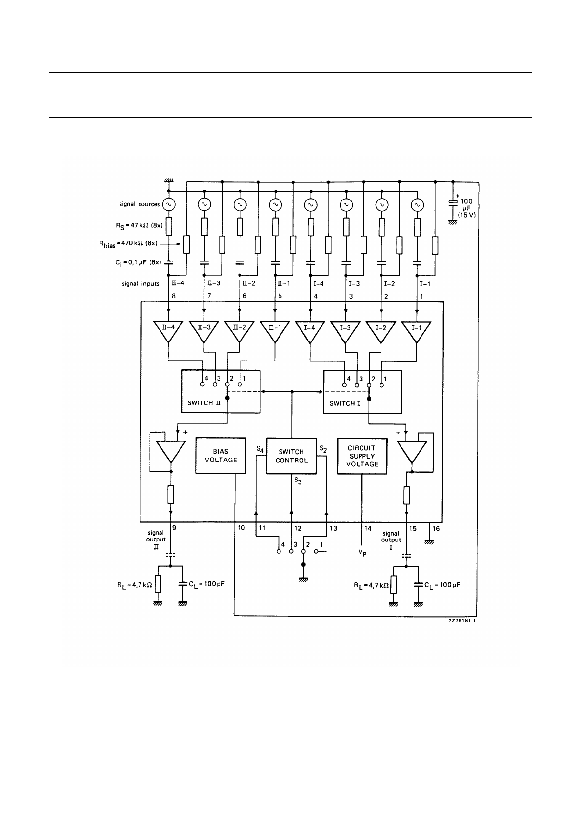
The TDA1029 is a dual operational amplifier (connected as an impedance converter) each amplifier having 4 mutually
switchable inputs which are protected by clamping diodes. The input currents are independent of switch position and the
outputs are short-circuit protected.
The device is intended as an electronic two-channel signal-source switch in a.f. amplifiers.
QUICK REFERENCE DATA
Supply voltage range (pin 14) V
Operating ambient temperature T
Supply voltage (pin 14) V
Current consumption I
Maximum input signal handling (r.m.s. value) V
Voltage gain G
Total harmonic distortion d
P
amb
P
14
i(rms)
v
tot
typ. 20 V
typ. 3,5 mA
typ. 6 V
typ. 1
typ. 0,01 %
6 to 23 V
−30 to + 80 °C
Crosstalk α typ. 70 dB
Signal-to-noise ratio S/N typ. 120 dB
PACKAGE OUTLINE
16-lead DIL; plastic (SOT38); SOT38-1; 1996 July 18.
January 1980 2

Philips Semiconductors Product specification
Signal-sources switch TDA1029
Fig.1 Block diagram.
January 1980 3

Philips Semiconductors Product specification
Signal-sources switch TDA1029
RATINGS
Limiting values in accordance with the Absolute Maximum System (IEC 134)
Supply voltage (pin 14) V
Input voltage (pins 1 to 8) V
Switch control voltage (pins 11, 12 and 13) V
Input current ±I
Switch control current −I
Total power dissipation P
Storage temperature T
Operating ambient temperature T
CHARACTERISTICS
= 20 V; T
V
P
= 25 °C; unless otherwise specified
amb
Current consumption
without load; I
= I15 = 0 2 to 5 mA
9
Supply voltage range (pin 14) V
−V
I
14
P
I
I
S
I
S
tot
stg
amb
P
max. 23 V
max. V
P
max. 0,5 V
0 to 23 V
max. 20 mA
max. 50 mA
max. 800 mW
−55 to + 150 °C
−30 to + 80 °C
typ. 3,5 mA
6 to 23 V
Signal inputs
Input offset voltage
of switched-on inputs
R
≤ 1 kΩ < 10 mV
S
Input offset current
of switched-on inputs < 200 nA
V
io
I
io
typ. 2 mV
typ. 20 nA
Input offset current
of a switched-on input with respect to a
non-switched-on input of a channel < 200 nA
Input bias current
independent of switch position < 950 nA
I
io
I
i
typ. 20 nA
typ. 250 nA
Capacitance between adjacent inputs C typ. 0,5 pF
D.C. input voltage range V
Supply voltage rejection ratio; R
≤ 10 kΩ SVRR typ. 100 µV/V
S
I
3 to 19 V
Equivalent input noise voltage
R
= 0; f = 20 Hz to 20 kHz (r.m.s. value) V
S
n(rms)
typ. 3,5 µV
Equivalent input noise current
f = 20 Hz to 20 kHz (r.m.s. value) I
n(rms)
typ. 0,05 nA
Crosstalk between a switched-on input
and a non-switched-on input;
measured at the output at R
= 1 kΩ; f = 1 kHz α typ. 100 dB
S
January 1980 4

Philips Semiconductors Product specification
Signal-sources switch TDA1029
Signal amplifier
Voltage gain of a switched-on input
= I15 = 0; RL = ∞ G
at I
9
Current gain of a switched-on amplifier G
Signal outputs
v
i
typ. 1
typ. 10
5
Output resistance (pins 9 and 15) R
Output current capability at V
= 6 to 23 V ±I9; ±I
P
o
15
typ. 400 Ω
typ. 5 mA
Frequency limit of the output voltage
V
= 1 V; RS = 1 kΩ; RL = 10 MΩ; CL = 10 pF f typ. 1,3 MHz
i(p-p)
Slew rate (unity gain); ∆V
R
= 10 MΩ; CL = 10 pF S typ. 2 V/µs
L
9-16
/∆t; ∆V
15-16
/∆t
Bias voltage
D.C. output voltage
Output resistance R
V
10-16
10-16
typ. 11 V
10,2 to 11,8 V
typ. 8,2 kΩ
Switch control
switched-on interconnected control voltages
inputs pins V
11-16
V
12-16
I-1, II-1 1-15, 5-9 H H H
I-2, II-2 2-15, 6-9 H H L
I-3, II-3 3-15, 7-9 H L H
I-4, II-4 4-15, 8-9 L H H
I-4, II-4 4-15, 8-9 L L H
I-4, II-4 4-15, 8-9 L H L
I-4, II-4 4-15, 8-9 L L L
I-3, II-3 3-15, 7-9 H L L
V
(1)
13-16
In the case of offset control, an internal blocking circuit of the switch control ensures that not more than one input will be
switched on at a time. In that case safe switching-through is obtained at V
≤ 1,5 V.
SL
January 1980 5
 Loading...