


DATA SH EET
Product specification
Supersedes data of August 1982
File under Integrated Circuits, IC02
May 1991
INTEGRATED CIRCUITS
TDA1023/T
Proportional-control triac triggering
circuit

May 1991 2
Philips Semiconductors Product specification
Proportional-control triac triggering circuit TDA1023/T
FEATURES
• Adjustable width of proportional range
• Adjustable hysteresis
• Adjustable width of trigger pulse
• Adjustable repetition timing of firing burst
• Control range translation facility
• Fail safe operation
• Supplied from the mains
• Provides supply for external temperature bridge
APPLICATIONS
• Panel heaters
• Temperature control
GENERAL DESCRIPTION
The TDA1023 is a bipolar integrated circuit for controlling
triacs in a proportional time or burst firing mode. Permitting
precise temperature control of heating equipment it is
especially suited to the control of panel heaters.
It generates positive-going trigger pulses but complies with
regulations regarding mains waveform distortion and RF
interference.
QUICK REFERENCE DATA
Note
1. Negative current is defined as conventional current flow out of a device. A negative output current is suited for
positive triac triggering.
ORDERING INFORMATION
Note
1. TDA1023: 16 DIL; plastic (SOT38); SOT38-1; 1996 November 27.
2. TDA1023T: 16 mini-pack; plastic (SO16; SOT109A); SOT109-1; 1996 November 27.
SYMBOL PARAMETER MIN. TYP. MAX. UNIT
V
CC
supply voltage (derived from mains voltage) − 13.7 − V
V
Z
stabilized supply voltage for temperature bridge − 8 − V
I
16(AV)
supply current (average value) − 10 − mA
t
w
trigger pulse width − 200 −µs
T
b
firing burst repetition time at CT = 68 µF − 41 − s
-I
OH
(1)
output current −−150 mA
T
amb
operating ambient temperature range −20 − +75 °C
EXTENDED
TYPE NUMBER
PACKAGE
PINS PIN POSITION MATERIAL CODE
TDA1023 16 DIL plastic SOT38
(1)
TDA1023T 16 mini-pack plastic SO16; SOT109A
(2)
May 1991 3
Philips Semiconductors Product specification
Proportional-control triac triggering circuit TDA1023/T
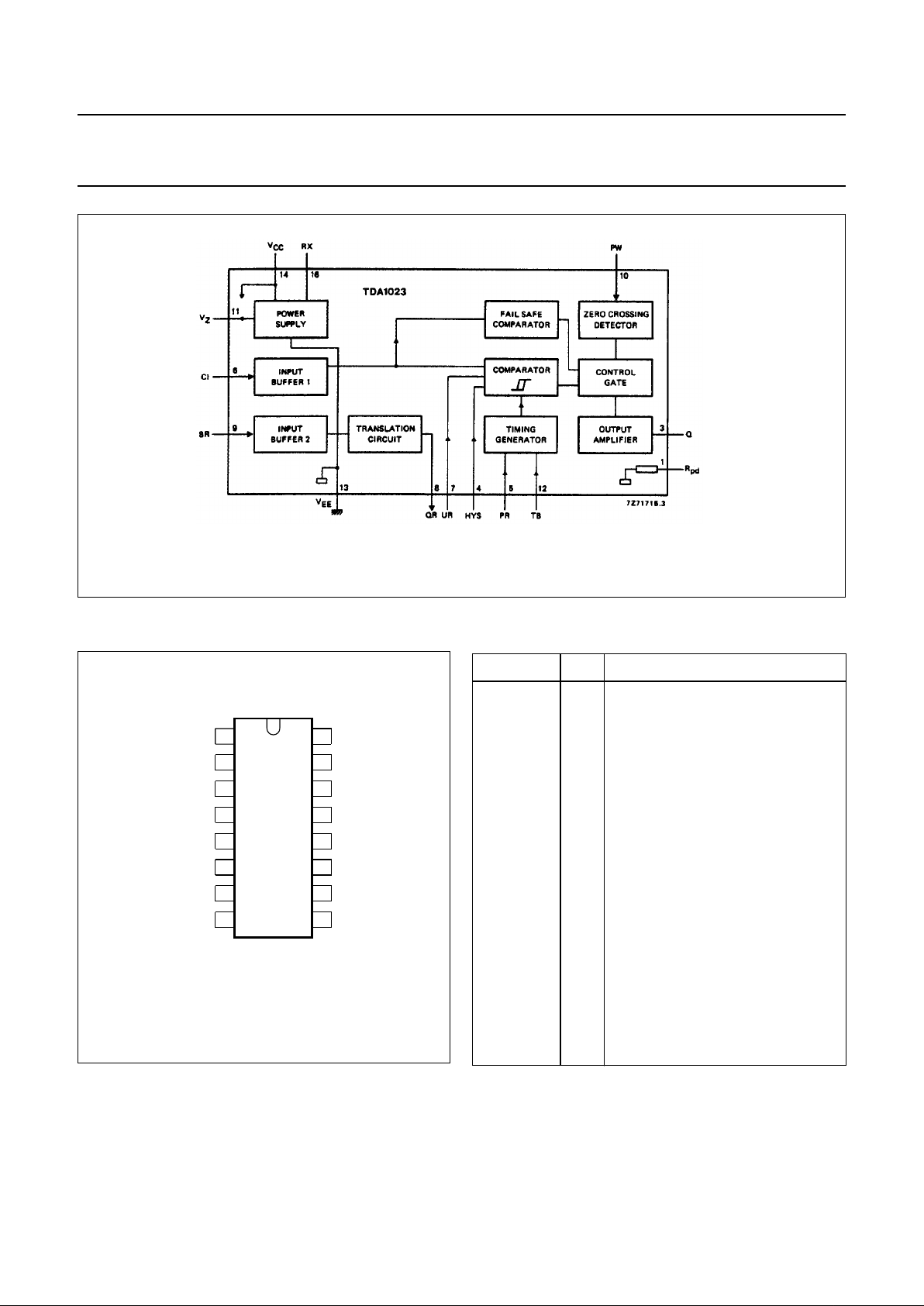
Fig.1 Block diagram.
handbook, halfpage
1
2
3
4
5
6
7
8
16
15
14
13
12
11
10
9
TDA1023
R
pd
n.c.
Q
HYS
PR
CI
UR
QR
BR
PW
TB
V
EE
V
Z
V
CC
n.c.
RX
MBA484
Fig.2 Pin configuration.
PINNING
SYMBOL PIN DESCRIPTION
R
pd
1 internal pull-down resistor
n.c. 2 not connected
Q 3 output
HYS 4 hysteresis control input
PR 5 proportional range control input
CI 6 control input
UR 7 unbuffered reference input
QR 8 output of reference buffer
BR 9 buffered reference input
PW 10 pulse width control input
V
Z
11 reference supply output
TB 12 firing burst repetition time control
input
V
EE
13 ground
V
CC
14 positive supply
n.c. 15 not connected
RX 16 external resistor connection

May 1991 4
Philips Semiconductors Product specification
Proportional-control triac triggering circuit TDA1023/T
FUNCTIONAL DESCRIPTION
The TDA1023 generates pulses to trigger a triac. These
pulses coincide with the zero excursions of the mains
voltage, thus minimizing RF interference and mains supply
transients. In order to gate the load on and off, the trigger
pulses occur in bursts thus further reducing mains supply
pollution. The average power in the load is varied by
modifying the duration of the trigger pulse burst in
accordance with the voltage difference between the
control input CI and the reference input, either UR or BR.
Power supply: V
CC
, RX and Vz (pins 14, 16 and 11)
The TDA1023 is supplied from the AC mains via a resistor
R
D
to the RX connection (pin 16); the VEE connection (pin
13) is linked to the neutral line (see Fig.4a). A smoothing
capacitor CS should be coupled between the VCC and V
EE
connections.
A rectifier diode is included between the RX and V
CC
connections whilst the DC supply voltage is limited by a
chain of stabilizer diodes between the RX and V
EE
connections (see Fig.3).
A stabilized reference voltage (VZ) is available at pin 11 to
power an external temperature sensing bridge.
Supply operation
During the positive mains half-cycles the current through
the external voltage dropping resistor R
D
charges the
external smoothing capacitor CS until RX attains the
stabilizing potential of the internal stabilizing diodes. R
D
should be selected to be capable of supplying the current
ICC for the TDA1023, the average output current I
3(AV)
,
recharge the smoothing capacitor CS and provide the
supply for an external temperature bridge. (see Figs 9 to
12). Any excess current is by-passed by the internal
stabilizer diodes. The maximum rated supply current,
however, must not be exceeded.
During the negative mains half-cycles external smoothing
capacitor CS supplies the sum of the current demand
described above. Its capacitance must be sufficiently high
to maintain the supply voltage above the specified
minimum.
Dissipation in resistor RD is halved by connecting a diode
in series (see Fig.4b and 9 to 12). A further reduction in
dissipation is possible by using a high quality dropping
capacitor CD in series with a resistor RSD (see Figs 4c and
14). Protection of the TDA1023 and the triac against
mains-borne transients can be provided by connecting a
suitable VDR across the mains input.
Control and reference inputs CI, BR and UR
(pins 6, 9 and 7)
For the control of room temperature (5 °C to 30 °C)
optimum performance is obtained by using the translation
circuit. The buffered reference input BR (pin 9) is used as
a reference input whilst the output reference buffer QR (pin
8) is connected to the unbuffered reference input UR
(pin 7). This ensures that the range of room temperature is
encompassed in most of the rotation of the potentiometer
to give a linear temperature scale with accurate setting.
Should the translation circuit not be required, the
unbuffered reference input UR (pin 7) is used as a
reference input. The buffered reference input BR (pin 9)
must then be connected to the reference supply output V
Z
(pin 11).
For proportional power control the unbuffered reference
input UR (pin 7) must be connected to the firing burst
repetition time control input TB (pin 12).The buffered
reference input BR (pin 9), which is in this instance
inactive, must then be connected to the reference supply
output VZ (pin 11).
Proportional range control input PR (pin 5)
The output duty factor changes from 0% to 100% by a
variation of 80 mV at the control input CI (pin 6) with the
proportional range control input PR open. For temperature
control this corresponds to a temperature difference of 1 K.
By connecting the proportional range control input PR
(pin 5) to ground the range may be increased to 400 mV,
i.e. 5 K. Intermediate values may be obtained by
connecting the PR input to ground via a resistor R5
(see Table 1).
Hysteresis control input HYS (pin 4)
With the hysteresis control input HYS (pin 4) open, the
device has a built-in hysteresis of 20 mV. For temperature
control this corresponds with 0.25 K.
Hysteresis is increased to 320 mV, corresponding to 4 K,
by grounding HYS (pin 4). Intermediate values are
obtained by connecting pin 4 via resistor R4 to ground.
Table 1 provides a set of values for R4 and R5 giving a
fixed ratio between hysteresis and proportional range.

May 1991 5
Philips Semiconductors Product specification
Proportional-control triac triggering circuit TDA1023/T
Trigger pulse width control input PW (pin 10)
The width of the trigger pulse may be adjusted to the value
required for the triac by choosing the value of the external
synchronization resistor RS between the trigger pulse
width control input PW (pin 10) and the AC mains.
The pulse width is inversely proportional to the input
current (see Fig.13).
Output Q (pin 3)
Since the circuit has an open-emitter output it is capable of
sourcing current. It is thus suited for generating
positive-going trigger pulses. The output is current-limited
and short-circuit protected. The maximum output current is
150 mA and the output pulses are stabilized at 10 V for
output currents up to that value.
To minimize the total supply current and power dissipation,
a gate resistor R
G
must be connected between the output
Q and the triac gate to limit the output current to the
minimum required by the triac (see Figs 5 to 8).
Pull-down resistor R
pd
(pin 1)
The TDA1023 includes a 1.75 kΩ pull-down resistor R
pd
between pins 1 and 13 (VEE, ground connection) intended
for use with sensitive triacs.
LIMITING VALUES
In accordance with the Absolute Maximum System (IEC 134)
SYMBOL PARAMETER MIN. MAX. UNIT
V
CC
DC supply voltage − 16 V
Supply current
I
16(AV)
average − 30 mA
I
16(RM)
repetitive peak − 100 mA
I
16(SM)
non-repetitive peak (tp < 50 µs) − 2A
V
I
input voltage, all inputs − 16 V
I
6, 7, 9, 10
input current − 10 mA
V
1
voltage on Rpd connection − 16 V
V
3, 8, 11
output voltage, Q, QR, V
Z
− 16 V
Output current
-I
OH(AV)
average − 30 mA
-I
OH(M)
peak max. 300 µs − 700 mA
P
tot
total power dissipation − 500 mW
T
stg
storage temperature range −55 +150 °C
T
amb
operating ambient temperature range −20 +75 °C
May 1991 6
Philips Semiconductors Product specification
Proportional-control triac triggering circuit TDA1023/T
CHARACTERISTICS
VCC = 11 to 16 V; T
amb
= −20 to +75 °C unless otherwise specified
SYMBOL PARAMETER CONDITIONS MIN. TYP. MAX. UNIT
Supply
V
CC
internally stabilized supply voltage at
I16 = 10 mA
12 13.7 15 V
∆V
CC
/∆I16variation with I
16
− 30 − mV/mA
I
16
supply current at V
16-13
= 11 to 16 V;
I10 = 1mA; f = 50 Hz; pin 11 open;
V
6-13
> V
7-13
pins 4 and 5 open −−6mA
pins 4 and 5 grounded −−7.1 mA
Reference supply output V
Z
(pin 11) for external temperature bridge
V
11-13
output voltage − 8 − V
−I
11
output current −−1mA
Control and reference inputs CI, BR and UR (pins 6, 9 and 7)
V
6-13
input voltage to inhibit the output − 7.6 − V
I
6, 7, 9
input current V1 = 4 V −−2 µA
Hysteresis control input HYS (pin 4)
∆V
6
hysteresis pin 4 open 9 20 40 mV
∆V
6
hysteresis pin 4 grounded − 320 − mV
Proportional control range input PR (pin 5)
∆V
6
proportional range pin 5 open 50 80 130 mV
∆V
6
proportional range pin 5 grounded − 400 − mV
Pulse width control input PW (pin 10)
t
w
pulse width I
10(RMS)
= 1mA; f = 50 Hz 100 200 300 µs
Firing burst repetition time control input TB (pin 12)
TbC
T
firing burst repetition time, ratio to
capacitor C
T
320 600 960 ms/µF
Output of reference buffer QR (pin 8)
output voltage at input voltage:
V
8-13
V
9-13
= 1.6 V − 3.2 − V
V
8-13
V
9-13
= 4.8 V − 4.8 − V
V
8-13
V
9-13
= 8 V − 6.4 − V
Output Q (pin 3)
V
OH
output voltage HIGH −IOH = 150 mA 10 −−V
−I
OH
output current HIGH −−150 mA
Internal pull-down resistor R
pd
(pin 1)
R
pd
resistance to V
EE
1 1.75 3 kΩ
 Loading...