Philips TDA1020-N4-S5, TDA1020-N4 Datasheet

DATA SH EET
Product specification
File under Integrated Circuits, IC01
November 1982
INTEGRATED CIRCUITS
TDA1020
12 W car radio power amplifier

November 1982 2 Preliminary Specification
Philips Semiconductors Product specification
12 W car radio power amplifier TDA1020
The TDA1020 is a monolithic integrated 12 W audio amplifier in a 9-lead single in-line (SIL) plastic package. The device
is primarily developed as a car radio amplifier. At a supply voltage of VP= 14,4 V, an output power of 7 W can be delivered
into a 4 Ω load and 12 W into 2 Ω.
To avoid interferences and car ignition signals coming from the supply lines into the IC, frequency limiting is used beyond
the audio spectrum in the preamplifier and the power amplifier.
The maximum supply voltage of 18 V makes the IC also suitable for mains-fed radio receivers, tape recorders or record
players. However, if the supply voltage is increased above 18 V (< 45 V), the device will not be damaged (load dump
protected). Also a short-circuiting of the output to ground (a.c.) will not destroy the device. Thermal protection is built-in.
As a special feature, the circuit has a low stand-by current possibility.
The TDA1020 is pin-to-pin compatible with the TDA1010.
QUICK REFERENCE DATA
PACKAGE OUTLINE
9-lead SIL; plastic (SOT110B); SOT110-1; 1996 July 24.
Supply voltage range V
P
6 to 18 V
Repetitive peak output current I
ORM
<4A
Output power at d
tot
= 10% (with bootstrap)
V
P
= 14,4 V; RL = 2 Ω P
o
>10W
typ. 12 W
V
P
= 14,4 V; RL = 4 Ω P
o
typ. 7 W
V
P
= 14,4 V; RL = 8 Ω P
o
typ. 3,5 W
Output power at d
tot
= 10% (without bootstrap)
V
P
= 14,4 V; RL = 4 Ω P
o
> 4,5 W
Input impedance
preamplifier (pin 8) |Z
i
| typ. 40 kΩ
power amplifier (pin 6) |Z
i
| typ. 40 kΩ
Total quiescent current at V
P
= 14,4 V I
tot
typ. 30 mA
Stand-by current I
sb
<1mA
Storage temperature range T
stg
−55 to + 150 °C
Crystal temperature T
c
max. 150 °C

November 1982 3 Preliminary Specification
Philips Semiconductors Product specification
12 W car radio power amplifier TDA1020
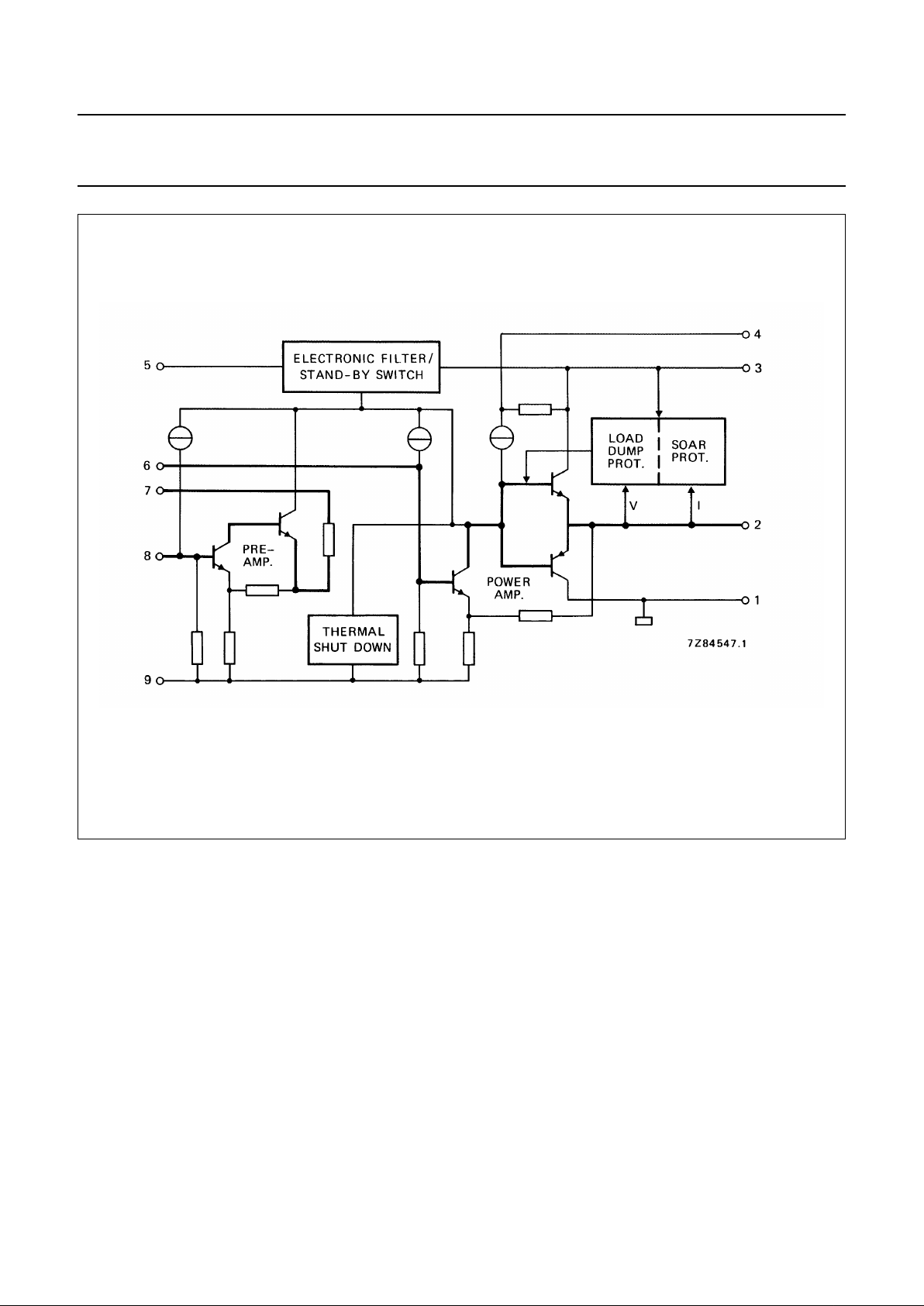
PINNING
1. Negative supply (substrate)
2. Output power stage
3. Positive supply (VP)
4. Bootstrap
5. Ripple rejection filter
6. Input power stage
7. Output preamplifier
8. Input preamplifier
9. Negative supply
Fig.1 Internal block diagram; the heavy lines indicate the signal paths.
 Loading...