


DATA SH EET
Product specification
File under Integrated Circuits, IC01
July 1994
INTEGRATED CIRCUITS
TDA1013B
4 W audio power amplifier with
DC volume control

July 1994 2
Philips Semiconductors Product specification
4 W audio power amplifier with
DC volume control
TDA1013B
GENERAL DESCRIPTION
The TDA1013B is an integrated audio amplifier circuit with DC volume control, encapsulated in a 9-lead single in-line
(SIL) plastic package. The wide supply voltage range makes this circuit ideal for applications in mains and battery-fed
apparatus such as television receivers and record players.
The DC volume control stage has a logarithmic control characteristic with a range of more than 80 dB; control is by means
of a DC voltage variable between 2 and 6.5 V.
The audio amplifier has a well defined open loop gain and a fixed integrated closed loop. This device requires only a few
external components and offers stability and performance.
Features
• Few external components
• Wide supply voltage range
• Wide control range
• Pin compatible with TDA1013A
• Fixed gain
• High signal-to-noise ratio
• Thermal protection
QUICK REFERENCE DATA
PACKAGE OUTLINE
9-lead SIL; plastic (SOT110B); SOT110-1; 1996 July 23.
PARAMETER CONDITIONS SYMBOL MIN. TYP. MAX. UNIT
Supply voltage V
P
10 18 40 V
Repetitive peak output
current I
ORM
−−1.5 A
Total sensitivity P
o
= 2.5 W;
DC control at max. gain V
i
44 55 69 mV
Audio amplifier
Output power THD = 10%; RL = 8 Ω P
o
4.0 4.2 − W
Total harmonic distortion P
o
= 2.5 W; RL = 8 Ω THD − 0.15 0.1 %
Sensitivity P
o
= 2.5 W V
i
100 125 160 mV
DC volume control unit
Gain control range |∆Gv|80−−dB
Signal handling THD < 1%;
DC control = 0 dB V
i
1.2 1.7 − V
Sensitivity (pin 6) V
o
= 125 mV;
max. voltage gain V
i
39 45 55 mV
Input impedance (pin 8) |Z
i
| 232935kΩ

July 1994 3
Philips Semiconductors Product specification
4 W audio power amplifier with
DC volume control
TDA1013B
PINNING
1. power ground
2. amplifier output
3. supply voltage
4. electronic filter
5. amplifier input
6. control unit output
7. control voltage
8. control unit input
9. signal ground (substrate)
Fig.1 Block diagram.
July 1994 4
Philips Semiconductors Product specification
4 W audio power amplifier with
DC volume control
TDA1013B
RATINGS
Limiting values in accordance with the Absolute Maximum System (IEC 134)
HEATSINK DESIGN EXAMPLE
Assume V
P
= 18 V; RL = 8 Ω; T
amb
= 60 °C; Tc = 150 °C (max.); for a 4 W application, the maximum dissipation is
approximately 2.5 W. The thermal resistance from junction to ambient can be expressed as:
R
th j-a
= R
th j-tab
+ R
th tab-h
+ R
th h-a =
Since R
th j-tab
= 9 K/W and R
th tab-h
= 1 K/W, R
th h-a
= 36 − (9 + 1) = 26 K/W.
SYMBOL PARAMETER MIN. MAX. UNIT
V
P
Supply voltage − 40 V
I
OSM
Non-repetitive peak output current − 3A
I
ORM
Repetitive peak output current − 1.5 A
T
stg
Storage temperature range −55 +150 °C
T
c
Crystal temperature − +150 °C
P
tot
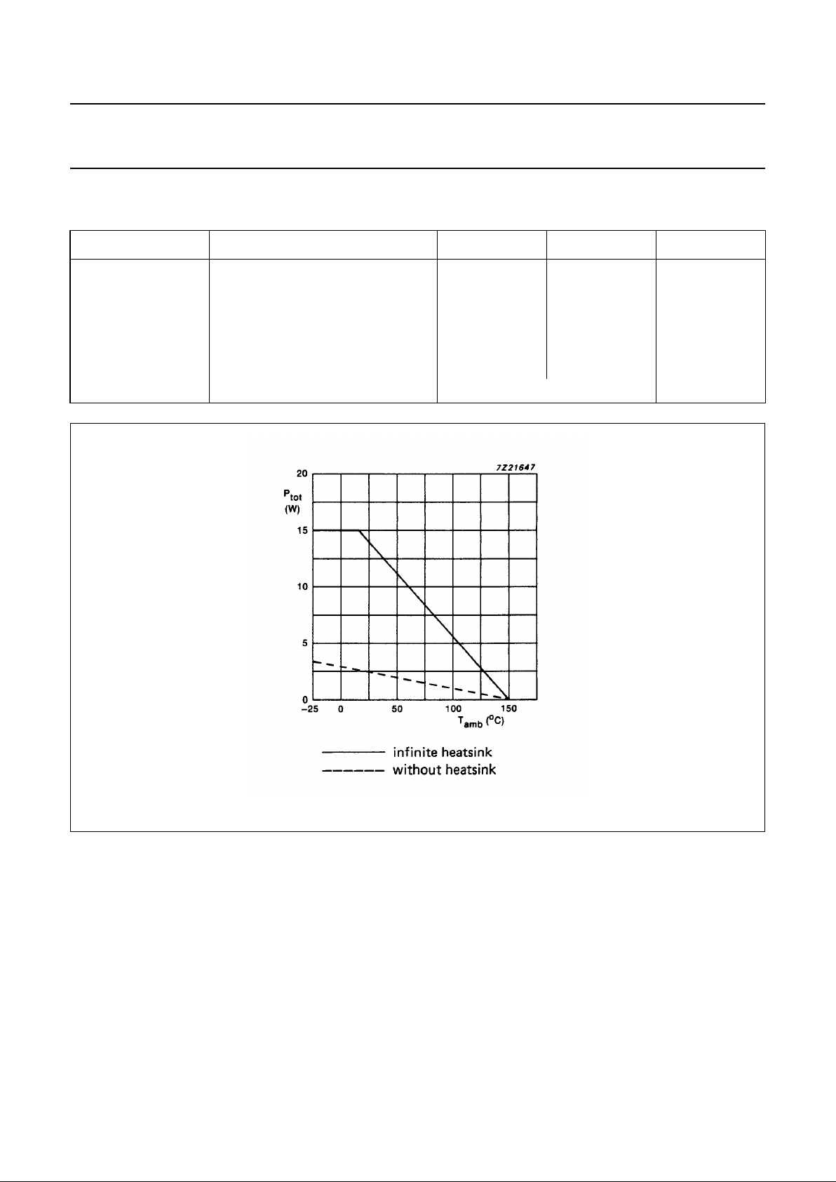
Total power dissipation see Fig.2
Fig.2 Power derating curve.
T
jmaxTamb max
–
P
max
------------------------------------------ -
150 60–
2.5
----------------------
36 K/W==
 Loading...