

Philips TDA1010A Datasheet

INTEGRATED CIRCUITS
DATA SH EET
TDA1010A
6 W audio power amplifier in car
applications
10 W audio power amplifier in
mains-fed applications
Product specification
File under Integrated Circuits, IC01
November 1982

Philips Semiconductors Product specification
6 W audio power amplifier in car applications
10 W audio power amplifier in mains-fed
The TDA1010A is a monolithic integrated class-B audio amplifier circuit in a 9-lead single in-line (SIL) plastic package.
The device is primarily developed as a 6 W car radio amplifier for use with 4 Ωand 2Ωload impedances. The wide supply
voltage range and the flexibility of the IC make it an attractive proposition for record players and tape recorders with
output powers up to 10 W.
Special features are:
• single in-line (SIL) construction for easy mounting
• separated preamplifier and power amplifier
• high output power
• low-cost external components
• good ripple rejection
• thermal protection
QUICK REFERENCE DATA
TDA1010A
Supply voltage range V
Repetitive peak output current I
Output power at pin 2; d
= 14,4 V; RL= 2 Ω P
V
P
V
= 14,4 V; RL= 4 Ω P
P
V
= 14,4 V; RL= 8 Ω P
P
V
= 14,4 V; RL= 2 Ω; with additional bootstrap resistor of 220 Ω between
P
tot
= 10%
pins 3 and 4 P
Total harmonic distortion at P
= 1 W; RL= 4 Ω d
o
P
ORM
o
o
o
o
tot
max. 3 A
typ. 6,4 W
typ. 6,2 W
typ. 3,4 W
typ. 9 W
typ. 0,2 %
6 to 24 V
Input impedance
preamplifier (pin 8) Zi typ. 30 kΩ
power amplifier (pin 6) Z
Total quiescent current at V
Sensitivity for P
= 5,8 W; RL= 4 Ω V
o
= 14,4 V I
P
Operating ambient temperature T
Storage temperature T
typ. 20 kΩ
i
tot
i
amb
stg
typ. 31 mA
typ. 10 mV
−25 to + 150 °C
−55 to + 150 °C
PACKAGE OUTLINE
9-lead SIL; plastic (SOT110B); SOT110-1; 1996 Sepetember 06.
November 1982 2
Philips Semiconductors Product specification
6 W audio power amplifier in car applications
10 W audio power amplifier in mains-fed applications
TDA1010A
November 1982 3
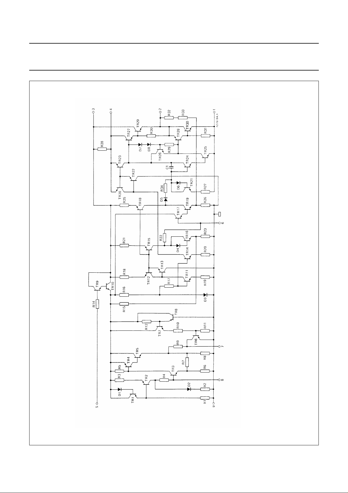
Fig.1 Circuit diagram.
Philips Semiconductors Product specification
6 W audio power amplifier in car applications
TDA1010A
10 W audio power amplifier in mains-fed applications
RATINGS
Limiting values in accordance with the Absolute Maximum System (IEC 134)
Supply voltage V
Peak output current I
Repetitive peak output current I
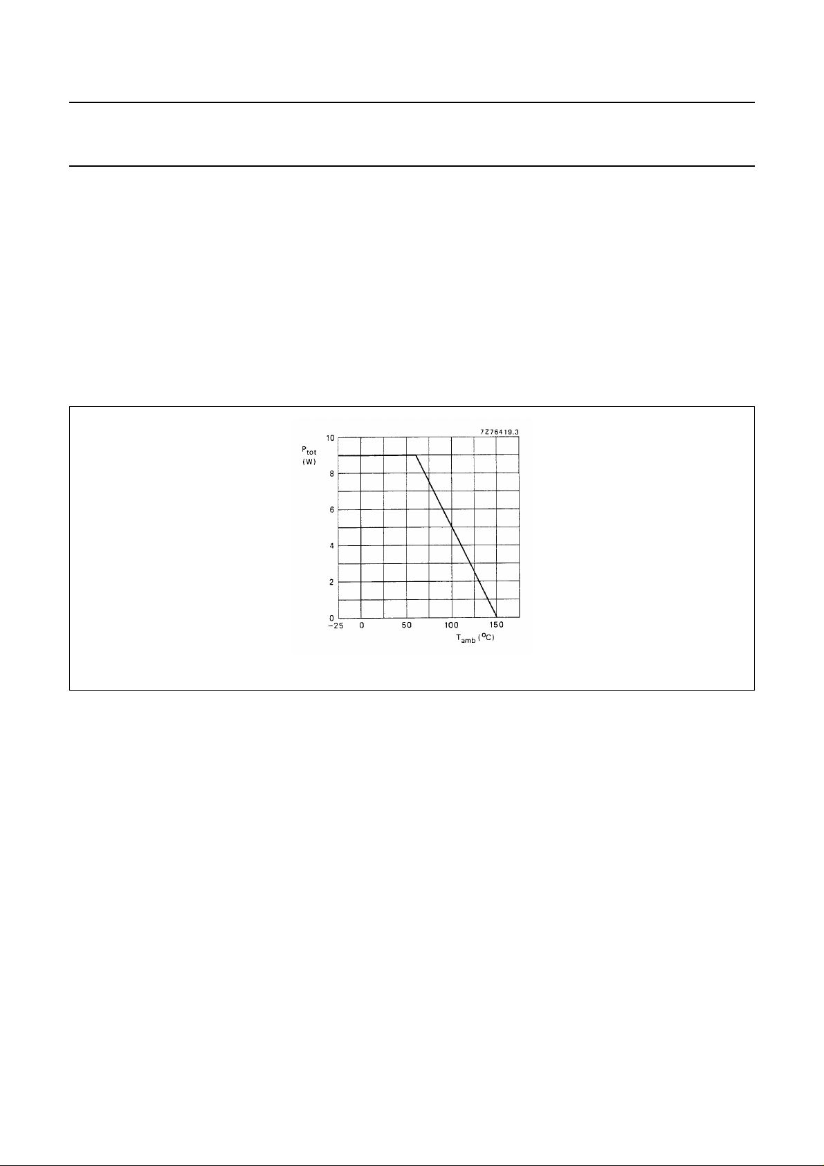
Total power dissipation see derating curve Fig.2
Storage temperature T
Operating ambient temperature T
A.C. short-circuit duration of load during sine-wave drive; without heatsink at
V
= 14,4 V
P
max. 24 V
P
max. 5 A
OM
max. 3 A
ORM
−55 to +150 °C
stg
−25 to +150 °C
amb
t
max. 100 hours
sc
Fig.2 Power derating curve.
HEATSINK DESIGN
Assume V
= 14,4 V; RL= 2 Ω; T
P
= 60 °C maximum; thermal shut-down starts at Tj= 150 °C. The maximum sine-wave
amb
dissipation in a 2 Ω load is about 5,2 W. The maximum dissipation for music drive will be about 75% of the worst-case
sine-wave dissipation, so this will be 3,9 W. Consequently, the total resistance from junction to ambient
R
= R
th j-aRth j-tab
Since R
R
th j-tab
= 23 − (10 + 1) = 12 K/W.
th h-a
++
= 10 K/W and R
th tab-hRth h-a
th tab-h
150 60–
---------------------39,
= 1 K/W,
23 K/W==
.
November 1982 4

Philips Semiconductors Product specification
6 W audio power amplifier in car applications
TDA1010A
10 W audio power amplifier in mains-fed applications
D.C. CHARACTERISTICS
Supply voltage range V
Repetitive peak output current I
Total quiescent current at V
= 14,4 V I
P
P
ORM
tot
A.C. CHARACTERISTICS
T
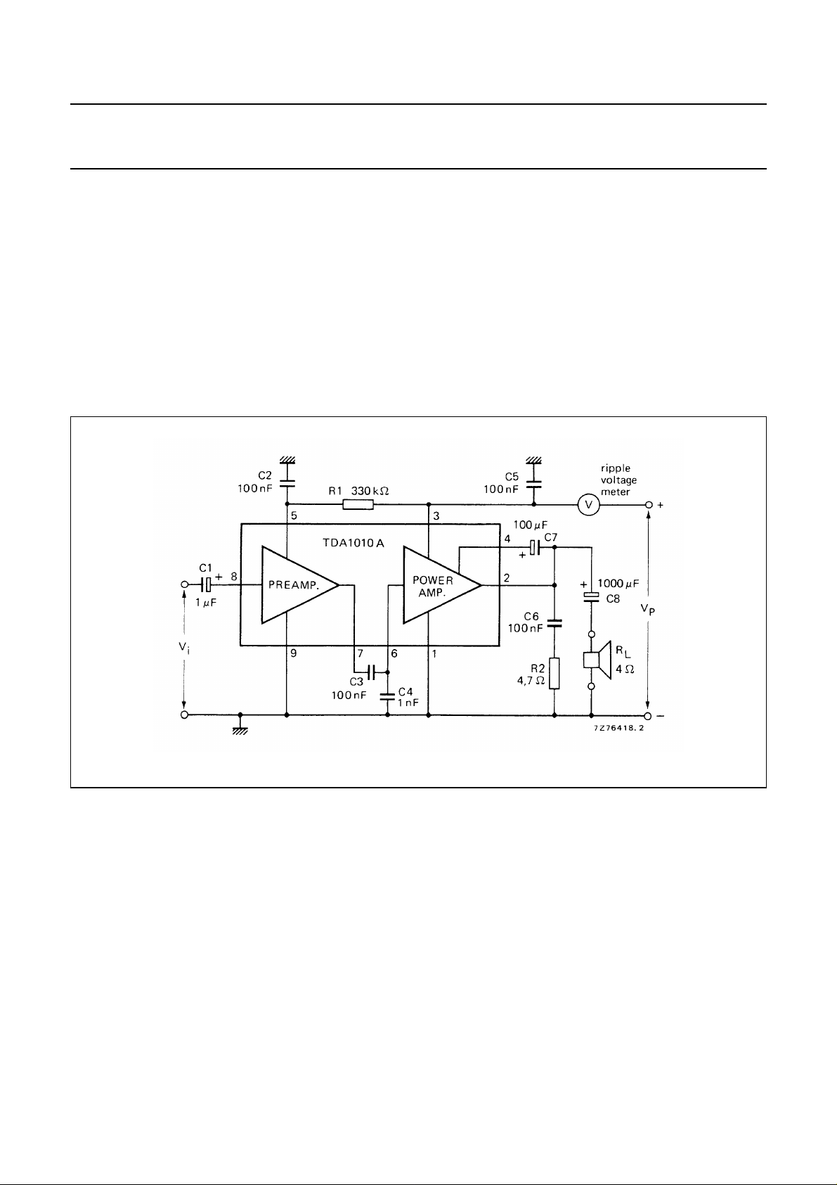
= 25 °C; VP= 14,4 V; RL= 4 Ω; f = 1 kHz unless otherwise specified; see also Fig.3.
amb
A.F. output power (see Fig.4) at d
= 10%;
tot
measured at pin 2; with bootstrap
V
= 14,4 V; RL= 2 Ω (note 1) P
P
V
= 14,4 V; RL= 4 Ω (note 1 and 2)
P
V
= 14,4 V; RL= 8 Ω (note 1) P
P
V
= 14,4 V; RL= 4 Ω; without bootstrap P
P
V
= 14,4 V; RL= 2Ω; with additional bootstrapresistor of 220Ωbetween pins 3 and 4 P
P
o
P
o
o
o
o
Voltage gain
preamplifier (note 3) G
power amplifier G
total amplifier G
Total harmonic distortion at Po= 1 W d
Efficiency at P
= 6 W η typ. 75 %
o
v1
v2
v tot
tot
Frequency response (−3 dB) B 80 Hz to 15 kHz
Input impedance
preamplifier (note 4) Z
typ. 30 kΩ
i
power amplifier (note 5) Zi typ. 20 kΩ
Output impedance of preamplifier; pin 7 (note 5) Zo typ. 20 kΩ
Output voltage preamplifier (r.m.s. value)
d
< 1% (pin 7) (note 3) V
tot
o(rms)
Noise output voltage (r.m.s. value; note 6)
R
= 0 Ω V
S
R
= 8,2 kΩ V
S
n(rms)
n(rms)
Ripple rejection at f = 1 kHz to 10 kHz (note 7) RR > 42 dB
at f = 100 Hz; C2 = 1 µF RR > 37 dB
Sensitivity for Po= 5,8 W V
Bootstrap current at onset of clipping; pin 4 (r.m.s. value) I
i
4(rms)
6 to 24 V
<3A
typ. 31 mA
typ. 6,4 W
> 5,9 W
typ. 6,2 W
typ. 3,4 W
typ. 5,7 W
typ. 9 W
typ. 24 dB
21 to 27 dB
typ. 30 dB
27 to 33 dB
typ. 54 dB
51 to 57 dB
typ. 0,2 %
20 to 40 kΩ
14 to 26 kΩ
14 to 26 kΩ
> 0,7 V
typ. 0,3 mV
typ. 0,7 mV
< 1,4 mV
typ. 10 mV
typ. 30 mA
November 1982 5
Philips Semiconductors Product specification
6 W audio power amplifier in car applications
TDA1010A
10 W audio power amplifier in mains-fed applications
Notes
1. Measured with an ideal coupling capacitor to the speaker load.
2. Up to Po≤ 3 W : d
3. Measured with a load impedance of 20 kΩ.
4. Independent of load impedance of preamplifier.
5. Output impedance of preamplifier (ZΟ) is correlated (within 10%) with the input impedance (Zi) of the power
amplifier.
6. Unweighted r.m.s. noise voltage measured at a bandwidth of 60 Hz to 15 kHz (12 dB/octave).
7. Ripple rejection measured with a source impedance between 0 and 2 kΩ (maximum ripple amplitude: 2 V).
8. The tab must be electrically floating or connected to the substrate (pin 9).
tot
≤ 1%.
Fig.3 Test circuit.
November 1982 6
Philips Semiconductors Product specification
6 W audio power amplifier in car applications
10 W audio power amplifier in mains-fed applications
TDA1010A
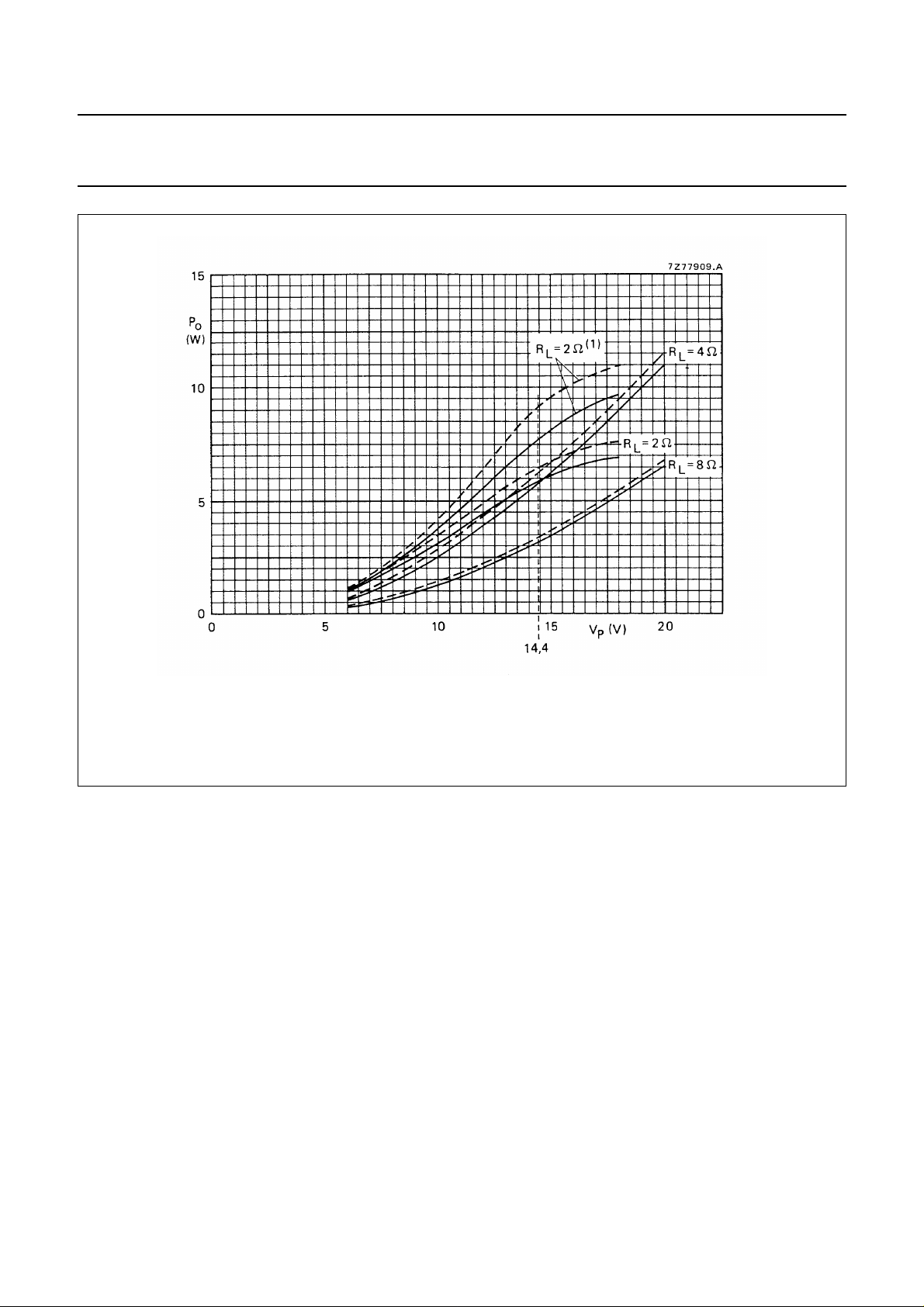
Fig.4 Output power of the circuit of Fig.3 as a function of the supply voltage with the load impedance as a
parameter; typical values. Solid lines indicate the power across the load, dashed lines that available at pin
2 of the TDA1010. RL= 2 Ω
pins 3 and 4. Measurements were made at f = 1 kHz, d
Fig. 5 See next page.
Total harmonic distortion in the circuit of Fig.3 as a function of the output power with the load impedance as a parameter;
typical values. Solid lines indicate the power across the load, dashed lines that available at pin 2 of the TDA1010.
RL= 2 Ω
made at f = 1 kHz, VP= 14,4 V.
(1)
has been measured with an additional 220 Ω bootstrap resistor between pins 3 and 4. Measurements were
(1)
has been measured with an additional 220 Ω bootstrap resistor between
= 10%, T
tot
amb
= 25 °C.
November 1982 7
 Loading...