

Philips TDA10085HT Datasheet
INTEGRATED CIRCUITS
DATA SH EET
TDA10085HT
Single chip DVB-S/DSS channel
receiver
Product specification
Supersedes data of 2000 March 16
File under Integrated Circuits, IC02
2001 Aug 31

Philips Semiconductors Product specification
Single chip DVB-S/DSS channel receiver TDA10085HT
CONTENTS
11 FEATURES
2 APPLICATIONS
3 GENERAL DESCRIPTION
4 ORDERING INFORMATION
5 BLOCK DIAGRAM
6 PINNING
7 LIMITING VALUES
8 THERMAL CHARACTERISTICS
9 CHARACTERISTICS
10 APPLICATION INFORMATION
11 PACKAGE OUTLINE
12 SOLDERING
12.1 Introduction to soldering surface mount
packages
12.2 Reflow soldering
12.3 Wave soldering
12.4 Manual soldering
12.5 Suitability of surface mount IC packages for
wave and reflow soldering methods
13 DATA SHEET STATUS
14 DEFINITIONS
15 DISCLAIMERS
16 PURCHASE OF PHILIPS I2C COMPONENTS
2001 Aug 31 2

Philips Semiconductors Product specification
Single chip DVB-S/DSS channel receiver TDA10085HT
1 FEATURES
• DSS andDVB-S compliant single chip demodulator and
forward error correction
• Dual 6-bit Analog-to-Digital Converter (ADC) on-chip
• PLL that allows using a low-cost crystal
(typically 4 MHz)
• DiSEqC 1.X from 1 to 8 byte-long sequences with
modulated or unmodulated output
• DSS dish control
• Digital cancellation of ADC offset
• Simultaneous parallel and serial output interfaces
• Variable rate BPSK/QPSK coherent demodulator
• Modulation rate variable from 1 to 49 Mbauds
• Automatic gain control output
• Digital symbol timing recovery:
– Acquisition range up to 960 ppm
• Carrier offset cancellation upto onehalf of the sampling
frequency
• Digital carrier recovery:
– Acquisition range up to 12% of the symbol rate
• Half-Nyquist filters: roll-off = 0.35 for DVB and
0.2 for DSS
• Interpolating and anti-aliasing filters to handle variable
symbol rates
• Channel quality estimation
• Spectral inversion ambiguity resolution
• Viterbi decoder:
– Supported rates from 1/2 to 8/9
– Constraint length K = 7 with G1 = 1718 and
G2 = 133
– Viterbi output BER measurement
– Automatic code rate search within1/2,2/3 and6/7 in
DSS mode
– Automatic code rate search within1/2,2/3,3/4,5/
and7/8 in DVB-S mode
• Convolutional de-interleaver and Reed Solomon
decoder according to DVB and DSS specifications
• Automatic frame synchronization
• Selectable DVB-S descrambling
• I2C-bus interface
• 64-pin TQFP package
• CMOS technology (0.2 µm, 1.8 V to 3.3 V).
8
6
2 APPLICATIONS
• DVB-S receivers (ETS 300-421)
• DSS receivers.
3 GENERAL DESCRIPTION
The TDA10085 is a single-chip channel receiver for
satellite television reception matching both DSS and
DVB-S standards. The device contains a dual 6-bit flash
ADC, variable rate BPSK/QPSK coherent demodulator
andforward error correctionfunctions.The ADC interfaces
directly with I and Q analog baseband signals.
After analog-to-digital conversion, the TDA10085
implements a bank of cascadable filters as well as
anti-alias andhalf-Nyquist filters. An analog AGC signalis
generated using an amplitude estimation function. The
TDA10085 performs clock recovery at twice the baud rate
and achieves coherent demodulation without any
feedback to the localoscillator. Forwarderror correction is
built around two error-correcting codes: a Reed-Solomon
(outer code) and a Viterbi decoder (inner code). The
Reed-Solomon decoder corrects up to 8 erroneous bytes
among the N (204) bytes of one data packet.
A convolutional de-interleaver is located between the
Viterbi output and the Reed-Solomon decoder input. The
de-interleaver and Reed-Solomon decoder are
automatically synchronized according to a frame
synchronization algorithm that uses the sync pattern
presentin eachpacket. The TDA10085is controlled viaan
I2C-bus interface. The circuit operates at sampling
frequencies up to 100 MHz, can process variable
modulation rates and achieves transmission rates up to
45 Mbaud. Furthermore, for dish control applications,
hardware supports DiSEqc 1.x with control access via the
I2C-bus.
An interrupt line that can be programmed to activate on
events or on timing information is provided.
Designed in 20 micron CMOS technology and housed in a
TQFP64 package, the TDA10085 operates over the
commercial temperature range.
2001 Aug 31 3
Philips Semiconductors Product specification
Single chip DVB-S/DSS channel receiver TDA10085HT
4 ORDERING INFORMATION
TYPE
NUMBER
NAME DESCRIPTION
PACKAGE
VERSION
TDA10085HT TQFP64 plastic thin quad flat package; 64 leads; body 10 × 10 × 1.0 mm SOT357-1
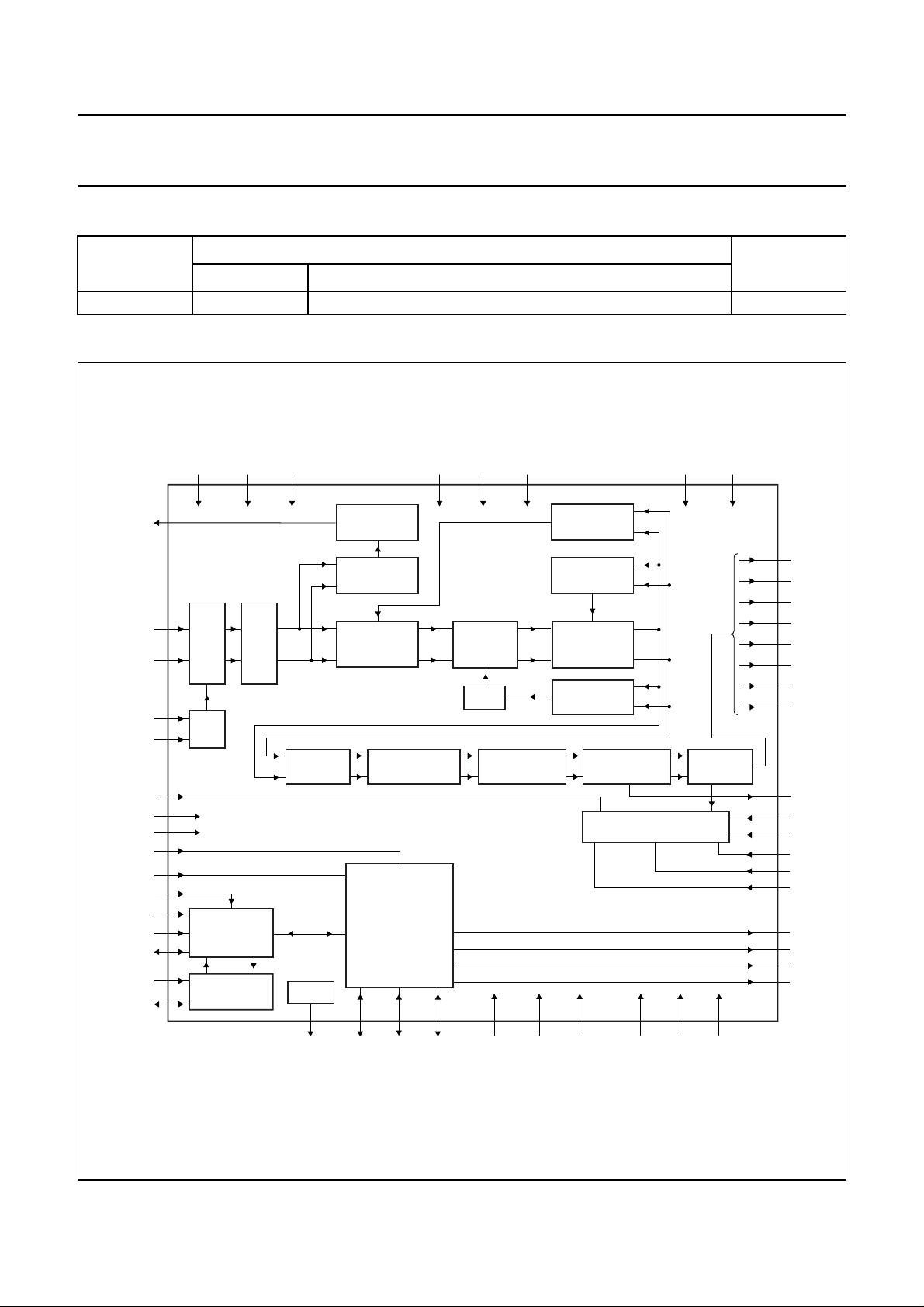
5 BLOCK DIAGRAM
handbook, full pagewidth
VAGC
VIN1
VIN2
XIN
XOUT
ENSERI
VREFN
VREFP
TMD
CLB#
SADDR0
IICDIV
SCL
SDA
SCL-0
SDA-0
VDDE57DVCC
24
30
15
ADC
12
DUAL 6-BIT
1
PLL
2
19
13
14
18
46
17
20
33
I2C-BUS
INTERFACE
32
29
I2C-BUS
28
TUNER SWITCH
VDDI
3, 8, 26,
38, 55
ADC OFFSET
CANCELLATION
VITERBI
DECODER
DISECQ
22K
PWM
ENCODER
AGC
DETECTION
COMPLEX
MULTIPLIER
DE-INTERLEAVER
PLLVCC
4
VDD3
FILTER
AVD
10
BANK
NCO
REED SOLOMON
DECODER
16
TDA10085HT
CONTROL
LOGIC
63 21 22 31 5 6
CTRL1 CTRL3 PLLGND DGDND
CTRL2
ADVD
42
CARRIER
SYNC
AGC
DETECTION
HALF-NYQUIST
FILTERS
CLOCK
SYNC
DE-SCRAMBLER
BOUNDARY SCAN
9, 25, 39,
56, 64
VSSI AVS ADVS VSSE
11
INTERFACE
43
VDDE
OUTPUT
23, 45,
58
27, 44,
57
62
DO7
61
DO6
60
DO5
59
DO4
54
DO3
53
DO2
52
DO1
51
DO0
37
FEL
34
TMS
35
TCK
36
TRST
40
TDI
41
TDO
47
PSYNC
48
UNCOR
49
DEN
50
OCLK
MGU427
Fig.1 Block diagram.
2001 Aug 31 4
Philips Semiconductors Product specification
Single chip DVB-S/DSS channel receiver TDA10085HT
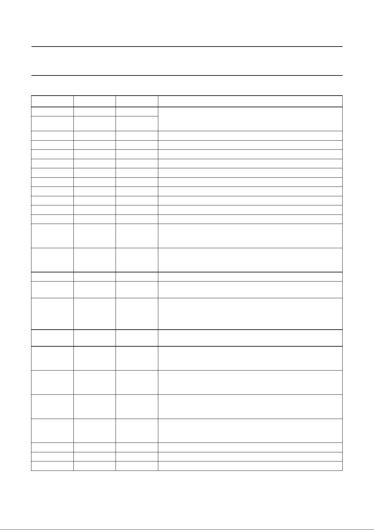
6 PINNING
SYMBOL PIN TYPE DESCRIPTION
XIN 1 I crystal oscillator input and output pins; in a typical application, a
XOUT 2 I
VDDI 3 supply digital core supply voltage (typically 1.8 V)
PLLVCC 4 supply analog supply voltage for the PLL (typically 3.3 V)
PLLGND 5 ground analog ground for the PLL
DGND 6 ground digital PLL core ground voltage; see note 2
DVCC 7 supply digital PLL core supply voltage (typically 1.8 V)
VDDI 8 supply digital ADC supply voltage (typically 1.8 V)
VSSI 9 ground digital ADC ground voltage; see note 2
VDD3 10 supply analog ADC supply voltage (typically 3.3 V)
AVS 11 ground analog ground voltage
VIN2 12 I analog signal input for channel Q; see note 1
VREFN 13 O negative analog voltage reference output (typically 1.25 V); a
VREFP 14 O positive analog voltage reference output (typically 2 V); a decoupling
VIN1 15 I analog signal input for channel I; see note 1
AVD 16 supply analog supply voltage (typically 3.3 V); a 0.1 µF decoupling capacitor
SADDR0 17 I SADDR0 input signal is the LSB of the I
TMD 18 I test input; must be connected to ground for normal operation; see
ENSERI 19 I enable serial interface input; when HIGH, the serial transport stream
IICDIV 20 I input to select the I
CTRL1 21 OD control line output 1; this pin function is directly programmable
CTRL2 22 OD control line output 2; this pin function is directly programmable
VSSE 23 ground digital ground voltage; see note 2
VDDE5 24 supply digital 5 V supply voltage; required for the 5 V tolerance of inputs
VSSI 25 ground digital core ground voltage; see note 2
fundamental oscillator crystal is connected between pins XIN and
XOUT; see note 1
decoupling capacitor (typically 0.1 µF) must be placed as close as
possible between VREFN and GND
capacitor (typically 0.1 µF) must be placed as closed as possible
between VREFP and GND
must be placed between AVD and AVS
2
C-bus address of the
TDA10085; other bits of the address are set internally to 000111,
therefore the complete I2C-bus address is (MSB to LSB):
0, 0, 0, 1, 1, 1 plus the SADDR0 bit; see note 1
note 1
is present on the boundary scan pins (TRST, TDO, TCK, TDI
and TMS); when LOW, the boundary scan pins are available; note 1
2
C-bus internal system clock frequency (depends
on the crystal frequency); internal I2C-bus clock is XIN when
IICDIV = 0 and XIN/4 if IICDIV = 1; see note 1
through the I
2
C-bus interface; default value is logic 1; open-drain
output requiring an external pull-up resistor to 3.3 V or to 5 V
through the I
2
C-bus interface; default value is logic 1; open-drain
output requiring an external pull-up resistor to 3.3 V or to 5 V
2001 Aug 31 5
 Loading...