Philips tda10085 DATASHEETS

INTEGRATED CIRCUITS
DATA SH EET
TDA10085
Single Chip DVB-S/DSS Channel
Receiver
Preliminary specification
File under Integrated Circuits, IC02
2000 March 16

Philips Semiconductors Preliminary specification
Single Chip DVB-S/DSS Channel Receiver TDA10085
FEATURES
• DSS and DVB-S compliant single chip demodulator & forward error correction.
• Dual 6-bit ADC on chip.
• New PLL which allows the use of a low-cost Xtal (typically 4 Mhz).
• DiSEqC 1.X from 1 to 8 bytes long sequences with modulated/unmodulated output.
• DSS dish control
• Digital Cancellation of A/D offset.
• Simultaneous Parallel and Serial Output interface.
• Variable rate BPSK/QPSK coherent demodulator.
• Modulation rate from 1 to 45MBaud.
• Automatic Gain Control output.
• Digital symbol timing recovery : Acquisition range up to ±
• Digital carrier recovery : Acquisition range up to 5Mhz
• Half Nyquist filters ( roll-off = 0.35 for DVB and 0.2 for DSS).
• Interpolating and anti-aliasing filters to handle variable symbol rate.
• Channel quality estimation.
• Spectral inversion ambiguity resolution.
• Viterbi decoder :
Supported rates : from 1/2 to 8/9.
Constraint length K = 7
with G1 = 171
Viterbi Output BER measurement.
Automatic code rate search within 1/2, 2/3 and 6/7 in DSS mode.
Automatic code rate search within 1/2, 2/3, 3/4, 5/6 and 7/8 in DVB-S mode.
• Convolutional deinterleaver and Reed Solomon decoder according to DVB and DSS specifications.
• Automatic Frame Synchronization.
• Selectable DVB-S descrambling.
2
C bus interface.
• I
• 64-pin TQFP package.
• CMOS technology (0.2 µ
G2 = 133
8
8
m 1.8V/3.3V).
960ppm
APPLICATIONS
• DVB-S receivers (ETS 300-421).
• DSS receivers.
DESCRIPTION
The TDA10085 is a single-chip channel receiver for satellite television reception which matches both DSS and
DVB-S standards. The device contains a dual 6-bit flash analog to digital converter, variable rate BPSK/Q PSK
coherent demodulator and Forward Error Correction functions. The ADCs directly interface with I and Q analog
baseband signals. After A to D conversion, the TDA10085 implements a bank of cascadable filters as well as
antialias and half-Nyquist filters. Analog AGC signal is generated by an amplitude estimation function. The
TDA10085 performs clock recovery at twice the Baud rate and achieves coherent demodulation without any
feedback to the local oscillator. Forward Error Correction is built around two error correcting codes : a ReedSolomon (outer code), and a Viterbi decoder (inner code). The Reed-Solomon decoder corrects up to 8 erroneous
bytes among the N (204) bytes of one data packet. Convolutional deinterleaver is located between the Viterbi
output and the R.S. decoder input. De-interleaver and R.S. decoder are automatically synchronized thanks to the
frame synchronisation algorithm which uses the sync pattern present in each packet. The TDA10085 is controlled
via an I2C bus interface. The circuit operates up to 100MHz and can process variable modulation rates, up to
45Mbaud.
The TDA10085 provides an interrupt line which can be programmed on either events or timing information.
Designed in 0.20 CMOS technology and housed in a 64-TQFP package, the TDA10085 operates over the
commercial temperature range.
2000 March 16 2

Philips Semiconductors Preliminary specification
Single Chip DVB-S/DSS Channel Receiver TDA10085
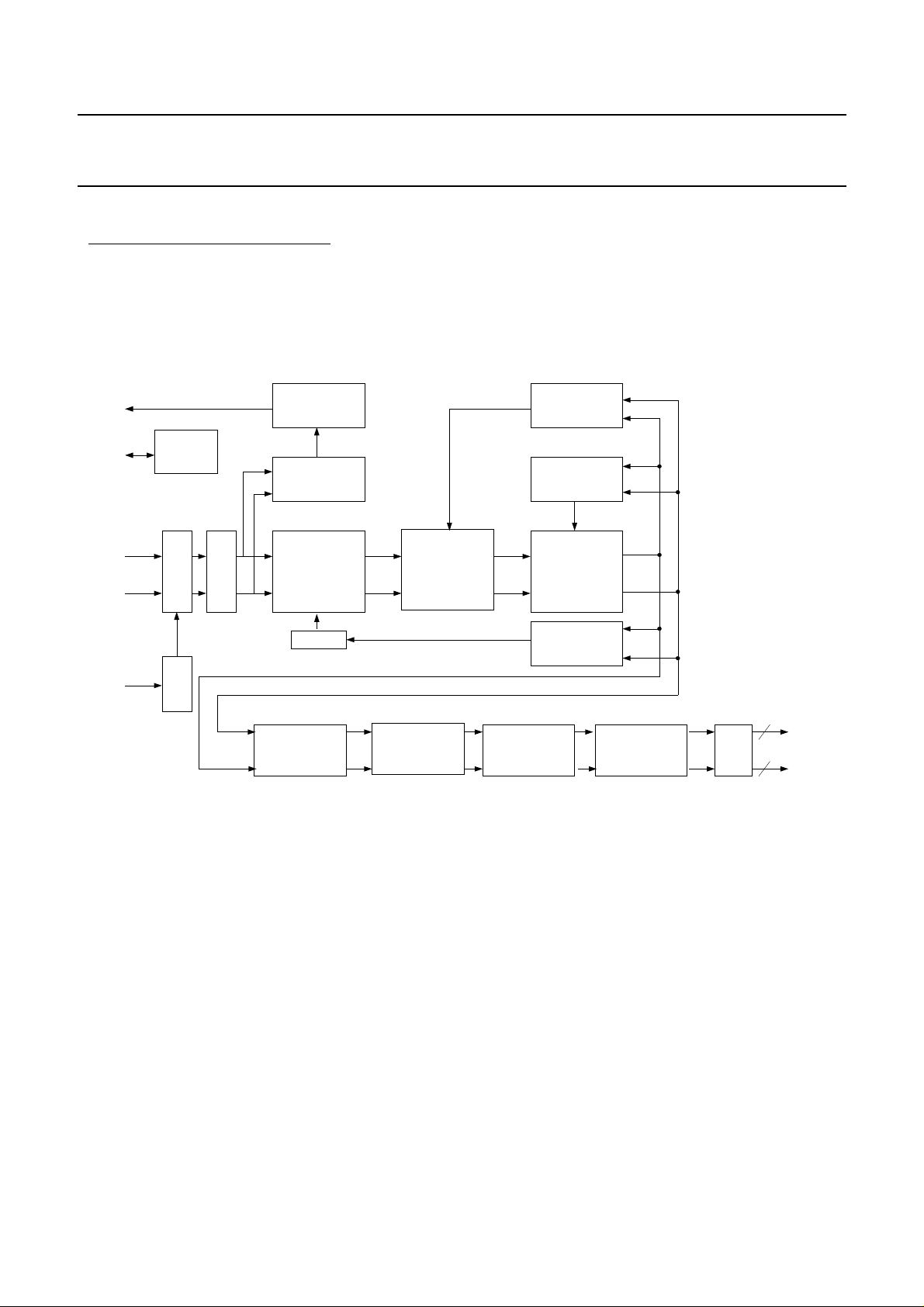
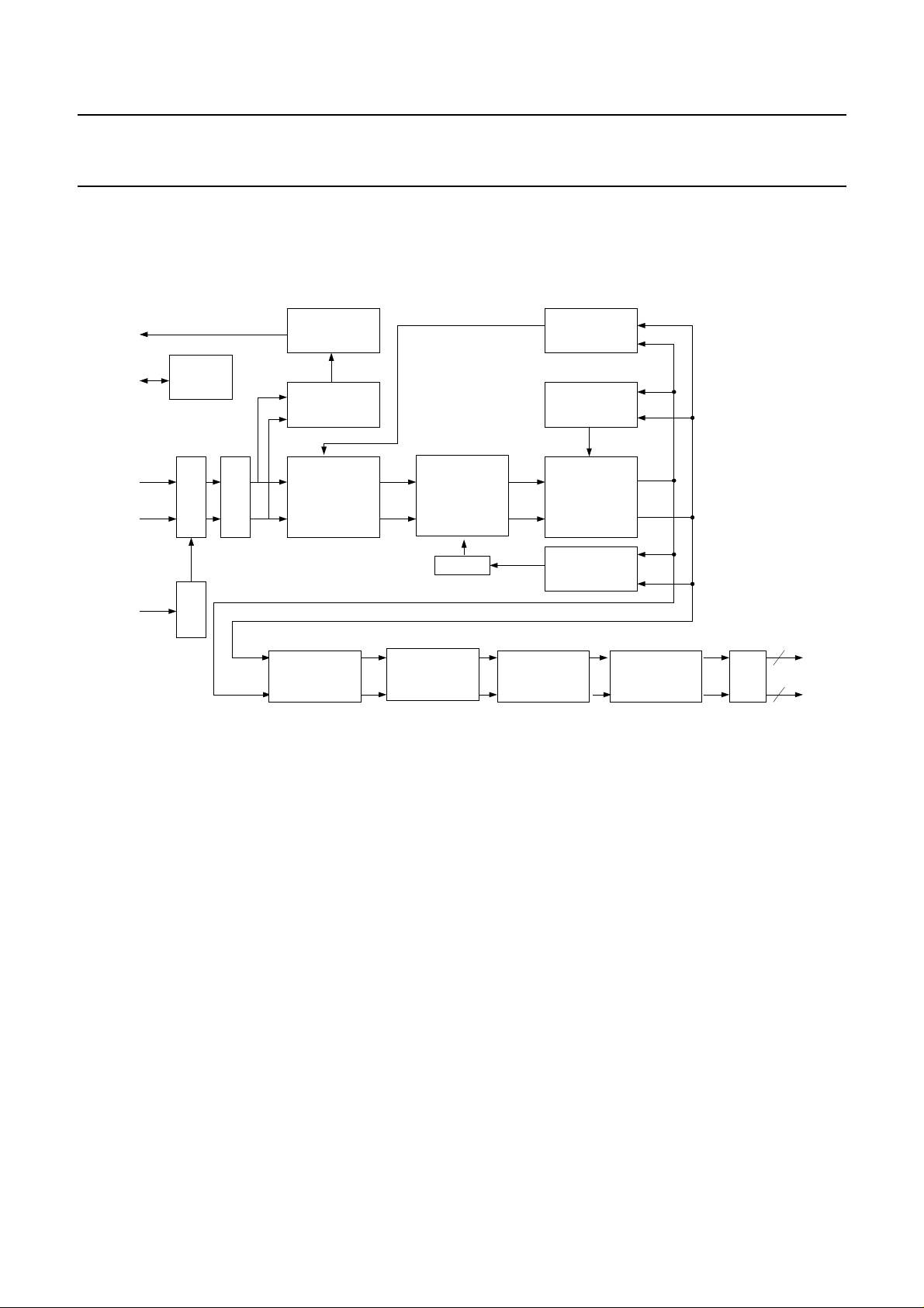
FIGURE 1. BLOCK DIAGRAM
1.1 WITH COMPLEX MULTIPLIER AFTER ANTI-ALIASING FILTERS (POSMUL=0) :
VAGC
VIN1
VIN2
XIN
I2C
INTERFACE
ADC
Dual 6-bit
PLL
PWM
ENCODER
AGC
DETECTION
FILTER BANK
ADC Offset
Cancellation
NCO
VITERBI
DECODER
COMPLEX
MULTIPLIER
DE-INTERLEAVER
REED SOLOMON
DECODER
CARRIER
SYNCHRO.
AGC
DETECTION
HALF-NYQUIST
FILTERS
CLOCK
SYNCHRO
DE-SCRAMBLER
Output
Interface
PARALLEL
TS
SERIAL
TS
2000 March 16 3

Philips Semiconductors Preliminary specification
Single Chip DVB-S/DSS Channel Receiver TDA10085
1.2 WITH COMPLEX MULTIPLIER BEFORE ANTI-ALIASING FILTERS (POSMUL=1) :
VAGC
VIN1
VIN2
XIN
I2C
INTERFACE
ADC
Dual 6-bit
PLL
PWM
ENCODER
AGC
DETECTION
COMPLEX
MULTIPLIER
ADC Offset
Cancellation
VITERBI
DECODER
DE-INTERLEAVER
FILTER
BANK
NCO
REED SOLOMON
DECODER
CARRIER
SYNCHRO.
AGC
DETECTION
HALF-NYQUIST
FILTERS
CLOCK
SYNCHRO
DE-SCRAMBLER
Output
Interface
PARALLEL
TS
SERIAL
TS
2000 March 16 4

Philips Semiconductors Preliminary specification
yp
Single Chip DVB-S/DSS Channel Receiver TDA10085
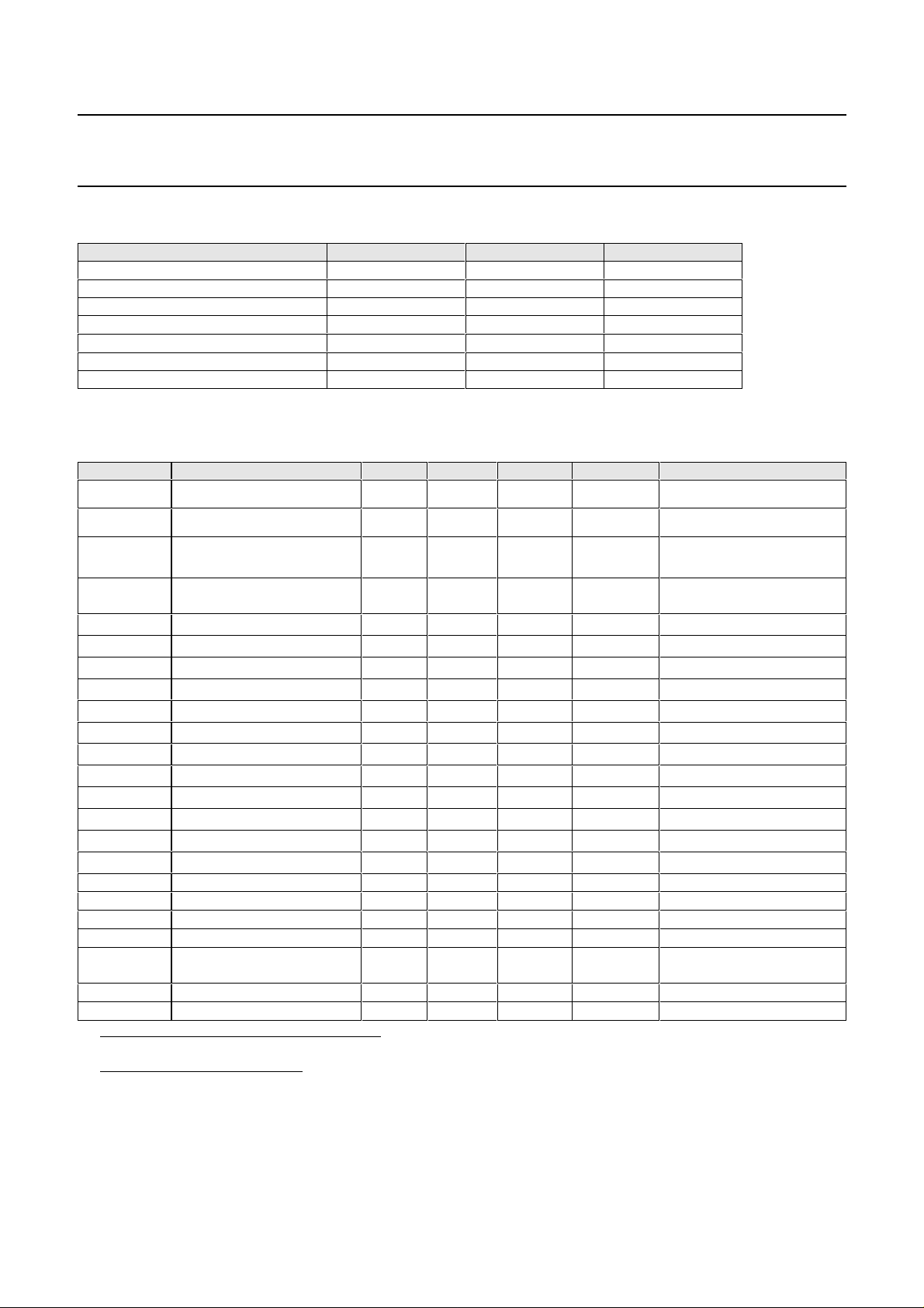
TABLE 1 : ABSOLUTE MAXIMUM RATINGS
Parameter Min Max Unit
Ambient operating temperature (Ta) 0 70 °C
DC supply voltage - 0.5 +4.1 V
DC Core supply voltage t.b.d t.b.d
DC input voltage - 0.5 VDD + 0.5 V
DC input current
Lead Temperature + t.b.d °C
Junction Temperature + t.b.d °C
Stresses above the absolute maximum ratings may cause permanent damage to the device. Exposure to absolute
maximum ratings conditions for extended periods may affect device reliability.
t.b.d
±
TABLE 2: RECOMMENDED OPERATING CONDITIONS
Symbol Parameter Min T
VDDE Digital supply voltage 3.0 3.3 3.6 V 3.3V ±10%
VDDI Digital Core Supply Voltage 1.62 1.8 1.98 V 1.8V ±10%
Max Unit Notes
mA
VDDE5 5V supply voltage
(for 5V Tolerance)
VDD3 3V ADC Digital
supply voltage
Ta Operating temperature 0 70 ° C
AVD Analog supply voltage 3.0 3.3 3.6 V
AVS Analog ground 0 V
VINDC DC Analog Input VREFN VREFP V
VINAC AC Analog Input 750 mVpp
ZIN Analog input impedance t.b.d t.b.d Ohms
CIN Analog input capacitance t.b.d t.b.d t.b.d pF
VREFP Top voltage reference t.b.d V
VREFN Bottom voltage reference t.b.d V
XIN Crystal frequency 4 Mhz MHz
SINAD (1) ADC signal to noise ratio t.b.d dB
THD(2) Total Harmonic Distorsion t.b.d dB
VIH(3) High-level input voltage t.b.d t.b.d V TTL input
VIL Low-level input voltage t.b.d t.b.d V TTL input
VOH(4) High-level output voltage t.b.d V @IOH = -2mA to -4mA
VOL(4) Low-level output voltage t.b.d V @IOL = + 2 mA to +4mA
IDD Supply current t.b.d mA/MBaud @XIN = 4Mhz/
CIN Input capacitance t.b.d pF 1MHz input to VSS
COUT Output capacitance t.b.d pF 1MHz input to VSS
(1) Signal-to-noise plus distortion ratio (SINAD) : ratio between the RMS magnitude of the fundamental input
frequency to the RMS magnitude of all other A/D output signals.
(2) Total harmonic distortion (THD
sample rate) to the fundamental.
(3) All inputs are 5V tolerant except CLB# pin.
(4) IOH, IOL = ±4mA only for pins : OCLK, SDA, SCL_0, SDA_0.
) : ratio of the RMS sum of all harmonics of the input signal (below one half of the
4.5 5 5.5 V pin 25
3.3
96 Mhz Sampling
2000 March 16 5
 Loading...