

Philips tda10045 DATASHEETS

INTEGRATED CIRCUITS
DATA SH EET
TDA10045
Single Chip DVB-T Channel
Receiver
Preliminary specification
File under Integrated Circuits, IC02
2000 March 15

Philips Semiconductors Preliminary specification
Single Chip DVB-T Channel Receiver TDA10045
FEATURES
• 2K and 8K COFDM demodulator (Fully DVB-T compliant : ETS 300-744).
• All modes supported including hierarchical modes.
• Fully automatic transmission parameters detection.
• DSP based synchronization (upgradability).
• No extra-host software required.
• On chip 10-bit ADC.
nd
or 1st IF variable analog input.
• 2
• Only fundamental Crystal oscillator needed.
• Frequency offset estimator to speed up the scan.
• RF Tuner input power measurement
• Parallel or serial transport stream interface.
• On chip FEC decoder.
• BER measurement (before and after Viterbi decoder)
• SNR estimation
• TPS bits I2C readable (including spare ones)
• Channel frequency response output.
• Controllable dedicated I2C tuner bus (5V tolerant).
• 2 low frequency spare DAC. (∆Σ
• Spare I/O.
• CMOS 0.2
m technology.
µ
)
APPLICATIONS
• DVB-T fully compatible.
• Digital data transmission using COFDM modulations.
DESCRIPTION
The TDA10045 is a single chip channel receiver for 2K and 8K COFDM modulated signals based on the ETSI
specification (ETSI 300 744). The device interfaces directly to an IF signal, which could be either first or second
IF and integrates a 10-bit AD converter, a NCO and a PLL, simplifying external logic r equirements and limiting
system costs.
The TDA10045 performs all the COFDM demodulation tasks from IF signal to the MPEG2 tr ansport stream. An
internal DSP core manages the synchronization and the control of the demodulation process, and implements
specialy developed software for robustness against co and adjacent channel interferers, to deal with SFN echoes
situations, and to help for a very fast scan of the bandwidth.
After base band conversion and FFT demodulation, the channel frequency response is estimated based on the
scattered pilots, filtered in both time and frequency domains. This estimation is used as a correction on the
signal, carrier by carrier. A common phase error and estimator is used to deal with the tuner phase noise.
The FEC decoder is automatically synchronized thanks to the frame synchronization algorithm that uses the TPS
information included in the modulation.
This device is controlled via an I2C bus (called master). The chip provides 2 switchable I2C bus derived from the
master. A tuner I2C bus to be disconnected from the I2C master when not necessary and an Eeprom I2C bus.
The DSP software code can be fed to the chip via the master I2C bus or via the dedicated Eeprom I2C bus.
Designed in 0.2 µm CMOS technology and housed in a 100-pin MQFP package, the TDA10045 operates over
the commercial temperature range.
2000 March 15 2
Philips Semiconductors Preliminary specification
Single Chip DVB-T Channel Receiver TDA10045
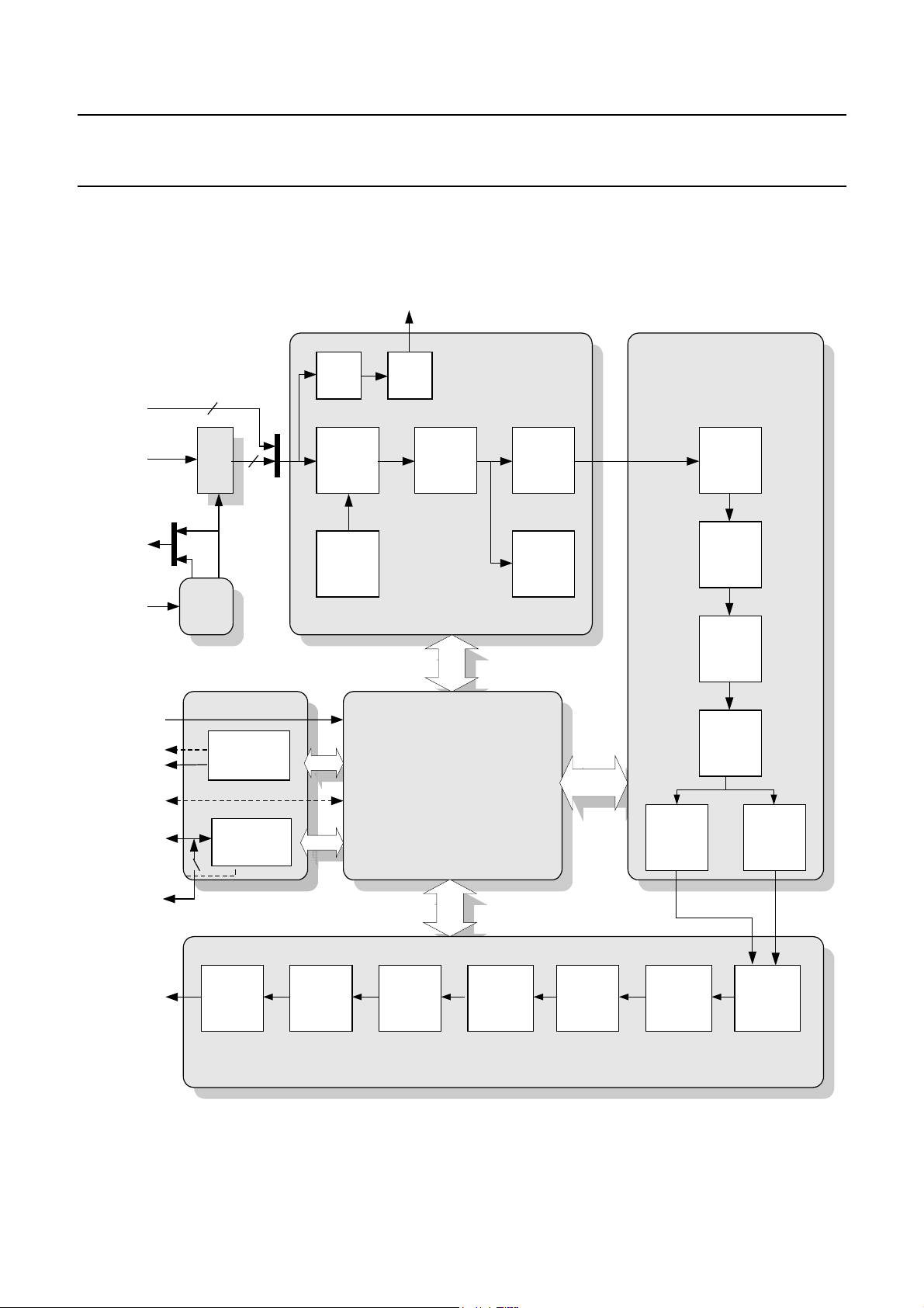
),*85(,17(51$/%/2&.',$*5$0
VAGC
Digital IF
FI(9:0)
Analog IF
(VIM,VIP)
SACLK
XIN
SP-IN(1:0)
CTRL_VCXO
DS_SPARE(1:0)
SCL_EEP
SDA_EEP
SCL
SDA
10
Fsamp
2Fsamp
PLL
A
D
C
spare inputs
3 spare
optional
I2C
Interface
AGC
∆Σ
AND OFDM
DEMODULATION
DIGITAL FRONT-END
10
Base
Band
Conversion
NCO
Carrier
Recovery
FFT
Coarse
Time
Estimator
OAK+ DSP CORE
∆Σ
3 * 10
SYNCHRONISATION
CHANNEL ESTIMATION
AND CORRECTION
OFDM
Spectrum
CPE
Calculation
Partial
Channel
Estimation
Time
Interpolation
Frequency
Interpolation
Frequency, Timing, Frame Recovery
FFT Window positioning
TPS decoding
Confidence
Calculation
Channel
Correction
SCL_TUN
SDA_TUN
DO
OCLK
DEN
PSYNC
UNCOR
MPEG2
Output
Interface
Descrambler
RS
decoder
CHANNEL DECODER
2000 March 15 3
Outer
Forney
Deinterleaver
Confidence
Frequency
response
Viterbi
Decoder
VBER CBERCPT_UNCOR
Bit
Deinterleaver
(I,Q)
Constellation
Inner
Frequency
Deinterleaver
& Demapper

Philips Semiconductors Preliminary specification
Single Chip DVB-T Channel Receiver TDA10045
,13872873876,*1$/'(6&5,37,21
SYMBOL PIN NUMBER TYPE DESCRIPTION
CLOCK AND RESET SIGNALS
CLR# 14 I Asynchronous reset signal, active low
XIN
XOUT 79 O Crystal oscillator output pin.
SACLK
CTRL_VCXO
80
33
(3.3V)
3O
(3.3V)
DEMODULATOR SIGNALS
FI[9:0] 34-35-36-37-38-
41-42-43-44-45
30
FFT_WIN
VAGC 4 O
FEL
IT
49 0D
48
IO TRI Input data fr om an external ADC, FI must be tied to ground when not
IO TRI
(3.3V)
(5V)
(5V)
Crystal oscillator input pin. Typically a fundamental XTAL oscillator is
I
connected between XIN and XOUT.
Sampling frequency output. This output clock can be fed to an external
O
(10-bit) ADC as sampling clock. Depending on “Sel_Saclk” (Reg
CONFADC), SACLK could also provide twice the sampling clock.
If not in NCO mode, control of an external sampling VCXO (after lowpass filtering)
used, positive notation (from 0 to 1023) or two's complement notation
(from -512 to 511). In internal ADC mode, these outputs can be used
to monitor extra demodulator output signal (constellation, frequency
response).
Output or input signal indicating the start of the active data; equals 1
during complex sample 0 of the active FFT block. Can be used to
synchronize 2 chips.
output value from the Delta-Sigma Modulator, used to control a logscaled amplifier (after analog filtering )
front end lock. FEL is an output drain output and therefore requires an
external pull up resistor.
Interrupt line. This output interrupt line can be configured by the I2C
OD
interface. See registers Itsel and Itstat. IT is an open drain output and
therefore requires an external pull up resistor.
FEC OUTPUTS
DO[7:0] 67-68-69-72-73-
74-75-76
OCLK 66 O
DEN 65 O
PSYNC 64 O
UNCOR 63 O
2000 March 15 4
O
(3.3V)
(3.3V)
(3.3V)
(3.3V)
(3.3V)
output data carrying the current sample of the current MPEG2 packet
(188 bytes), delivered on the rising edge of OCLK by default. When
the serial mode is selected, the output data is delivered by DO[0].
Output CLock. OCLK is the output clock for the parallel DO[7:0]
outputs. (may be inverted, see POCLK and DISABLE_TS I2C
registers)
output data validation signal active high during the valid and regular
data bytes (may be inverted, see PDEN and DISABLE_TS I2C
registers).
Pulse Synchro. This output signal goes high on a rising edge of OCLK
when a synchro byte is provided, then goes low until the next synchro
byte (may be inverted, see PPSYNC and DISABLE_TS I2C registers).
RS error flag, active high on one RS packet if the RS decoder fails in
correcting the errors (may be inverted, see PUNCOR and
DISABLE_TS I2C registers).

Philips Semiconductors Preliminary specification
Single Chip DVB-T Channel Receiver TDA10045
ON-CHIP ADC SIGNALS
92
VIM
91
VIP
VREFP
VREFM
VD1
VS1 99 I Ground return for the digital switching circuitry.
VD2
VS2 97 I Ground return for the analog clock drivers.
VD3
VS3 96-89 I Ground return for analog circuits.
94
93
100
98
95-90
Negative input to the A/D converter. This pin is DC biased to half
supply through an internal resistor divider (2x20K resistors). In order
I
to remain in the range of the ADC, the voltage difference between pins
VIP and VIM should be between -0.5 and 0.5 volts (See SW I2C
register).
Positive input to the A/D converter. This pin is DC biased to half supply
through an internal resistor divider (2x20K resistors). In order to
I
remain in the range of the ADC, the voltage difference between pins
VIP and VIM should be between –0.5 and 0.5 volts.
Positive voltage reference for the A/D converter. See SW I2C register
O
for the output level.
Negative voltage reference for the A/D converter. See SW I2C register
O
for the output level.
Power supply input for the digital switching circuitry sensitive to the
I
supply noise. The DC voltage should be 1,8V.
Power supply input for the analog clock drivers. The DC voltage should
I
be 3.3V.
Power supply input for the analog circuits. The DC voltage should be
I
3.3V.
I2C INTERFACES
SCL 11 I I2C master serial clock. Up to 700 kbit/s.
SDA 12 I/O I2C master serial data inout, open drain I/O pad.
16-17
SADDR[1:0]
9
SCL_TUN
10
SDA_TUN
SCL_EEP 5 O Extra I2C clock to download DSP code from an external EEPROM.
SDA_EEP 8 I/O Extra I2C data bus to download DSP code from an external
15
EEPADDR
SADDR[1:0] are the 2 LSBs of the I2C address of the TDA10045. The
I
MSBs are internally set to 00010. Therefore the complete I2C address
of the TDA10045 is (MSB to LSB): 0,0,0,1,0,SADDR[1], SADDR[0]
Tuner I2C serial clock signal.This signal derived from the master SCL
OD
can be set to high impedance when no tuner acces needed. (See
BP_I2C_TUN register) (open drain)
Tuner I2C serial data signal.This signal derived from the master SDA
I/O
can be set to high impedance when no tuner acces needed. (See
BP_I2C_TUN register) (open drain)
(Optional mode). Can be connected to the master I2C Bus. (open
drain)
EEPROM. (Optional mode). Can be connected to the master I2C Bus.
(open drain)
EEPRAD is the LSB of the I2C address of the EEPROM. The MSBs
I
are internally set to 101000. Therefore the complete I2C address of
the EEPROM is (MSB to LSB): 1,0,1,0,0,0, EEPADDR
2000 March 15 5
 Loading...