

Philips sstl16877 DATASHEETS
INTEGRATED CIRCUITS
SSTL16877
14-bit SSTL_2 registered driver with
differential clock inputs
Product specification
Supersedes data of 2000 Apr 20
2000 Aug 15
Philips Semiconductors Product specification
14-bit SSTL_2 registered driver with
differential clock inputs
FEA TURES
•Stub-series terminated logic for 2.5 V VDDQ (SSTL_2)
•Optimized for DDR (Double Data Rate) SDRAM applications
•Supports SSTL_2 signal inputs and outputs
•Flow-through architecture optimizes PCB layout
•Meets SSTL_2 class I and class II specifications
•Latch-up protection exceeds 500mA per JEDEC Std 17
•ESD protection exceeds 2500 V per MIL STD 833 Method 3015
and 200 V per Machine Model
•Full DDR1 PC333 solution @ 2.5 V when used with PCKV857
•Mixed 2.5 V (PC266) / 3.3 V (PC333) solution when used with
PCK857
•Same form, fit, and function as SSTV16857
DESCRIPTION
The SSTL16877 is a 14-bit SSTL_2 registered driver with differential
clock inputs, designed to operate between 2.3 V and 2.7 V . V
must not exceed VCC. Inputs are SSTL_2 type with V
0.5*V
. The outputs support class I which can be used for
DDQ
standard stub-series applications or capacitive loads. Master reset
(RESET
) asynchronously resets all registers to zero.
The SSTL16877 is intended to be incorporated into standard DIMM
(Dual In-Line Memory Module) designs defined by JEDEC, such as
DDR (Double Data Rate) SDRAM or SDRAM II Memory Modules.
Different from traditional SDRAM, DDR SDRAM transfers data on
both clock edges (rising and falling), thus doubling the peak bus
bandwidth. A DDR DRAM rated at 166 MHz will have a burst rate of
333 MHz. The modules require between 23 and 27 registered
control and address lines, so two 14-bit wide devices will be used on
each module. The SSTL16877 is intended to be used for SSTL_2
input and output signals.
The device data inputs consist of differential receivers. One
differential input is tied to the input pin while the other is tied to a
reference input pad, which is shared by all inputs.
The clock input is fully differential to be compatible with DRAM
devices that are installed on the DIMM. However, since the control
inputs to the SDRAM change at only half the data rate, the device
must only change state on the positive transition of the CLK signal.
In order to be able to provide defined outputs from the device even
before a stable clock has been supplied, the device must support an
asynchronous input pin (reset), which when held to the LOW state
will assume that all registers are reset to the LOW state and all
outputs drive a LOW signal as well.
normally at
REF
DDQ
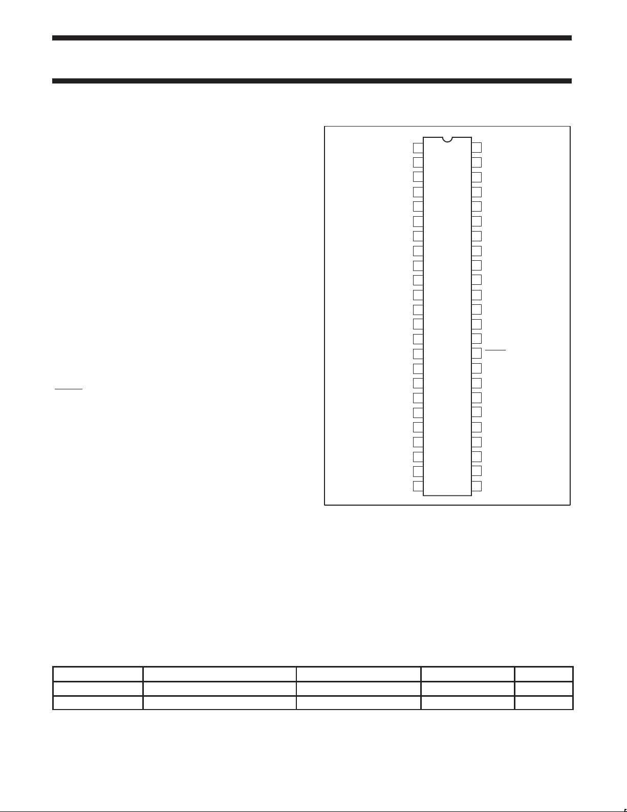
PIN CONFIGURATION
1
Q1
2
Q2
3
GND
VDDQ
4
5
Q3
6
Q4
Q5
7
8
GND
9
VDDQ
Q6
10
11
Q7
12
VDDQ
13
GND
14
Q8
Q9
15
16
VDDQ
17
GND
Q10
18
19
Q11
20
Q12
21
VDDQ
GND
22
Q13
23
24
Q14
SSTL16877
48
D1
47
D2
46
GND
45
VCC
44
D3
43
D4
42
D5
41
D6
40
D7
39
CLK–
38
CLK+
37
VCC
36
GND
35
VREF
34
RESET
33
D8
32
D9
31
D10
30
D11
29
D12
28
VCC
27
GND
26
D13
25
D14
SW00311
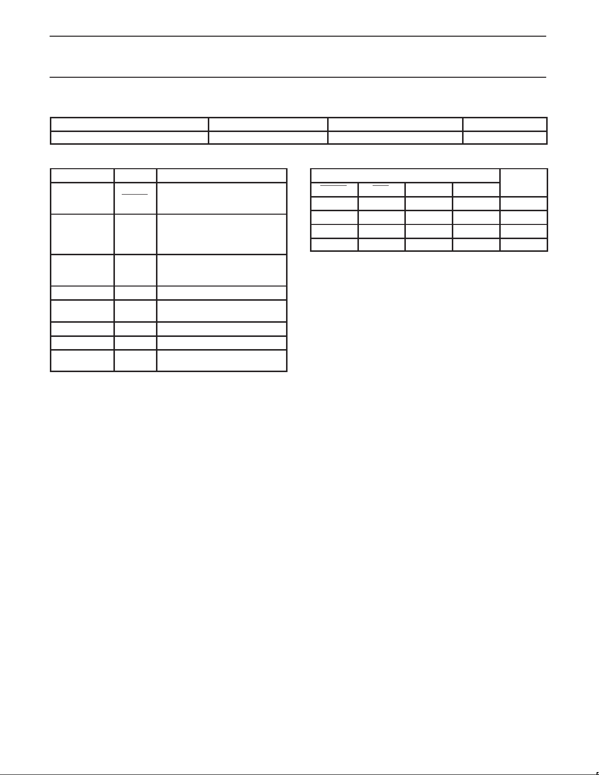
QUICK REFERENCE DA TA
GND = 0 V; T
SYMBOL
t
PHL/tPLH
NOTES:
1. C
is used to determine the dynamic power dissipation (PD in µW) PD = CPD V
PD
= input frequency in MHz; CL = output load capacity in pF; fo = output frequency in MHz; VCC = supply voltage in V;
f
i
ȍ (C
L
2000 Aug 15 853-2198 23523
= 25°C; tr =tf v2.5 ns
amb
C
I
2
V
fo) = sum of the outputs.
CC
PARAMETER CONDITIONS TYPICAL UNIT
Propagation delay; CLK to Qn CL = 30 pF; V
= 2.5 V 2.4 ns
DDQ
Input capacitance VCC = 2.5 V 2.9 pF
2
x fi )ȍ (CL V
CC
2
fo) where:
CC
2
Philips Semiconductors Product specification
14-bit SSTL_2 registered driver with
differential clock inputs
ORDERING INFORMATION
PACKAGES TEMPERATURE RANGE ORDER CODE DWG NUMBER
48-Pin Plastic TSSOP Type I 0°C to +70°C SSTL16877 DGG SOT362-1
PIN DESCRIPTION
PIN NUMBER SYMBOL NAME AND FUNCTION
LVCMOS asynchronous master
34 RESET
48, 47, 44, 43,
42, 41, 40, 33,
32, 31, 30, 29,
26, 25
1, 2, 5, 6, 7, 10,
11, 14, 15, 18,
19, 20, 23, 24
35 VREF SSTL_2 input reference level
3, 8, 13, 17, 22,
27, 36, 46
28, 37, 45 V
4, 9, 12, 16, 21 V
38
39
D1 – D14 SSTL_2 data inputs
Q1 – Q14 SSTL_2 data outputs
GND Ground (0 V)
DDQ
CLK+
CLK–
reset
(Active LOW)
Positive supply voltage
CC
Output supply voltage
Differential clock inputs
FUNCTION TABLE
INPUTS
RESET CLK CLK D
L X X X L
H ↓ ↑ H H
H ↓ ↑ L L
H L or H L or H X Q
H = High voltage level
L = High voltage level
↓ = High-to-Low transition
↑ = Low-to-High transition
X = Don’t care
SSTL16877
OUTPUT
Q
0
2000 Aug 15
3
 Loading...