

Philips NE567N, NE567D, SE567D, SE567N Datasheet
Philips Semiconductors Linear Products Product specification
NE/SE567Tone decoder/phase-locked loop
403
April 15, 1992 853-0124 06456
DESCRIPTION
The NE/SE567 tone and frequency decoder is a highly stable
phase-locked loop with synchronous AM lock detection and power
output circuitry. Its primary function is to drive a load whenever a
sustained frequency within its detection band is present at the
self-biased input. The bandwidth center frequency and output delay
are independently determined by means of four external
components.
FEATURES
•Wide frequency range (.01Hz to 500kHz)
•High stability of center frequency
•Independently controllable bandwidth (up to 14%)
•High out-band signal and noise rejection
•Logic-compatible output with 100mA current sinking capability
•Inherent immunity to false signals
•Frequency adjustment over a 20-to-1 range with an external
resistor
•Military processing available
APPLICATIONS
•Touch-Tone decoding
•Carrier current remote controls
•Ultrasonic controls (remote TV, etc.)
•Communications paging
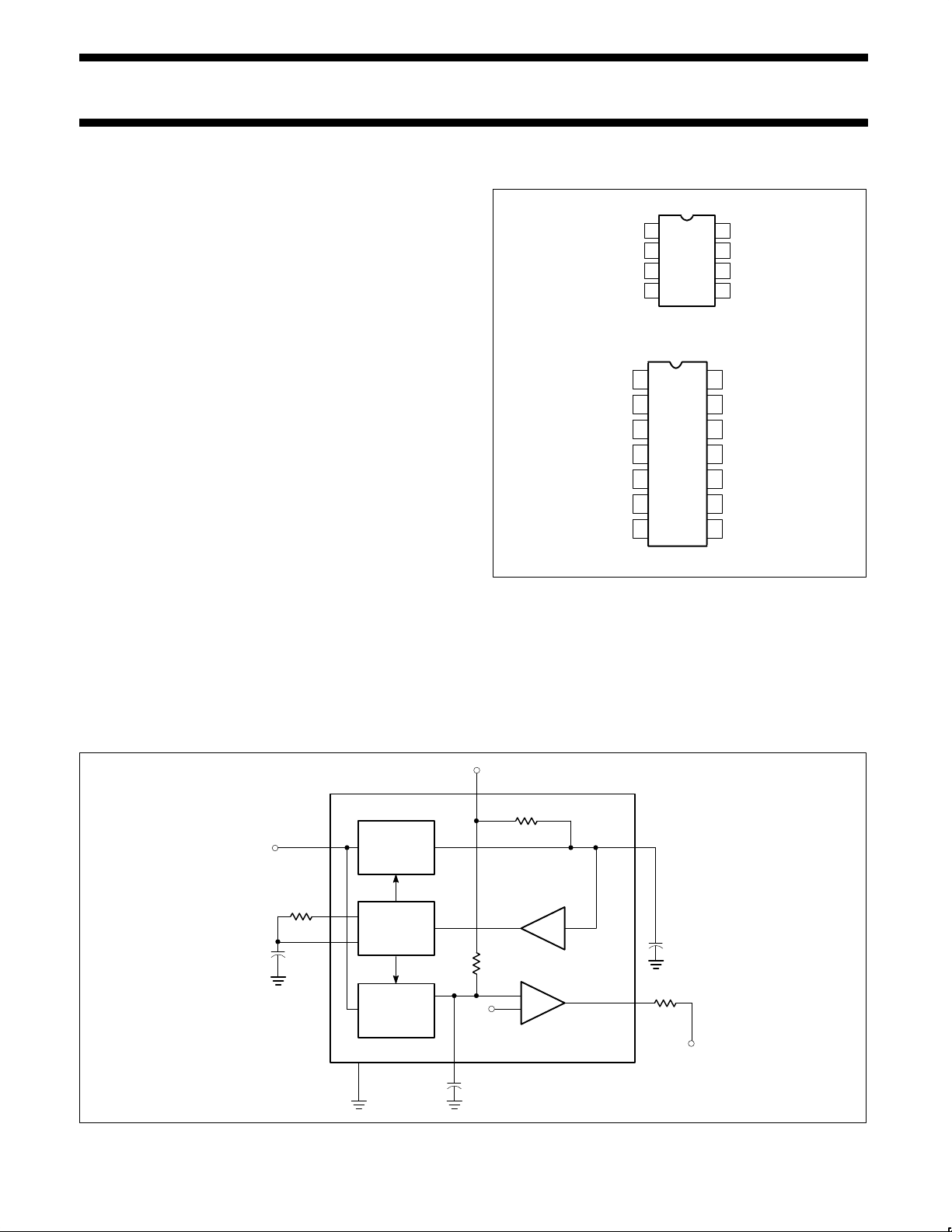
PIN CONFIGURATIONS
FE, D, N Packages
F Package
1
2
3
4 5
6
7
8
1
2
3
4
5
6
7 8
14
13
12
11
10
9
OUTPUT FILTER
CAPACITOR C3
LOW-PASS FILTER
CAPACITOR C2
INPUT
SUPPLY VOLTAGE V+
OUTPUT
GROUND
TIMING
ELEMENTS R1
AND C1
TIMING ELEMENT R1
OUTPUT
C3
NC
C2
INPUT
NC
V
CC
GND
NC
NC
R1C1
R1
NC
NC
TOP VIEW
TOP VIEW
•Frequency monitoring and control
•Wireless intercom
•Precision oscillator
BLOCK DIAGRAM
Touch-Tone is a registered trademark of AT&T.
INPUT
V1
PHASE
DETECTOR
CURRENT
CONTROLLED
OSCILLATOR
QUADRATURE
PHASE
DETECTOR
AMP
AMP
LOOP
LOW
PASS
FILTER
3
5
6
7 1
8
2
4
3.9k
+
–
+V
FILTER
C
1
R
1
R
2
R
3
R
L
V
REF
C
2
C3 OUTPUT
Philips Semiconductors Linear Products Product specification
NE/SE567Tone decoder/phase-locked loop
April 15, 1992
404
EQUIVALENT SCHEMATIC
–V
4
R5
Q1
5
R1
6
C1
Q2
7
Q8
Q3
R6
Q10 D
R7
Q12
Q13
–V
Q6
Q7
A
Q9
R4
Q5
R9
Q14
Q16
Q17
Q19 B
R19
R12
Q22
–V
R15
Q25
Q24
Q26
Q27 Q28
Q29 B
R18
R10
R11
–V
R20
R13
E F
Q23
Q30
B
R14
R16
R17
R23
R24
R21
R2
10k
Q20
R26
Q21
R22
A
Q34
R29
3
C
Vi
2
C2
–V
Q35
R30
R26
R27
Q33
Q36Q37
R36
Q50
R37
Q62
Vref
Q59
R40
F
E
R32
R48
21k
R48
21k
Q40
C
Q30
Q38
R36
R34
Q61
R36
Q16
Q18
Q31 B
R28
Q40
R33
R39
5k
R41
Q63
Q55
R48
Q60
C
R43
Q47
Q46 Q45 Q44
Q43
Q42
Q41
B
R44
Q62
Q61
R45
B
RL
–V
R49
C3
1
R3
4.7k
R42
Q54
Q57Q56
Q58
Q32
c
Philips Semiconductors Linear Products Product specification
NE/SE567Tone decoder/phase-locked loop
April 15, 1992
405
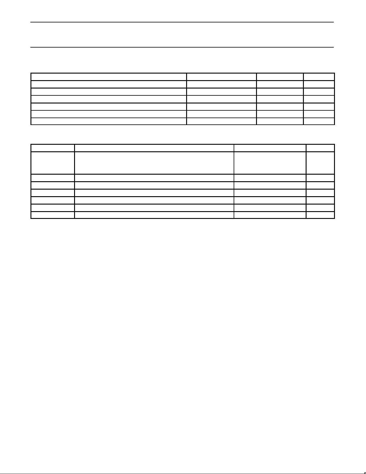
ORDERING INFORMATION
DESCRIPTION TEMPERATURE RANGE ORDER CODE DWG #
8-Pin Plastic SO 0 to +70°C NE567D 0174C
14-Pin Cerdip 0 to +70°C NE567F 0581B
8-Pin Plastic DIP 0 to +70°C NE567N 0404B
8-Pin Plastic SO -55°C to +125°C SE567D 0174C
8-Pin Cerdip -55°C to +125°C SE567FE 0581B
8-Pin Plastic DIP -55°C to +125°C SE567N 0404B
ABSOLUTE MAXIMUM RATINGS
SYMBOL PARAMETER RATING UNIT
T
A
Operating temperature
NE567 0 to +70 °C
SE567 -55 to +125 °C
V
CC
Operating voltage 10 V
V+ Positive voltage at input 0.5 +V
S
V
V- Negative voltage at input -10 V
DC
V
OUT
Output voltage (collector of output transistor) 15 V
DC
T
STG
Storage temperature range -65 to +150 °C
P
D
Power dissipation 300 mW
Philips Semiconductors Linear Products Product specification
NE/SE567Tone decoder/phase-locked loop
April 15, 1992
406
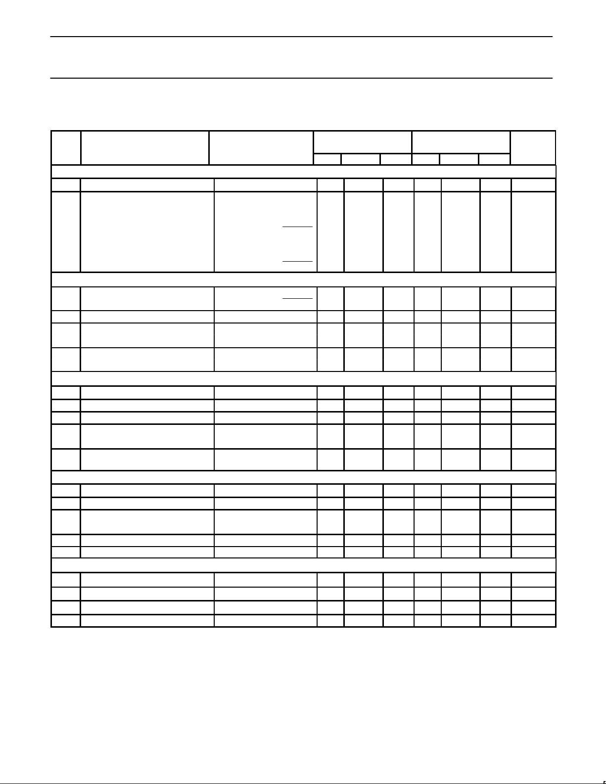
DC ELECTRICAL CHARACTERISTICS
V +=5.0V; TA=25°C, unless otherwise specified.
SYM-
BOL
PARAMETER TEST CONDITIONS SE567 NE567 UNIT
Min Typ Max Min Typ Max
Center frequency
1
f
O
Highest center frequency 500 500 kHz
f
O
Center frequency stability
2
-55 to +125°C 35 ±140 35 ±140 ppm/°C
0 to +70°C 35 ±60 35 ±60 ppm/°C
f
O
Center frequency distribution
fO 100kHz
1
1.1R
1C1
-10 0 +10 -10 0 +10 %
f
O
Center frequency shift with supply
voltage
fO 100kHz
1
1.1R
1C1
0.5 1 0.7 2 %/V
Detection bandwidth
BW Largest detection bandwidth
fO 100kHz
1
1.1R
1C1
12 14 16 10 14 18 % of f
O
BW Largest detection bandwidth skew 2 4 3 6 % of f
O
BW Largest detection bandwidth— VI=300mV
RMS
±0.1 ±0.1 %/°C
variation with temperature
BW Largest detection bandwidth— VI=300mV
RMS
±2 ±2 %/V
variation with supply voltage
Input
R
IN
Input resistance 15 20 25 15 20 25 kΩ
V
I
Smallest detectable input voltage
4
IL=100mA, fI=f
O
20 25 20 25 mV
RMS
Largest no-output input voltage
4
IL=100mA, fI=f
O
10 15 10 15 mV
RMS
Greatest simultaneous out-band +6 +6 dB
signal-to-in-band signal ratio
Minimum input signal to wide-band
noise ratio
Bn=140kHz -6 -6 dB
Output
Fastest on-off cycling rate fO/20 fO/20
“1” output leakage current V8=15V 0.01 25 0.01 25 µA
“0” output voltage IL=30mA 0.2 0.4 0.2 0.4 V
IL=100mA 0.6 1.0 0.6 1.0 V
t
F
Output fall time
3
RL=50Ω 30 30 ns
t
R
Output rise time
3
RL=50Ω 150 150 ns
General
V
CC
Operating voltage range 4.75 9.0 4.75 9.0 V
Supply current quiescent 6 8 7 10 mA
Supply current—activated RL=20kΩ 11 13 12 15 mA
t
PD
Quiescent power dissipation 30 35 mW
NOTES:
1. Frequency determining resistor R
1
should be between 2 and 20kΩ
2. Applicable over 4.75V to 5.75V. See graphs for more detailed information.
3. Pin 8 to Pin 1 feedback R
L
network selected to eliminate pulsing during turn-on and turn-off.
4. With R
2
=130kΩ from Pin 1 to V+. See Figure 1.
 Loading...