

Philips ne5562, se5562 DATASHEETS

Philips Semiconductors Product specification
NE/SE5562Switched-mode power supply control circuit
1
1994 Aug 31 853-0811 13721
DESCRIPTION
The NE/SE5562 is a single-output control circuit for switched-mode
power supplies. This single monolithic IC contains all control and
protection features needed for full-featured switched-mode power
supplies.
The 100mA source/sink output is designed to drive power FETs
directly. The associated output logic is designed to prevent double
pulsing or cross-conduction current spiking on the output.
All of the control and protect features work cycle-by-cycle up to the
maximum operating frequency of 600kHz.
For ease of interface, all digital inputs are TTL or CMOS compatible.
The NE5562 is supplied in 20-pin glass/ceramic (Cerdip), plastic
DIP, and plastic SO packages. The NE grade part is characterized
and guaranteed over the commercial ambient temperature range of
0°C to +70°C and junction temperature range of 0°C to +85°C. The
SE5562 is supplied in the glass/ceramic (Cerdip) package. The SE
grade part is characterized and guaranteed over the ambient
temperature range of -55 to +125°C and junction temperature range
of -55 to +135°C.
FEATURES
•Stabilized power supply
•Temperature-compensated reference source
•Sawtooth generator
•Pulse width modulator
•Remote on/off switching
•Current limiting (2 levels)
PIN CONFIGURATION
1
2
3
4
5
6
7
8
9
10
11
12
13
14
20
19
18
17
16
15
D, F, N Packages
TOP VIEW
FEED FORWARD
EXTERNAL MOD IN
DUTY CYCLE CONTROL
REMOTE ON/OFF
FEEDBACK VOLTAGE
ERROR AMP OUT
C
T
R
T
V
I
V
Z
GROUND
OUTPUT
DEMAG OVERVOLT IN
C DELAY
AUX COMP INPUT
CURRENT SENSE
OUT INVERT CONTROL
AUX COMP HYSTERESIS
V
S
EXTERNAL SYNC IN
SL00388
Figure 1. Pin Configuration
•Auxiliary comparator, with adjustable hysteresis
•Loop fault protection
•Demagnetization/overvoltage protection
•Duty cycle adjust and clamp
•Feed-forward control
•External synchronization
•Total shutdown after adjustable number of overcurrent faults
•Soft-start
ORDERING INFORMATION
DESCRIPTION TEMPERATURE RANGE ORDER CODE DWG #
20-Pin Plastic Small Outline (SO) Package 0 to +70°C NE5562D 1021B
20-Pin Plastic Dual In-Line Package (DIP) 0 to +70°C NE5562N SOT146-1
20-Pin Ceramic Dual In-Line Package (CERDIP) -55°C to +125°C SE5562F SOT146-1
Philips Semiconductors Product specification
NE/SE5562Switched-mode power supply control circuit
1994 Aug 31
2
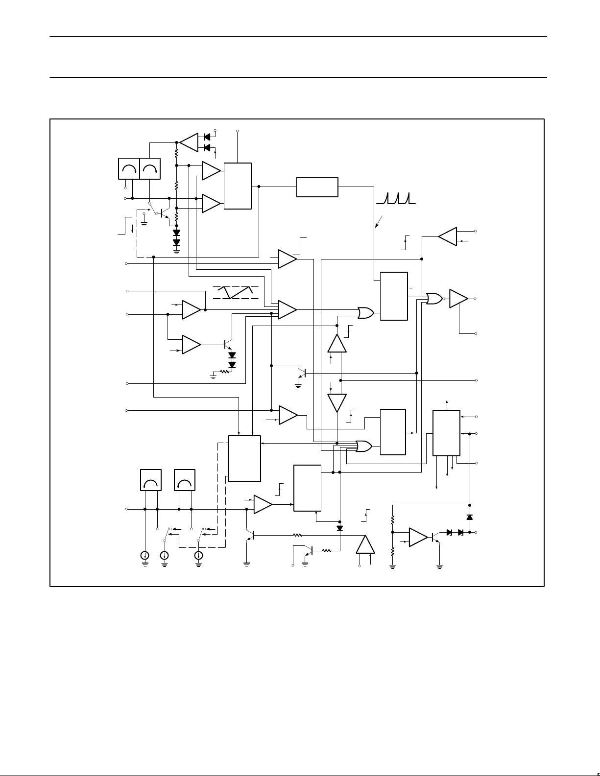
BLOCK DIAGRAM
FEEDFORWARD
1
11
EXTERNAL
SYNC IN
+
+
–
+
S
R
Q
OSC
LATCH
OSCILLATOR
3
2
OFF
ON
CLOCK
TIME
DELAY
OFF
ON
1.5V
REMOTE
ON/OFF
6
ERROR
AMP
OUT
10
FEEDBACK
VOLTAGE
8
EXTERNAL
MOD
IN
4
DUTY CYCLE
CONTROL
5
CLOCK
LOOP FAULT
COMP
0.955V
3.80V
PWM
COMP
ON/OFF
COMP
2k
OC1
0C2
0.955V
SLOW
START
COMP
OC2
NORM
–
+
0.528V
OVERCURRENT 1
COMP
OVERCURRENT 2
COMP
OC CHARGE PUMPS
NORM
LV STOP
START/
STOP
LATCH
R
S
Q
0.645V
OUTPUT
LATCH
OC1
NORM
LOW BULK
BULK
SENSE
COMP
1:1
1:1
16
POWER
SUPPLY
CKTS
3.80V
SHUT
DOWN
LATCH
3.80V
OC ACCUM
COMP
TRIP
NORM
S
R
Q
–
+
+V
+V
OC1 OC2
AUXILIARY
COMP
HYSTERESIS
AUXILIARY
COMP
INPUT
12
ERROR
AMP
DEMAG/OV
IN
18
3.80V
DEMAG/OV
COMP
0V
NORM
OUTPUT
19
OUTPUT
INVERT
CONTROL
15
POWR
OUTPUT
NOR
CURRENT
SENSE
GND
14
20
9
0.955V
0.528V
0.645V
DELAYED
CLOCK
S
R
–
+
–
+
–
+
+
–
–
–
–
+
–
+
–
+
13 3.80V
3.80V
–
+
–
+
C
DELAY
1µA
11µA 80µA
V
I
V
Z
V
S
17
Q
OC1-2
LATCHES
7
SL00389
Figure 2. Block Diagram
Philips Semiconductors Product specification
NE/SE5562Switched-mode power supply control circuit
1994 Aug 31
3
ABSOLUTE MAXIMUM RATINGS
SYMBOL PARAMETER RATING UNIT
Supply
V
S
voltage-fed mode (Pin 17) 16 V
I
CC
current-fed mode (Pin 7) 30 mA
Output transistor 100 mA
output current
Sync (Pin 11) V
S
V
Duty cycle control (Pin 5) V
Z
V
Remote on/off (Pin 6) V
S
V
Output invert control (Pin 15) V
S
V
Feedback pin (Pin 8) V
Z
V
C
DELAY
(Pin 16) V
Z
V
External mod in (Pin 4) V
S
V
FF Feed-forward (Pin 1) V
S
V
Demag/overvoltage in (Pin 18) V
Z
V
Current sense (Pin 14) V
S
V
80Low supply sense and hysteresis
(Pins 12, 13)
V
S
V
T
J
Operating junction temperature 135 °C
T
STG
Storage temperature range -65 to +150 °C
T
SOLD
Lead soldering temperature (10sec) 300 °C
NOTES:
1. Ground Pin 20 must always be the most negative pin.
2. For power dissipation, see the application section which follows.
RECOMMENDED OPERATING CONDITIONS
SYMBOL PARAMETER RATING UNIT
Supply
voltage-fed 10 to 16 V
current-fed 15 mA
T
A
Ambient temperature range
NE grade 0 to +70 °C
SE grade -55 to +125 °C
T
J
Junction temperature range
NE grade 0 to +85 °C
SE grade -55 to +135 °C
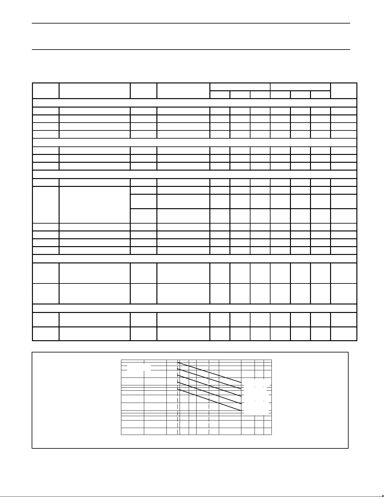
DC AND AC ELECTRICAL CHARACTERISTICS
V
CC
= 12V, specifications apply over temperature, unless otherwise specified.
TEST
SE5562 NE5562
SYMBOL
PARAMETER
TEST
PINS
TEST CONDITIONS
Min Typ Max Min Typ Max
UNIT
Internal reference
V
REF
Reference voltage Internal TA=25°C 3.76 3.80 3.84 3.76 3.80 3.84 V
V
REF
Reference voltage Internal Over temp. 3.72 3.8 3.90 3.725 3.8 3.870 V
Temperature stability Internal 30 30 ppm/°C
Long-term stability Internal 0.5 0.5
µV/1000
hrs
Philips Semiconductors Product specification
NE/SE5562Switched-mode power supply control circuit
1994 Aug 31
4
DC AND AC ELECTRICAL CHARACTERISTICS (Continued)
V
CC
= 12V, specifications apply over temperature, unless otherwise specified.
TEST
SE5562 NE5562
SYMBOL
PARAMETER
TEST
PINS
TEST CONDITIONS
Min Typ Max Min Typ Max
UNIT
Reference
V
Z
Zener voltage 9
IL=7mA,
T
A
=25°C
7.35 7.60 7.75 7.35 7.6 7.75 V
V
Z
Zener voltage 9
IL=7mA,
Over temp.
7.25 7.80 7.20 7.78 V
∆VZ/ ∆T Temperature stability 9 IL<1mA 50 50 ppm/°C
Low supply shutdown
Comparator threshold
voltage
Internal TA=25°C 8.30 8.45 8.75 8.30 8.45 8.75 V
Comparator threshold
voltage
Internal Over temp. 8.00 8.45 8.90 8.00 8.45 8.90 V
Hysteresis Internal 25 50 8.00 25 50 800 mV
Oscillator
f
MIN
Frequency range,
minimum
1, 2,
3, 11
RT=42.7kΩ,
C
T
=0.47µF
60 80 60 80 Hz
f
MAX
Frequency range,
maximum
1, 2,
3, 11
RT=2.87kΩ,
C
T
=380pF
600 600 kHz
Initial accuracy
1, 2,
3, 11
fO=52kHz,
R
T
=16kΩ
and C
T
=0.0015µF,
T
A
=25°C
48.6 54 59.4 48.6 54 59.4 kHz
Voltage stability
1, 2, 3,
11, 17
10V<VS<18V -215 -215 ppm/V
Temperature stability
1, 2,
3, 11
300 500 300 500 ppm/°C
Sawtooth peak voltage 2, 3 TA=25°C
1
5.00 5.25 5.40 5.00 5.25 5.40 V
2, 3 Over temp. 4.80 5.25 5.60 4.80 5.25 5.60 V
Sawtooth valley voltage 2, 3 TA=25°C 1.25 1.70 2.00 1.25 1.70 2.00 V
2, 3 Over temp. 1.0 1.7 2.1 1.25 1.7 2.0 V
Sync. in high level 11 2.0 V
Z
2.0 V
Z
V
Sync. in low level 11 0.0 0.8 0.0 0.8 V
Sync. in bias current 11
(Sourced),
V
11
<0.8V
0.50 10.0 0.50 10.0 µA
Feed-forward ratio,
maximum
1 2 2
Feed-forward duty cycle
reduction
1
VFF=2VZ,
T
A
=25°C
11 13.5 19 11 13.5 19 %
1 Over temp. 6 13.5 22 8 22 %
Feed-forward reference
voltage
9 V
Z
V
S
V
Z
V
S
V
Feed-forward bias current 1 2.5 50.0 2.5 50.0 µA
Philips Semiconductors Product specification
NE/SE5562Switched-mode power supply control circuit
1994 Aug 31
5
DC AND AC ELECTRICAL CHARACTERISTICS (Continued)
V
CC
= 12V, specifications apply over temperature, unless otherwise specified.
TEST
SE5562 NE5562
SYMBOL
PARAMETER
TEST
PINS
TEST CONDITIONS
Min Typ Max Min Typ Max
UNIT
Error amp
I
BIAS
Input bias current 8 1.0 5.0 1.0 5.0 µA
A
VOL
DC open-loop gain 8, 10 RL>100kΩ 60 86 60 86 dB
V
OH
High output voltage 10 I
SOURCE
=1mA 5 5 V
V
OL
Low output voltage 10 I
SINK
=1mA 2.0 2.0 V
PSRR from VZ and V
S
Internal fO<300kHz -40 -40 dB
BW
Small-signal gain bandwidth
product
8 8 MHz
Feedback resistor range 1 240 1 240 kΩ
I
SINK
Output sink current V8=V10=5V 10 10 mA
I
SOURCE
Output source current
V8=3V,
V10=1V
5 5 mA
Sawtooth feedthrough
AV=100,
0% duty cycle
200 200 mV
PWM comparator and modulator
Minimum duty cycle 19
@V
COMP
<,
f=300kHz
0 0 %
Maximum duty cycle 19
@V
COMP
>,
f=300kHz,
V15=0V
95 98 95 98 %
A
CC
Duty cycle 10, 19
f=15kHz to
200kHz,
V
IN
=0.472 V
Z
41 49 55 41 49 55 %
t
PD
Propagation delay to
output
2, 19 V15=0 400 400 ns
I
BIAS
Bias current, external
modulator input
4 (Sourced) 0.20 20 0.20 20 µA
I
BIAS
Bias current, duty cycle
control
5 (Sourced) 0.20 20 0.20 20 µA
Soft-start trip voltage 5 .910 0.955 0.990 0.922 0.955 0.988 V
Remote on/off (shutdown)
Output enabled 6 0 0.80 0 0.80 V
Output disabled 6 2 V
Z
2 V
Z
V
I
BIAS
Bias current 6 1 10 1 10 µA
V
IN
Maximum input voltage 6 V
Z
V
Z
V
Delay to output(s) 6, 19 400 400 ns
Current limit comparator(s)
Shutdown, OC2 14 .593 0.645 .697 0.593 0.645 0.697 V
Minimum duty cycle, OC1 14 .486 0.528 .570 0.486 0.528 0.570 V
I
BIAS
Bias current 14 (Sourced) 0.5 50 0.5 50 µA
OC
1
C
DELAY
charge current 16 -18.2 -13 -6.5 -18.2 -13 -7.8 µA
OC2 C
DELAY
charge current 16 -770 -550 -250 -770 -550 -330 µA
C
DELAY
Discharge current 16 V12=V
Z
0.4 1.4 4.0 0.8 1.4 2.0 µA
C
DELAY
Shut off trip level 16 TA=25°C 3.75 3.86 3.97 3.75 3.86 3.97 V
Philips Semiconductors Product specification
NE/SE5562Switched-mode power supply control circuit
1994 Aug 31
6
DC AND AC ELECTRICAL CHARACTERISTICS (Continued)
V
CC
= 12V, specifications apply over temperature, unless otherwise specified.
TEST
SE5562 NE5562
SYMBOL
PARAMETER
TEST
PINS
TEST CONDITIONS
Min Typ Max Min Typ Max
UNIT
Auxiliary comparator with shutdown
I
BIAS
Bias current 12 (Sourced) 1 10 1 10 µA
Threshold voltage 12 3.69 3.80 3.91 3.69 3.80 3.91 V
C
DELAY
Discharge current 12 VIN=3V 5 10 5 10 mA
Hysteresis 12, 13 10 10 mV
Demagnetization overvoltage comparator
I
BIAS
Bias current 18 2 10 2 10 µA
Threshold voltage 18 3.62 3.80 3.91 3.69 3.80 3.91 V
Hysteresis 18 10 10 mV
Output stage
V
OH
High output voltage 19 I
SOURCE
=100mA VS-2.5 VS-1.9 VS-2.5 VS-1.9 V
19 I
SINK
=2mA 0.16 0.4 0.16 0.4 V
19
I
SINK
=100mA,
T
A
=25°C
1.4 2.0 1.4 2.0 V
OL
19
I
SINK
=100mA,
over temp.
2.25 2.25 V
I
SINK
max 19 100 100 mA
I
SOURCE
max 19 100 100 mA
t
R
Rise time 19 CL=2000pF 160 160 ns
t
F
Fall time 19 CL=2000pF 80 80 ns
Supply current/voltage
I
CC
Supply current 17
10V<VS<16V
(Voltage-fed mode),
V
I<VS
9 15 9 15 mA
V
S
Input voltage 7, 17
II=15mA,
(Current-fed mode)
V
S
=meter
14.2 15.3 16.7 14.2 15.3 16.7 V
Operating frequency range for all functions but feed-forward working cycle-by-cycle
f
MIN
Minimum frequency All
RT=42.7kΩ,
C
T
=0.47µF
60 80 60 80 Hz
f
MAX
Maximum frequency All
RT=2.87kΩ,
C
T
=380pF
600 1000 600 1000 kHz
FREQUENCY (kHz)
10
3
10
2
10
1
10
0
10
2
5 x 1021035 x 10
3
10
4
CT (pF)
TA = 25°C
RT = 2.5kΩ
RT = 5kΩ
RT = 10kΩ
RT = 20kΩ
RT = 40kΩ
SL00390
Figure 3. Frequency vs RT, CT NE/SE5562
V
OL
Low output voltage
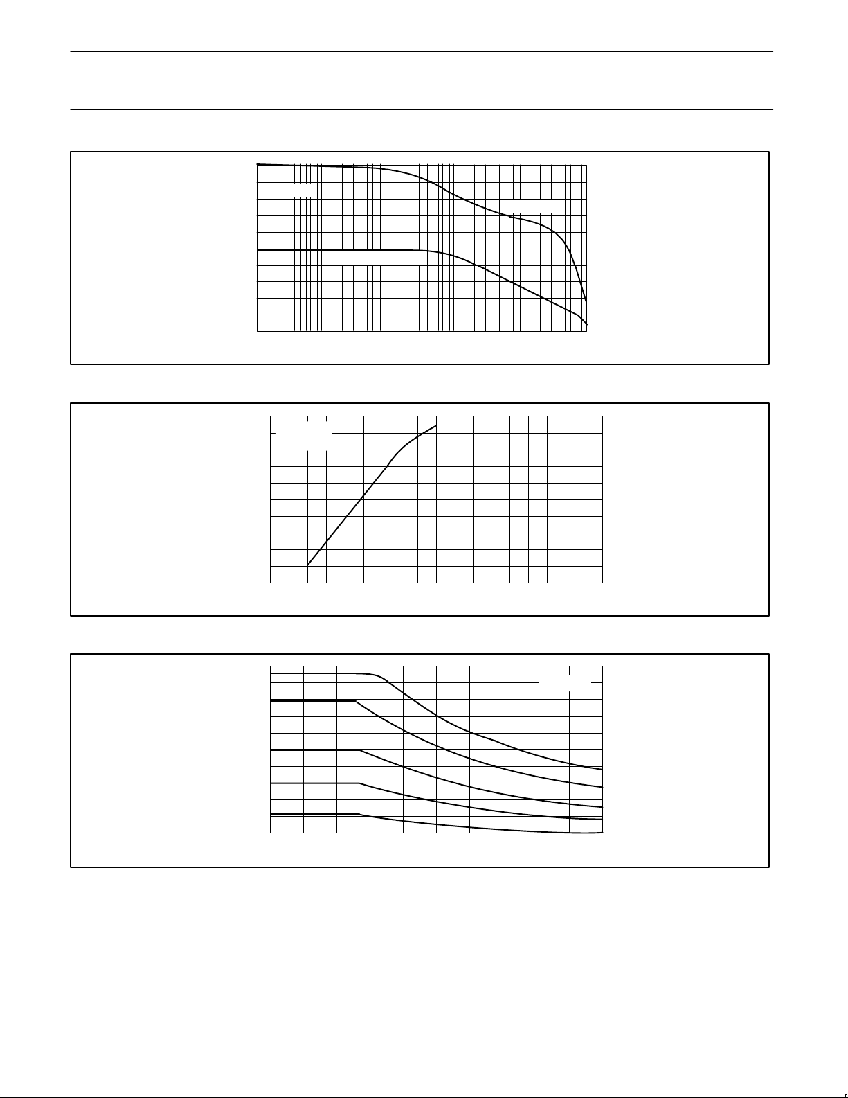
Philips Semiconductors Product specification
NE/SE5562Switched-mode power supply control circuit
1994 Aug 31
7
40
30
20
10
0
100
1k 10k 100k 1M
10M
GAIN (dB)
0
–30
–60
–90
–120
–150
–180
PHASE (DEG)
FREQUENCY
TA = 25°C
CLOSED-LOOP GAIN
PHASE
SL00391
Figure 4. Error Amplifier Closed-Loop Response
PWM INPUT VOLTAGE (V)
100
90
80
70
60
50
40
30
20
10
0
1 2 3 4 5 6 7 8 9 10
DUTY CYCLE (%)
VCC = 12V
TA = 25°C
SL00392
Figure 5. Duty Cycle vs PWM Input Voltage
FEED-FORWARD VOLTAGE (V)
TA = 25°C
DUTY CYCLE (%)
100
90
80
70
60
50
40
30
20
10
0
5 6 7 8 9 10 11 12 13 14 15
SL00393
Figure 6. Duty Cycle vs Feed-forward Voltage
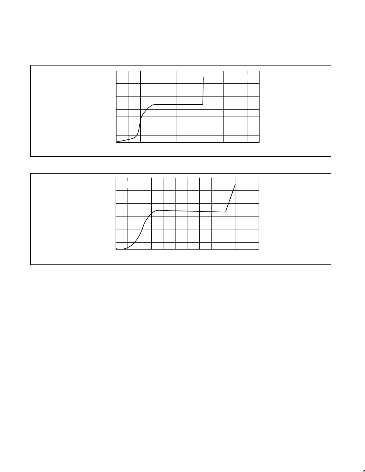
Philips Semiconductors Product specification
NE/SE5562Switched-mode power supply control circuit
1994 Aug 31
8
SUPPLY VOLTAGE (PIN 17)(V)
SUPPLY CURRENT (PIN 17) (mA)
22
20
18
16
14
12
10
8
6
4
2
0
0 2 4 6 8 10 12 14 16 18 20 22 24
TA = 25°C
SL00394
Figure 7. Current-Feed Characteristics
SUPPLY VOLTAGE (PIN 17)(V)
SUPPLY CURRENT (PIN 17) (mA)
22
20
18
16
14
12
10
8
6
4
2
0
0 2 4 6 8 10 12 14 16 18 20 22 24
TA = 25°C
SL00395
Figure 8. Voltage-Feed Characteristics
Philips Semiconductors Product specification
NE/SE5562Switched-mode power supply control circuit
1994 Aug 31
9
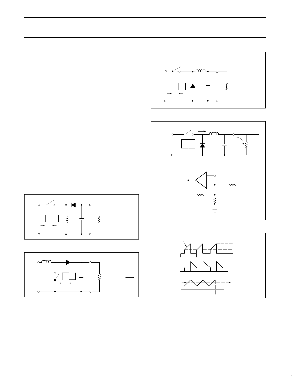
THE NE/SE5562 THEORY OF OPERATION
INTRODUCTION
Switched-mode power conversion relies on the principle of pulsed
energy storage in an inductive or capacitive element. Capacitive
switched converters are typically used with low power systems for
which only tens of milliamperes are required. Medium and high
power converters tend to use inductive storage elements as shown
in Figures 9-11 with which a single switch may be moved around to
create step-up (flyback) positive or negative polarity and step-down
(forward or buck) conversion from a fixed-voltage source. The
relationship between input and output voltage in each case is
controlled by the switching on-to-off ratios, which is termed duty
cycle. Duty cycle modulation is the common factor in this basic type
of power control mechanism. By adding a high-gain operational
amplifier, having one input tied to a stable DC reference voltage,
configured in a negative feedback loop to maintain a constant output
voltage as shown in Figure 12, the switched-mode controller
becomes a dynamic voltage regulator. It is this single-switch
topology that is most readily adapted to the NE/SE5562 SMPS
Control IC.
The ability to switch inductor currents at rates up to 600kHz with
state-of-the-art power FETs makes the design of small, efficient
switching power converters an attainable reality. Protective features
such as programmable slow-start and cycle-by-cycle current limiting
allow safe, maintenance-free power supplies to be mass-produced
at reduced cost to the manufacturer. Integrated technology makes
long-term reliability a predictably achievable goal.
V
OUT
V
IN
1
R
L
D
O
SW
V
IN
L
C
O
δ
–
+
COM
SL00396
Figure 9. Negative Output Flyback Converter
V
OUT
V
IN
1
R
L
D
O
SW
V
IN
L
C
O
δ
–
+
COM
+
SL00397
Figure 10. Positive Output Flyback Converter
WHERE
tSWON
T
PERIOD
V
OUT
V
IN
R
L
D
B
SW
V
IN
L
C
O
δ
–
+
COM
+
SL00398
Figure 11. Forward Converter (Single Inductor) Step Down
PWM
L
C
REGULATED
OUTPUT
A
+
–
V
IN
UNREGULATED
DC
V
REF
I
SW
I
L
R
L
R
F
R
2
R
1
+
–
+
–
SL00399
Figure 12. The Forward (Buck) Converter (V
OUT
= VIN(δ))
i
t
E
L
SWITCH
CURRENT
DIODE
CURRENT
TOTAL
INDUCTOR
CURRENT
MAGNETIZATION
CURRENT
LOAD CURRENT
AVERAGE
INDUCTOR
CURRENT
SL00400
Figure 13. PWM Switching Waveforms
 Loading...