

Philips NE531N, NE531FE, SE531FE Datasheet
Philips Semiconductors Linear Products Product specification
NE/SE531High slew rate operational amplifier
70
August 31, 1994 853-0809 13721
DESCRIPTION
The 531 is a fast slewing high performance operational amplifier
which retains DC performance equal to the best general purpose
types while providing far superior large-signal AC performance. A
unique input stage design allows the amplifier to have a large-signal
response nearly identical to its small-signal response. The amplifier
is compensated for truly negligible overshoot with a single capacitor.
In applications where fast settling and superior large-signal
bandwidths are required, the amplifier out-performs conventional
designs which have much better small-signal response. Also,
because the small-signal response is not extended, no special
precautions need be taken with circuit board layout to achieve
stability. The high gain, simple compensation, and excellent stability
of this amplifier allow its use in a wide variety of instrumentation
applications.
FEATURES
•35V/µs slew rate at unity gain
•Pin-for-pin replacement for µA709, µA748, or LM101
•Compensated with a single capacitor
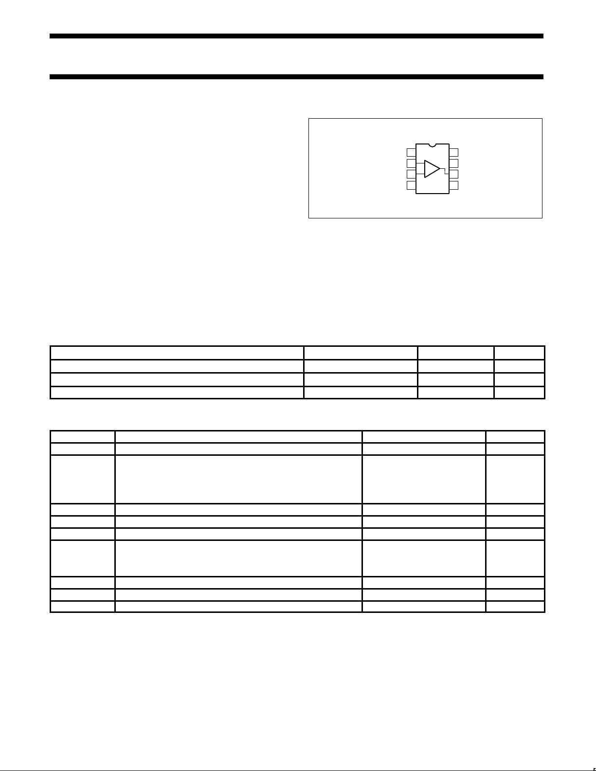
PIN CONFIGURATIONS
1
2
3
4 5
6
7
8
–
+
OFFSET NULL
INVERTING INPUT
NON–INVERTING INPUT
V–
FREQ. COMP.
V+
OUTPUT
OFFSET
N, FE Packages
•Same low drift offset null circuitry as µA741
•Small-signal bandwidth 1MHz
•Large-signal bandwidth 500kHz
•True op amp DC characteristics make the 531 the ideal answer to
all slew rate limited operational amplifier applications
ORDERING INFORMATION
DESCRIPTION TEMPERATURE RANGE ORDER CODE DWG #
8-Pin Plastic Dual In-Line Package (DIP) 0 to +70°C NE531N 0404B
8-Pin Ceramic Dual In-Line Package (CERDIP) -55°C to +125°C SE531FE 0580A
8-Pin Ceramic Dual In-Line Package (CERDIP) 0°C to +70°C NE531FE 0580A
ABSOLUTE MAXIMUM RATINGS
SYMBOL PARAMETER RATING UNIT
V
S
Supply voltage ±22 V
P
D MAX
Maximum power dissipation
TA=25°C (still-air)
1
FE package 780 mW
N package 1160 mW
Differential input voltage ±15 V
V
CM
Common-mode input voltage
2
±15 V
Voltage between offset null and V- ±0.5 V
T
A
Operating ambient temperature range
NE531 0 to +70 °C
SE531 -55 to +125 °C
T
STG
Storage temperature range -65 to +150 °C
T
SOLD
Lead soldering temperature (10sec max) 300 °C
Output short-circuit duration
3
indefinite
NOTES:
1. The following derating factors should be applied above 25°C:
FE package at 6.2mW/°C
N package at 9.3mW/°C
2. For supply voltages less than ±15V, the absolute maximum input voltage is equal to the supply voltage.
3. Short-circuit may be to ground or either supply. Rating applies to +125°C case temperature or to +75°C ambient temperature.

Philips Semiconductors Linear Products Product specification
NE/SE531High slew rate operational amplifier
August 31, 1994
71
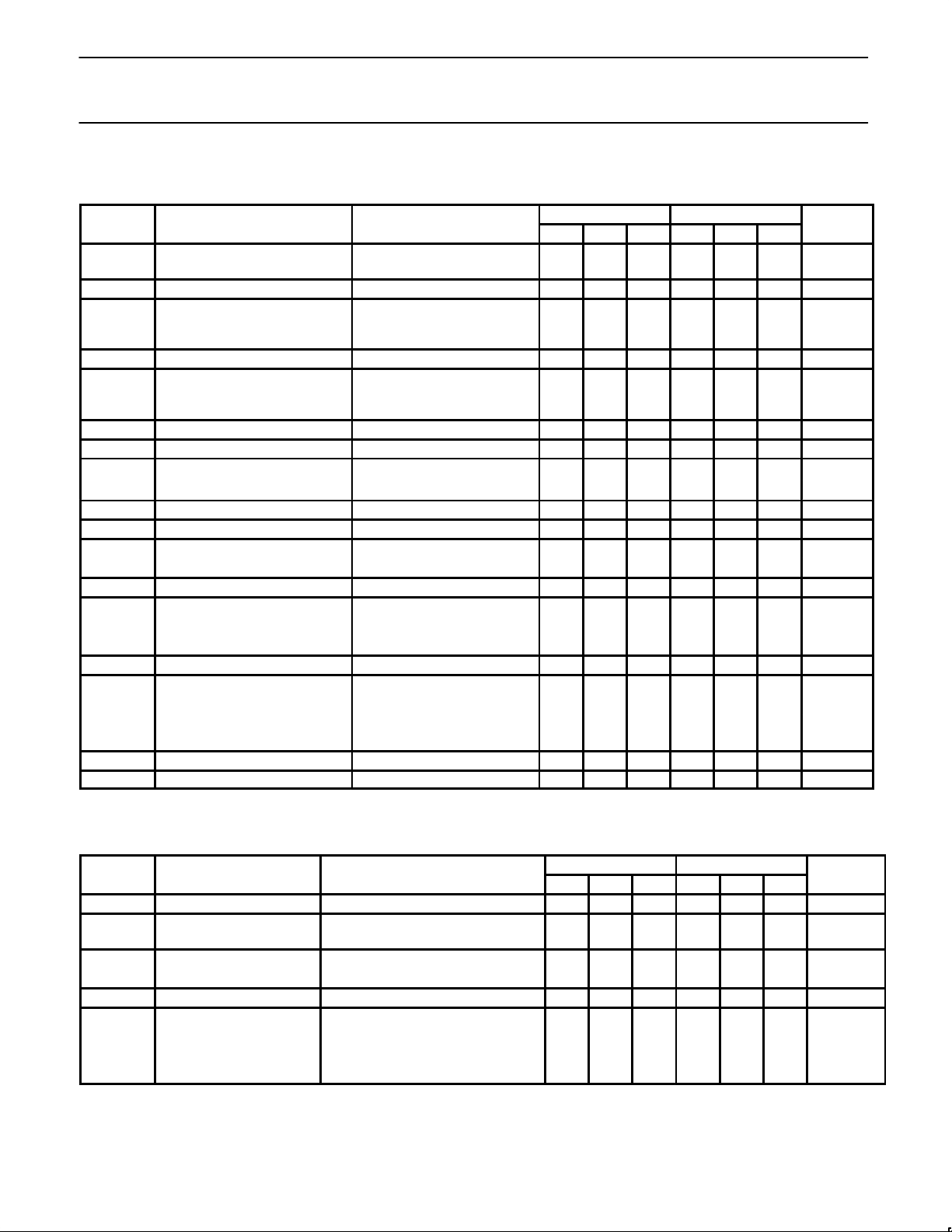
EQUIVALENT SCHEMATIC
INPUT
2
Q1
Q2
R1
Q3
R2
.2
R3
2.2
Q7
Q9
Q10
R8
2.2
Q6
R5
.2
Q5
Q6
R4
R15
100
Q20
Q19
R14
10
R20
.33
Q23
Q27
Q38
Q37
Q29
Q22
Q35
Q21
R16
10
Q11 Q12
R18
.33
Q28
Q25
R24
.04
OUTPUT
R22
3.3
R28
.04
Q30
Q32
Q31
R17
10
Q33
Q34
Q24
Q23
R10
6.5
R21
.2
R27
6.5
R13
1.6
5 6
OFFSET ADJUST
FREQUENCY
COMPENSATION
Q13 Q14
Q15
R7
6.5
R11
1.5
R8
7.8
R12
.17
Q17
Q18
Q19
R9
1.8
INPUT
3
+
OFFSET
ADJUST
1
4
V
R10
6.5
q8
Philips Semiconductors Linear Products Product specification
NE/SE531High slew rate operational amplifier
August 31, 1994
72
DC ELECTRICAL CHARACTERISTICS
VS=±15V, unless otherwise specified.
SE531 NE531
SYMBOL
PARAMETER
TEST CONDITIONS
Min Typ Max Min Typ Max
UNIT
V
OS
Offset voltage
RS≤10kΩ, TA=25°C
R
S
310kΩ, over temp
2.0 5.0
6.0
2.0 6.0
7.5
mV
mV
∆V
OS
Over temp 10 10 µV/°C
I
OS
Offset current
TA=25°C
T
A
=High
T
A
=Low
30 200
200
500
50 200
200
300
nA
nA
nA
∆I
OS
Over temp 0.4 0.4 nA/°C
I
BIAS
Input bias current
T=25°C
T
A
=High
T
A
=Low
300 500
500
1500
400 1500
1500
2000
nA
nA
nA
∆I
BIAS
Over temp 2 2 nA/°C
V
CM
Common-mode voltage range TA=25°C ±10 ±10 V
CMRR Common-mode rejection ratio
TA=25°C, RS≤10kΩ
70 100 dB
Over temp RS≤10kΩ 70 90 dB
R
IN
Input resistance TA=25°C 20 20 MΩ
V
OUT
Output voltage swing RL≥10kΩ, over temp ±10 ±13 ±10 ±13 V
I
CC
Supply current TA=25°C 7.0 10 mA
T
MAX
7.0 10 mA
P
D
Power consumption TA=25°C 210 300 mW
RS≤10kΩ, TA=25°C 10 150 µV/V
PSRR Power supply rejection ratio
RS≤10kΩ, over temp 10 150 µV/V
R
OUT
Output resistance TA=25°C 75 75 Ω
TA=25°C,
R
L
≥10kΩ, V
OUT
=±10V
50 100 20 60 V/mV
A
VOL
Large-signal voltage gain
RL≥10kΩ, V
OUT
=±10V,
over temp
25 15 V/mV
V
INN
Input noise voltage 25°C f=1kHz 20 20 nV/√Hz
I
SC
Short-circuit current 25°C 5 15 45 5 15 45 mA
AC ELECTRICAL CHARACTERISTICS
TA=25°C VS=+15V, unless otherwise specified.
1
SE531 NE531
SYMBOL
PARAMETER
TEST CONDITIONS
Min Typ Max Min Typ Max
UNIT
BW Full power bandwidth 500 500 kHz
t
S
Settling time (1%)
(0.1%)
AV=+1, VIN=±10V
1.5
2.5
1.5
2.5
µs
µs
Large-signal overshoot AV=+1, VIN=±10V 2 2 %
Small-signal overshoot AV=+1, VIN=400mV 5 5 %
t
R
Small-signal rise time AV=+1, VIN=400mV 300 300 ns
SR Slew rate AV=100 35 35 V/µs
AV=10 35 35 V/µs
AV=1 (non-inverting) 20 30 30 V/µs
AV=1 (inverting) 25 35 35 V/µs
NOTES:
1. All AC testing is performed in the transient response test circuit.
 Loading...