

Philips SAA7335GP Datasheet

INTEGRATED CIRCUITS
DATA SH EET
SAA7335
DSP for CD and DVD-ROM
systems
Preliminary specification
Supersedes data of 1997 Aug 11
File under Integrated Circuits, IC01
2001 apr 05
Philips Semiconductors Preliminary specification
DSP for CD and DVD-ROM systems SAA7335
FEATURES
• Compatibility with CD-I, CD-ROM, MPEG-video
DVD-ROM and DVD-video applications
• Designed for very high playback speeds
• Typical CD-ROM operation up to n = 12, DVD-ROM to
n = 1.9, maximum rates (tbf)
• Matched filtering, quad-pass error correction
(C1-C2-C1-C2), overspeed audio playback function
included (up to 3 kbytes buffer)
• Lock-to-disc playback, Constant Angular Velocity
(CAV),pseudo-ConstantLinearVelocity(CLV)andCLV
motor control loops
• Interface to 32 kbytes SRAM for DVD error correction
and de-interleave
• Sub-code/ header processing for DVD and CD formats
• Programmable HF equalizer
• In DVD mode it is still compatible with Philips block
decoders
• Sub-CPU interface can be parallel or fast I2C-bus
• On-chip clock multiplier.
GENERAL DESCRIPTION
This device is a high-end combined Compact Disc (CD)
and Digital Versatile Disc (DVD) compatible decoding
device. The device operates with an external 32 kbytes
S-RAMmemoryforde-interleavingoperations.Thedevice
provides quad-pass error correction for CD-ROM
applications (C1-C2-C1-C2) and operates in lock-to-disk,
CAV, pseudo CLV and CLV modes.
InDVDmodes double-pass C1-C2 error correction is used
which is capable of correcting up to 5 C1 frame errors and
16 C2 frame errors.
The SAA7335 contains all the functions required to
decode an EFM or EFM+ HF signal directly from the laser
pre-amplifier, including analog front-end, PLL data
recovery, demodulation and error correction. The spindle
motor interface provides both motor control signals from
the demodulator and, in addition, contains a tachometer
loop that accepts tachometer pulses from the motor unit.
The SAA7335 has two independent microcontroller
interfaces. The first is a serial I2C-bus and the second is a
standard 8-bit multiplexed parallel interface. Both of these
interfaces provide access to a total of 32 × 8-bit registers
for control and status.
This data sheet contains an descriptive overview of the
device together with electrical and timing characteristics.
For a detailed description of the device refer to the user
guide
“SAU/UM96018”
.
Supply of this CD/DVD IC does not convey an implied
license under any patent right to use this IC in any CD or
DVD application.
QUICK REFERENCE DATA
SYMBOL PARAMETER MIN. TYP. MAX. UNIT
V
I
DDD
V
I
DDA
f
xtal
T
T
DDD
DDA
amb
stg
digital supply voltage 4.5 5.0 5.5 V
digital supply current − 70 300 mA
analog supply voltage 4.5 5.0 5.5 V
analog supply current − 70 300 mA
crystal input frequency 4 25 tbf MHz
operating ambient temperature −20 − +70 °C
storage temperature −55 − +125 °C
2001 apr 05 2
Philips Semiconductors Preliminary specification
DSP for CD and DVD-ROM systems SAA7335
ORDERING INFORMATION
TYPE
NUMBER
NAME DESCRIPTION VERSION
PACKAGE
SAA7335GP LQFP100 plastic low profile quad flat package; 100 leads; body 14 × 14 × 1.4 mm SOT407-1
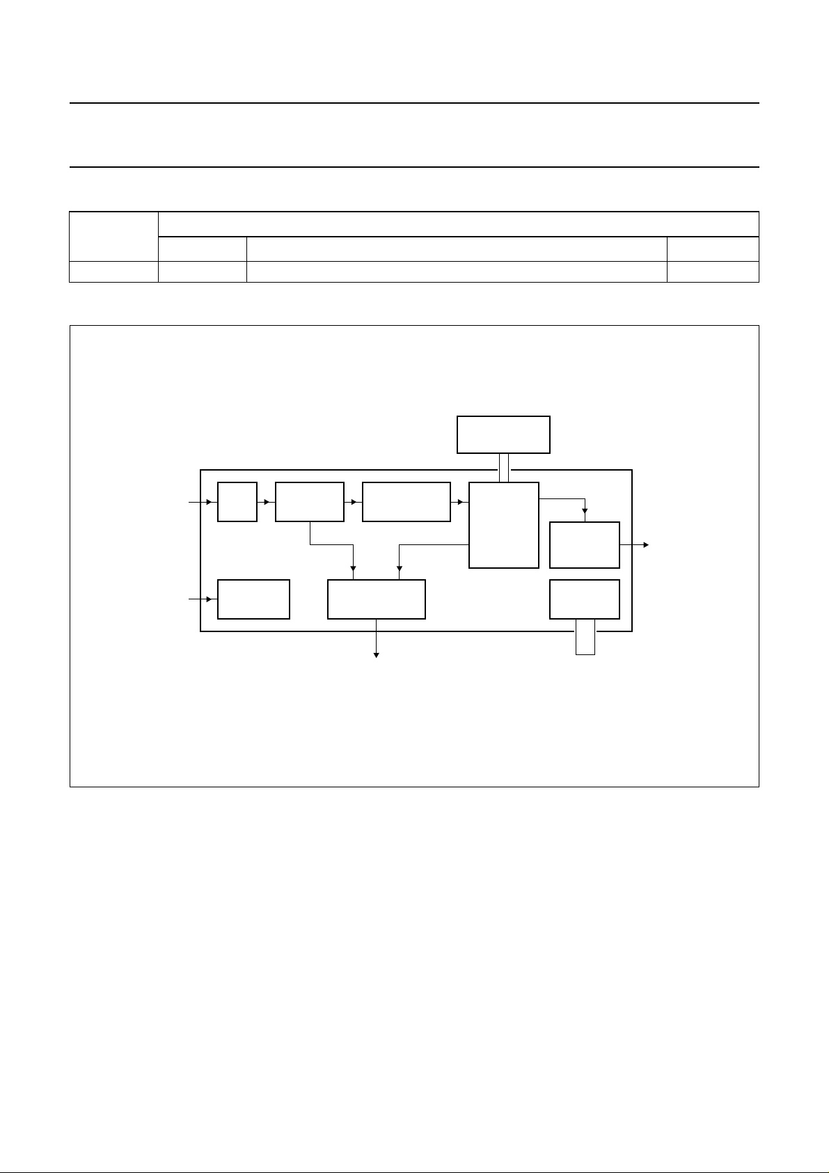
BLOCK DIAGRAM
handbook, full pagewidth
clock input
ADCHF input
CLOCK
GENERATOR
PLL BIT
DETECTOR
DEMODULATOR
EFM/EFM+
SPINDLE
MOTOR CONTROL
SRAM
32 KBYTES
DECODER
SAA7335
I2S-BUS
OUTPUT
INTERFACE
SUB-CPU
INTERFACE
block
decoder
output
motor control
Fig.1 Simplified block diagram.
MGK242
2001 apr 05 3

Philips Semiconductors Preliminary specification
DSP for CD and DVD-ROM systems SAA7335
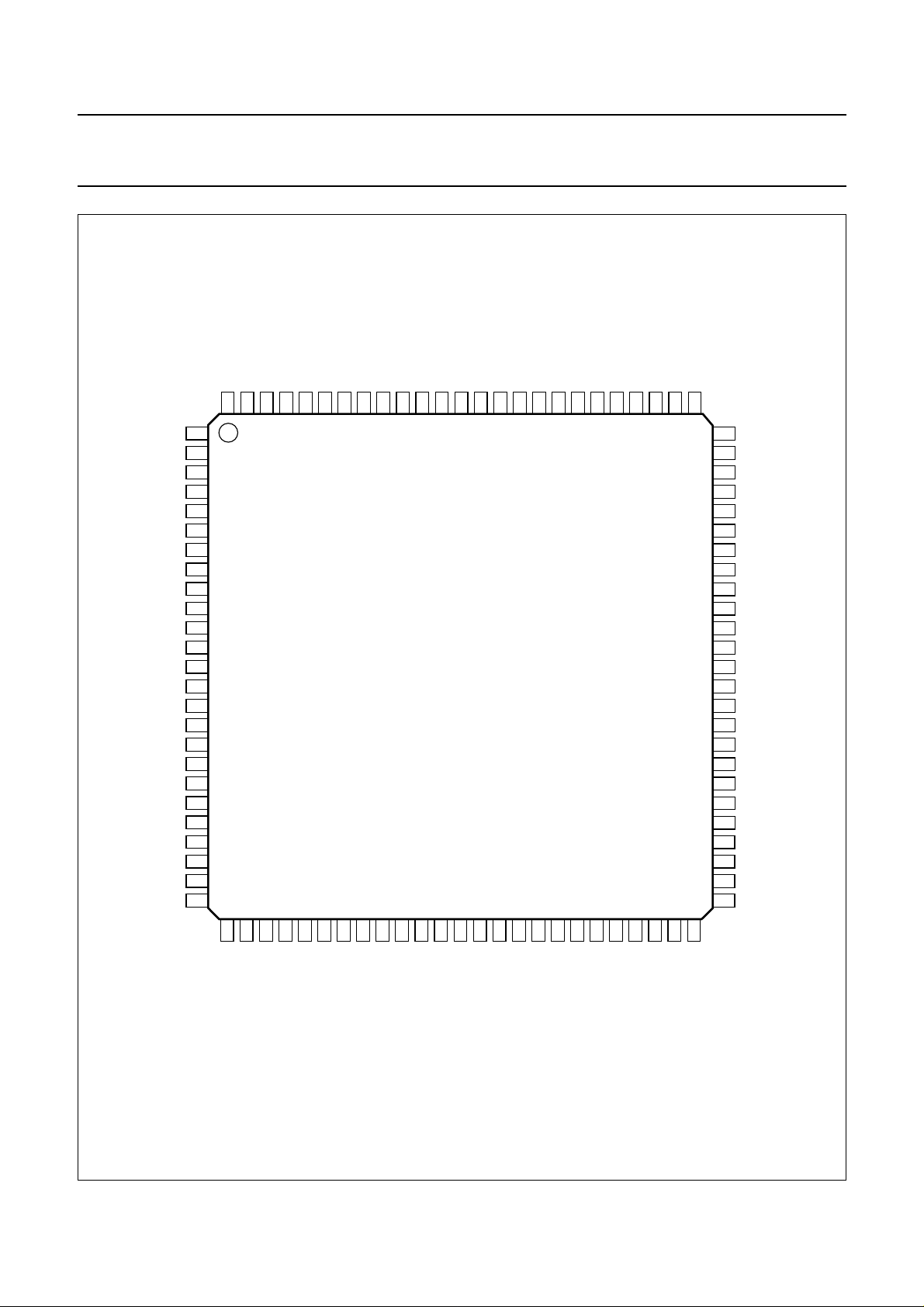
PINNING
SYMBOL PIN TYPE DESCRIPTION
V
SSA1
I
ref
REFLo 3 I analog low reference input for ADC
REFHi 4 I analog high reference input for ADC
VREF 5 I analog negative input
HFIN 6 I analog positive input
V
SSA2
AGCOUT 8 O analog test pin output
V
DDA2
V
DDD1
V
SSD1
OTD 12 I off track detect input
MOTO1 13 O 3-state motor control output
n.c. 14 − not connected, reserved
MOTO2/T3 15 I/O motor control output/tachometer 3 input
n.c. 16 − not connected, reserved
T1 17 I tachometer 1 input
T2 18 I tachometer 2 input
V
DDD2
V
SSD2
TEST1 21 I test input 1
TEST2 22 I test input 2
POR 23 I power-on reset input
MUXSWICH 24 I use clock multiplier input
n.c. 25 − not connected, reserved
CL1 26 O divided clock output
BCAIN 27 I BCA input
SDA 28 I/O sub-CPU I
SCL 29 I sub-CPU I
INT 30 O sub-CPU interrupt output (open-drain)
V
DDD3
V
SSD3
da7 33 I/O sub-CPU data bus bit 7 input/output (parallel)
da6 34 I/O sub-CPU data bus bit 6 input/output (parallel)
da5 35 I/O sub-CPU data bus bit 5 input/output (parallel)
n.c. 36 − not connected, reserved
da4 37 I/O sub-CPU data bus bit 4 input/output (parallel)
n.c. 38 − not connected, reserved
da3 39 I/O sub-CPU data bus bit 3 input/output (parallel)
da2 40 I/O sub-CPU data bus bit 2 input/output (parallel)
1 supply analog ground 1
2 I analog current reference input for ADC
7 supply analog ground 2
9 supply analog supply voltage 2
10 supply digital supply voltage 1
11 supply digital ground 1
19 supply digital supply voltage 2
20 supply digital ground 2
2
C-bus serial data input/output
2
C-bus serial clock input
31 supply digital supply voltage 3
32 supply digital ground 3
2001 apr 05 4
Philips Semiconductors Preliminary specification
DSP for CD and DVD-ROM systems SAA7335
SYMBOL PIN TYPE DESCRIPTION
da1 41 I/O sub-CPU data bus bit 1 input/output (parallel)
n.c. 42 − not connected, reserved
da0 43 I/O sub-CPU data bus bit 0 input/output (parallel)
V
DDD4
V
SSD4
WRi 46 I sub-CPU write enable input (active LOW)
RDi 47 I sub-CPU read enable input (active LOW)
ALE 48 I sub-CPU address latch enable input
CSi 49 I sub-CPU chip select input (active HIGH)
STOPCLOCK 50 O stop clock output
n.c. 51 − not connected, reserved
V4 52 O serial subcode output (for CD)
EBUOUT 53 O digital audio output
SYNC 54 O I
FLAG 55 O I
DATA 56 O I
BCLK 57 I/O I
WCLK 58 I/O I
V
DDD5
V
SSD5
RAMRW 61 O RAM read/write control output
n.c. 62 − not connected, reserved
RAMDA7 63 I/O RAM data bus bit 7 input/output
RAMDA6 64 I/O RAM data bus bit 6 input/output
RAMDA5 65 I/O RAM data bus bit 5 input/output
RAMDA4 66 I/O RAM data bus bit 4 input/output
RAMDA3 67 I/O RAM data bus bit 3 input/output
RAMDA2 68 I/O RAM data bus bit 2 input/output
n.c. 69 − not connected, reserved
RAMDA1 70 I/O RAM data bus bit 1 input/output
RAMDA0 71 I/O RAM data bus bit 0 input/output
V
DDD6
V
SSD6
RAMAD0 74 O RAM address bit 0 output
RAMAD1 75 O RAM address bit 1 output
RAMAD2 76 O RAM address bit 2 output
RAMAD3 77 O RAM address bit 3 output
RAMAD4 78 O RAM address bit 4 output
RAMAD5 79 O RAM address bit 5 output
RAMAD6 80 O RAM address bit 6 output
V
DDD7
44 supply digital supply voltage 4
45 supply digital ground 4
2
S-bus sector sync output
2
S-bus correction flag output
2
S-bus serial data output
2
S-bus bit serial clock input/output
2
S-bus word clock input/output
59 supply digital supply voltage 5
60 supply digital ground 5
72 supply digital supply voltage 6
73 supply digital ground 6
81 supply digital supply voltage 7
2001 apr 05 5

Philips Semiconductors Preliminary specification
DSP for CD and DVD-ROM systems SAA7335
SYMBOL PIN TYPE DESCRIPTION
V
SSD7
RAMAD7 83 O RAM address bit 7 output
RAMAD8 84 O RAM address bit 8 output
RAMAD9 85 O RAM address bit 9 output
n.c. 86 − not connected, reserved
RAMAD10 87 O RAM address bit 10 output
RAMAD11 88 O RAM address bit 11 output
RAMAD12 89 O RAM address bit 12 output
RAMAD13 90 O RAM address bit 13 output
RAMAD14 91 O RAM address bit 14 output
V
DDD8
V
SSD8
CRIN 94 I analog crystal input
CROUT 95 O analog crystal output
CFLG 96 O correction statistics output
MEAS1 97 O front-end telemetry output
V
DDD9
V
SSD9
V
DDA1
82 supply digital ground 7
92 supply digital supply voltage 8
93 supply digital ground 8
98 supply digital supply voltage 9
99 supply digital ground 9
100 supply analog supply voltage 1
2001 apr 05 6
Philips Semiconductors Preliminary specification
DSP for CD and DVD-ROM systems SAA7335
handbook, full pagewidth
V
SSA1
I
ref
REFLo
REFHi
VREF
HFIN
V
SSA2
AGCOUT
V
DDA2
V
DDD1
V
SSD1
OTD
MOTO1
n.c.
MOTO2/T3
n.c.
T1
T2
V
DDD2
V
SSD2
TEST1
TEST2
POR
MUXSWICH
n.c.
1
2
3
4
5
6
7
8
9
10
11
12
13
14
15
16
17
18
19
20
21
22
23
24
25
DDA1VSSD9VDDD9
V
100
MEAS1
CFLG
99989796959493929190898887868584838281
CROUT
CRIN
SSD8VDDD8
V
RAMAD14
RAMAD13
RAMAD12
RAMAD11
RAMAD10
n.c.
RAMAD9
RAMAD8
SAA7335
SSD7VDDD7
RAMAD7
V
RAMAD6
RAMAD5
RAMAD4
RAMAD3
8079787776
RAMAD2
75
74
73
72
71
70
69
68
67
66
65
64
63
62
61
60
59
58
57
56
55
54
53
52
51
RAMAD1
RAMAD0
V
SSD6
V
DDD6
RAMDA0
RAMDA1
n.c.
RAMDA2
RAMDA3
RAMDA4
RAMDA5
RAMDA6
RAMDA7
n.c.
RAMRW
V
SSD5
V
DDD5
WCLK
BCLK
DATA
FLAG
SYNC
EBUOUT
V4
n.c.
26
CL1
SDA
BCAIN
31323334353637383940414243444546474849
SCL
INT
DDD3
V
SSD3
V
da7
da6
da5
n.c.
da4
30
29
28
27
Fig.2 Pin configuration.
2001 apr 05 7
n.c.
da3
da2
da1
n.c.
da0
DDD4
V
SSD4
V
WRi
RDi
ALE
50
CSi
STOPCLOCK
MGK241

Philips Semiconductors Preliminary specification
DSP for CD and DVD-ROM systems SAA7335
FUNCTIONAL DESCRIPTION
Analog front-end
ThisblockconvertstheHFinputtothe digital domain using
an 8-bit ADC proceeded by an AGC circuit to obtain the
optimum performance from the convertor. This block is
clocked by ADCCLK which is set by the external crystal
frequency plus a flexible clock multiplier and divider block.
PLL and bit detector
This subsystem recovers the data from the channel
stream. The block corrects asymmetry, performs noise
filtering and equalisation and finally recovers the bit clock
and data from the channel using a digital PLL.
The equalizer and the data slicer are programmable.
Digital logic
All the digital system logic is clocked from the master ADC
clock (ADCCLK) described above.
Advanced bit detector
The advanced bit detector offers improved data recovery
for multi-layer discs and contains two extra detection
circuits to increase the margins in the bit recovery block:
1. Adaptive slicer: adds a second stage slicer with higher
bandwidth
2. Runlength 2 push-back: all T2 runlengths are pushed
back to T3, thereby automatically determining the
erroneous edge and shifting the transitions on that
edge.
Demodulator
FRAME SYNC PROTECTION CD MODE
This circuit detects the frame synchronization signals.
Two synchronization counters are used in the SAA7335:
1. The coincidence counter: this is used to detect the
coincidence of successive syncs. It generates a sync
coincidence signal if 2 syncs are 588 ±1 EFM clocks
apart.
2. The main counter: this is used to partition the EFM
signal into 17-bit words. This counter is reset when:
a) A sync coincidence is generated
b) A sync is found within ±6 EFM clocks of its
expected position.
The sync coincidence signal is also used to generate the
lock signal which will go active HIGH when 1 sync
coincidence is found. It will reset to LOW when, during
61 consecutive frames, no sync coincidence is found.
FRAME SYNC PROTECTION DVD MODE
This circuit detects the frame synchronization signals.
Two synchronization counters are used in the SAA7335:
1. The coincidence counter: this is used to detect the
coincidence of successive syncs. It generates a sync
coincidence signal if 2 syncs are 1488 ±3 EFM+
clocks apart.
2. The main counter: this is used to partition the EFM+
signal into 16-bit words. This counter is reset when:
a) A sync coincidence is generated
b) A sync is found within ±10 EFM+ clocks of its
expected position.
The sync coincidence signal is also used to generate the
lock signal which will go active HIGH when 1 sync
coincidence is found. It will reset to LOW when, during
61 consecutive frames, no sync coincidence is found.
EFM/EFM+ demodulation
The 14-bit EFM (16-bit EFM+) data and subcode words
are decoded into 8-bit symbols.
2001 apr 05 8

Philips Semiconductors Preliminary specification
DSP for CD and DVD-ROM systems SAA7335
Microcontroller interface
The SAA7335 has two microcontroller interfaces, one
serial I2C-bus and one parallel (8051 microcontroller
compatible).
The two communication modes may be operated at the
same time, the modes are described below:
1. Parallel mode: protocol compatible with 8052
multiplexed bus:
a) da0 to da7 = address/data bus
b) ALE = Address Latch Enable, latches the address
information on the bus
c) WRi = active LOW write signal for write to
SAA7335
d) RDi = active LOW read signal for read from
SAA7335
e) CSi = active HIGH Chip Select signal (this signal
gates the RDi and WRi signals).
2. I2C-bus mode: I2C-bus protocol where SAA7335
behaves as slave device where:
a) SDA = I2C-bus data
b) SCL = I2C-bus clock
c) I2C-bus slave address (write mode) = 3EH
d) I2C-bus slave address (read mode) = 3FH
e) Maximum data transfer rate = 400 kbits/s.
ICROCONTROLLER INTERFACE (I
M
2
C-BUS MODE)
Thesequenceforawritedatacommand(1 data byte) is as
follows:
• Send START condition
• Send address 3EH (write)
• Write command address byte
• Write data byte
• Send STOP condition.
Thesequence for a read data command(that reads 1 data
byte) is as follows:
• Send START condition
• Send address 3EH (write)
• Write status address byte
• Send STOP condition
• Send START condition
• Send address 3FH (read)
• Read data byte
• Send STOP condition.
R
EADING AND WRITING DATA TO THE SAA7335
The SAA7335 has 32 × 8-bit configuration and status
registers as shown in Table 1. Not all locations are
currently defined and some remain reserved for future
upgrades. These can be written to or read from via the
microcontroller interface using either the serial or parallel
control bus.
Bytes are transferred over the interface in single bytes of
which there are two types; write data commands and read
data commands.
2001 apr 05 9
This text is here in white to force landscape pages to be rotated correctly when browsing through the pdf in the Acrobat reader.This text is here in
_white to force landscape pages to be rotated correctly when browsing through the pdf in the Acrobat reader.This text is here inThis text is here in
white to force landscape pages to be rotated correctly when browsing through the pdf in the Acrobat reader. white to force landscape pages to be ...
2001 apr 05 10
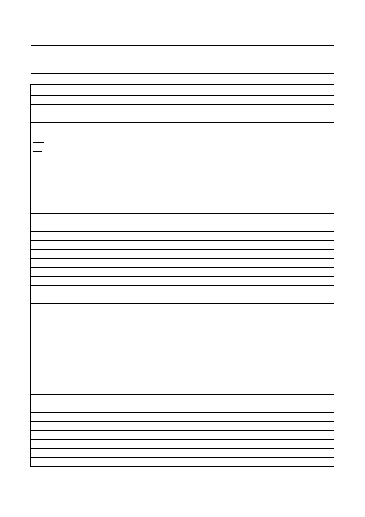
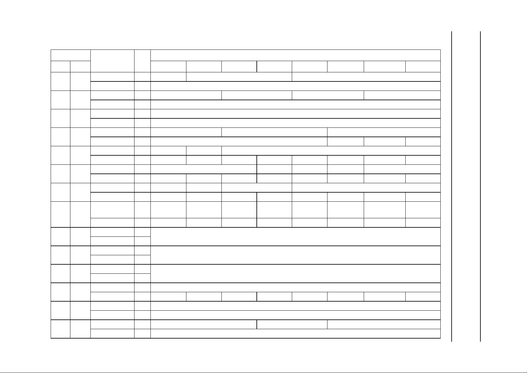
REGISTER MAP
Table 1 SAA7335 microcontroller register map
ADDRESS
DEC HEX 7 6 5 4 3 2 1 0
0 0 PLL_LOCK W Lock Oride Pha_Oset PLL_Force_L
1 1 PLL_SET W SliceBW Integ_F0 PLLBW_F1 LP_BW_F3
2 2 PLL_FREQ W PLL frequency (8 MSBs)
3 3 PLL_EQU W PLL frequency (2 LSBs) equalizer tap α 1 equaliser tap α 2
4 4 PLL_F_MEAS W RL3_EN reserved EFM nominal setting (101110)
5 5 OUTPUT1 W Fmat(3 to 1) WCLK_Op BCLK_Op Fmat (0) SyncSwap (1 and 0)
6 6 OUTPUT2 W EBU_Valid EBU_On EBU control bits 28, 29 EBU control bits (1 to 4)
7 7 OUTPUT3 W WCLK_H_
8 8 SEMA1 W general purpose semaphore register
9 9 SEMA2 W general purpose semaphore register
10 A SEMA3 W general purpose semaphore register
11 B INTEN W hardware pin interrupt enable bits (map to status bits)
12 C MOTOR1 W frequency set point
13 D MOTOR2 W G(2 to 0) Ki Kf
NAME R/W
PLL_Freq_R R PLL measured frequency (bits 9 to 2)
PLL_ASSYM R PLL asymmetry value (8 bits)
PLL_Jit R jitter value (bits 9 to 2)
PLL_Lock_In R reserved Long_Symb F_Lock In_Lock
reserved R −−−−−− − −
reserved R −−−−−− − −
reserved R −−−−−− − −
Descr_On Interp_On CD_ROM_
Left
reserved R −−−−−− − −
R
R
R
Status R Fl_S1 Fl_S2 Fl_S3 PLL lock DVD rdy Mot Ov Tacho reserved
SLICE1 R slice compensation value
EYE_Open R eye opening value
Header_On
BIT
Flag_Pin Kill Data On Kill EBU_On CD_ROM_
Philips Semiconductors Preliminary specification
DSP for CD and DVD-ROM systems SAA7335
Scrb_On
This text is here in white to force landscape pages to be rotated correctly when browsing through the pdf in the Acrobat reader.This text is here in
_white to force landscape pages to be rotated correctly when browsing through the pdf in the Acrobat reader.This text is here inThis text is here in
white to force landscape pages to be rotated correctly when browsing through the pdf in the Acrobat reader. white to force landscape pages to be ...
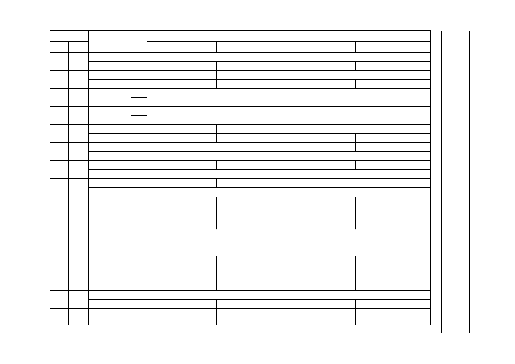
2001 apr 05 11
ADDRESS
DEC HEX 7 6 5 4 3 2 1 0
14 E MOTOR3 W FIFO set point
15 F MOTO4 W PWM_PDM OVF_SW SW2 SW1 motor servo control (3 to 0)
16 10 MTR_INTG_L W motor integrator value (7 to 0)
17 11 MTR_INTG_H W motor integrator value (15 to 8)
18 12 CLOCKPRE W CL1Div BCLKG_En Div1 (2 to 0) Mux 2 Div2 (2 to 0)
19 13 DECMODE W mode reserved read TOC reserved
20 14 reserved W −−−−−− − −
21 15 ANASET W AGC_En gain set gain up gain down AGC_On reserved
22 16 VITSET W slice ON AdDet ON FEndAutoS
23 17 TACHO1 W tachometer multiplier frequency KTacho (7 to 0)
24 18 TACHO2 W tachometer interrupt trip frequency tachometer trip (7 to 0)
25 19 TACHO3 W servo control source Tacho
26 1A BCASET W BCA_Freq (7 to 0)
27 to311B to
1F
NAME R/W
MTR_F R −−−−−− − −
reserved R −−−−−− − −
R
R
SUB_C_STAT R ready busy CRC_OK err (2 to 0) cor fail reserved
SUB_C_DATA R subcode data (7 to 0)
SUB_C_End R no meaning (register read used as a signal)
FIFOFILL_L R number of C1 frames in FIFO
ON
BCA_STAT R Buff_
Loaded
BCA_DATA R BCA data (7 to 0)
reserved R −−−−−− − −
reserved R −−−−−− − −
reserved R −−−−−− − −
reserved −−−−−− − −
sync Buff_ORun
Moto2_T3 Fsam TachoInt_LF reserved
FRes
BIT
Philips Semiconductors Preliminary specification
DSP for CD and DVD-ROM systems SAA7335
 Loading...