

Philips SAA7325H-M1 Datasheet
DATA SH EET
Product specification
File under Integrated Circuits, IC01
1999 Jun 17
INTEGRATED CIRCUITS
SAA7325
Digital servo processor and
Compact Disc decoder with
integrated DAC (CD10)

1999 Jun 17 2
Philips Semiconductors Product specification
Digital servo processor and Compact Disc
decoder with integrated DAC (CD10)
SAA7325
CONTENTS
1 FEATURES
2 GENERAL DESCRIPTION
3 ORDERING INFORMATION
4 QUICK REFERENCE DATA
5 BLOCK DIAGRAM
6 PINNING
7 FUNCTIONAL DESCRIPTION
7.1 Decoder part
7.1.1 Principal operational modes of the decoder
7.1.2 Decoding speed and crystal frequency
7.1.3 Lock-to-disc mode
7.1.4 Standby modes
7.2 Crystal oscillator
7.3 Data slicer and clock regenerator
7.4 Demodulator
7.4.1 Frame sync protection
7.4.2 EFM demodulation
7.5 Subcode data processing
7.5.1 Q-channel processing
7.5.2 EIAJ 3 and 4-wire subcode (CD graphics)
interfaces
7.5.3 V4 subcode interface
7.6 FIFO and error corrector
7.6.1 Flags output (CFLG)
7.7 Audio functions
7.7.1 De-emphasis and phase linearity
7.7.2 Digital oversampling filter
7.7.3 Concealment
7.7.4 Mute, full-scale, attenuation and fade
7.7.5 Peak detector
7.8 DAC interface
7.8.1 Internal bitstream digital-to-analog converter
(DAC)
7.8.2 External DAC interface
7.9 EBU interface
7.9.1 Format
7.10 KILL circuit
7.11 Audio features off
7.12 The VIA interface
7.13 Spindle motor control
7.13.1 Motor output modes
7.13.2 Spindle motor operating modes
7.13.3 Loop characteristics
7.13.4 FIFO overflow
7.14 Servo part
7.14.1 Diode signal processing
7.14.2 Signal conditioning
7.14.3 Focus servo system
7.14.4 Radial servo system
7.14.5 Off-track counting
7.14.6 Defect detection
7.14.7 Off-track detection
7.14.8 High-level features
7.14.9 Driver interface
7.14.10 Laser interface
7.14.11 Radial shock detector
7.15 Microcontroller interface
7.15.1 Microcontroller interface (4-wire bus mode)
7.15.2 Microcontroller interface (I2C-bus mode)
7.15.3 Decoder registers and shadow registers
7.15.4 Summary of functions controlled by decoder
registers 0 to F
7.15.5 Summary of functions controlled by shadow
registers
7.15.6 Summary of servo commands
7.15.7 Summary of servo command parameters
8 LIMITING VALUES
9 CHARACTERISTICS
10 OPERATING CHARACTERISTICS
(SUBCODE INTERFACE TIMING)
11 OPERATING CHARACTERISTICS (I2S-BUS
TIMING)
12 OPERATING CHARACTERISTICS
(MICROCONTROLLER INTERFACE TIMING)
13 APPLICATION INFORMATION
14 PACKAGE OUTLINE
15 SOLDERING
15.1 Introduction to soldering surface mount
packages
15.2 Reflow soldering
15.3 Wave soldering
15.4 Manual soldering
15.5 Suitability of surface mount IC packages for
wave and reflow soldering methods
16 DEFINITIONS
17 LIFE SUPPORT APPLICATIONS
18 PURCHASE OF PHILIPS I2C COMPONENTS

1999 Jun 17 3
Philips Semiconductors Product specification
Digital servo processor and Compact Disc
decoder with integrated DAC (CD10)
SAA7325
1 FEATURES
• Single speed operation
• Integrated bitstream DAC with differential outputs,
operating at 96fs with 3rd-order noise shaper; typical
performance of −90 dB signal-to-noise ratio
• Separate serial input and output interfaces allow data
‘loopback’ mode for use of onboard DAC with external
Electronic Shock Absorption (ESA) systems
• Lock-to-disc mode
• Full error correction strategy, t = 2 and e = 4
• Full CD graphics interface
• All standard decoder functions implemented digitally on
chip
• FIFO overflow concealment for rotational shock
resistance
• Digital audio interface (EBU), audio and data
• 2 and 4 times oversampling integrated digital filter,
including f
s
mode
• Audio data peak level detection
• Kill interface for external DAC deactivation during digital
silence
• All SAA737x (CD7) digital servo and high-level functions
• Low focus noise
• Same playability performance as SAA737x (CD7)
• Automatic closed-loop gain control available for focus
and radial loops
• Pulsed sledge support
• Electronic damping of fast radial actuator during long
jump
• Microcontroller loading LOW
• High-level servo control option
• High-level mechanism monitor
• Communication may be via I
2
C-bus or
TDA1301/SAA7345 compatible bus
• On-chip clock multiplier allows the use of 8.4672,
16.9344 or 33.8688 MHz crystals or ceramic
resonators.
2 GENERAL DESCRIPTION
The SAA7325 (CD10) is a single chip combining the
functions of a CD decoder, digital servo and bitstream
DAC. The decoder/servo part is based on the SAA737x
(CD7) and is software compatible with this design. Extra
functions are controlled by use of ‘shadow’ registers
(see Section 7.15.3).
Supply of this Compact Disc IC does not convey an implied
license under any patent right to use this IC in any
Compact Disc application.
3 ORDERING INFORMATION
TYPE
NUMBER
PACKAGE
NAME DESCRIPTION VERSION
SAA7325H QFP64 plastic quad flat package; 64 leads (lead length 1.6 mm);
body 14 × 14 × 2.7 mm
SOT393-1
1999 Jun 17 4
Philips Semiconductors Product specification
Digital servo processor and Compact Disc
decoder with integrated DAC (CD10)
SAA7325
4 QUICK REFERENCE DATA
SYMBOL PARAMETER CONDITIONS MIN. TYP. MAX. UNIT
V
DD
supply voltage 3.0 3.3 3.6 V
I
DD
supply current − 20 − mA
f
xtal
crystal frequency 8 8.4672 35 MHz
T
amb
ambient temperature −10 − +70 °C
T
stg
storage temperature −55 − +125 °C
S/N
DAC
onboard DAC signal-to-noise ratio 1 kHz; 1fs; see
Figs. 38 and 39
−85 −90 − dB
1999 Jun 17 5
Philips Semiconductors Product specification
Digital servo processor and Compact Disc
decoder with integrated DAC (CD10)
SAA7325
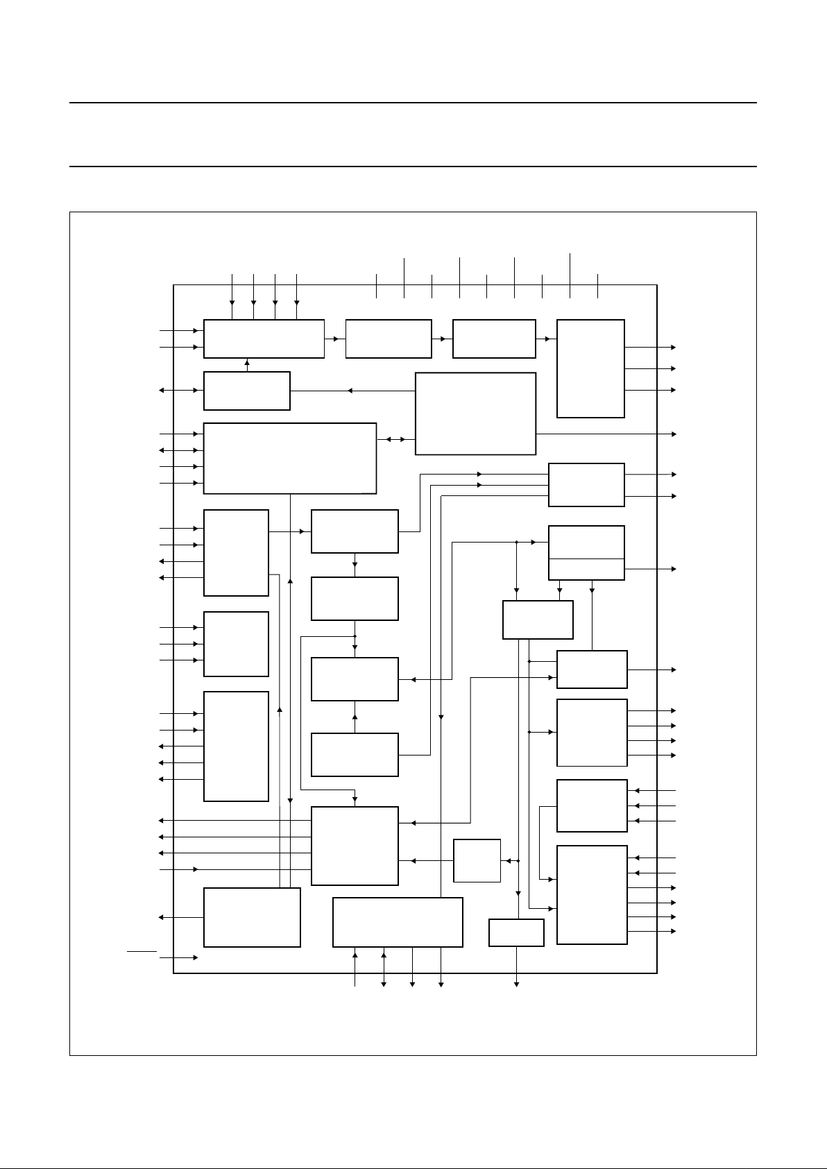
5 BLOCK DIAGRAM
Fig.1 Block diagram.
handbook, full pagewidth
DECODER
MICRO-
CONTROLLER
INTERFACE
VERSATILE PINS
INTERFACE
SUBCODE
PROCESSOR
KILL
PEAK
DETECT
SERIAL DATA
INTERFACE
TIMING
TEST
ADC
V
ref
GENERATOR
FRONT-END
DIGITAL
PLL
MOTOR
CONTROL
AUDIO
PROCESSOR
EBU
INTERFACE
ERROR
CORRECTOR
MICROCONTROLLER
INTERFACE
PRE-
PROCESSING
CONTROL
FUNCTION
CONTROL
PART
EFM
DEMODULATOR
SRAM
RAM
ADDRESSER
OUTPUT
STAGES
FLAGS
12
13
7
40
39
41
42
2
1
3
6
25
31
44
24
16
15
26
49
48
47
46
45
43
38
63 34 61 62 32
8 9 10 11 4 14 5 17 33 50 58 52 57
54
55
56
64
59
60
53
51
30
29
28
27
V
RIN
I
ref
R2
SCL
SDA
RAB
SILD
HFIN
HFREF
ISLICE
TEST1
TEST2
TEST3
SELPLL
CRIN
CROUT
CL16
CL11/4
SBSY
SFSY
SUB
RCK
STATUS
R1
D1 D2 D3 D4
V
SSA1
V
DDA2
V
SSD2
V
DDD2(C)
V
SSA2
V
DDA1
V
SSD1
V
SSD3
V
DDD1(P)
V1 V2/V3 V4 V5 KILL
EF
DATA
WCLK
SCLK
SERIAL DATA
(LOOPBACK)
INTERFACE
37
35
36
SDI
WCLI
SCLI
BITSTREAM
DAC
20
21
18
19
LP
22
RN
23
RP
LN
V
pos
V
neg
DOBM
MOTO2
MOTO1
LDON
SL
FO
RA
CFLG
RESET
SAA7325
MGL681
1999 Jun 17 6
Philips Semiconductors Product specification
Digital servo processor and Compact Disc
decoder with integrated DAC (CD10)
SAA7325
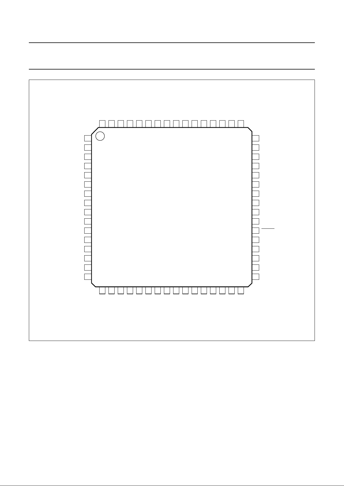
6 PINNING
SYMBOL PIN DESCRIPTION
HFREF 1 comparator common mode input
HFIN 2 comparator signal input
ISLICE 3 current feedback output from data slicer
V
SSA1
4
(1)
analog ground 1
V
DDA1
5
(1)
analog supply voltage 1
I
ref
6 reference current output pin
V
RIN
7 reference voltage for servo ADCs
D1 8 unipolar current input 1 (central diode signal input)
D2 9 unipolar current input 2 (central diode signal input)
D3 10 unipolar current input 3 (central diode signal input)
D4 11 unipolar current input 4 (central diode signal input)
R1 12 unipolar current input 1 (satellite diode signal input)
R2 13 unipolar current input 2 (satellite diode signal input)
V
SSA2
14
(1)
analog ground 2
CROUT 15 crystal/resonator output
CRIN 16 crystal/resonator input
V
DDA2
17
(1)
analog supply voltage 2
LN 18 DAC left channel differential negative output
LP 19 DAC left channel differential positive output
V
neg
20 DAC negative reference input
V
pos
21 DAC positive reference input
RN 22 DAC right channel differential negative output
RP 23 DAC right channel differential positive output
SELPLL 24 selects whether internal clock multiplier PLL is used
TEST1 25 test control input 1 (this pin should be tied LOW)
CL16 26 16.9344 MHz system clock output
DATA 27 serial d4(1) data output (3-state)
WCLK 28 word clock output (3-state)
SCLK 29 serial bit clock output (3-state)
EF 30 C2 error flag output (3-state)
TEST2 31 test control input 2 (this pin should be tied LOW)
KILL 32 kill output (programmable; open-drain)
V
SSD1
33
(1)
digital ground 1
V2/V3 34 versatile I/O: versatile input 2 or versatile output 3 (open-drain)
WCLI 35 word clock input (for data loopback to DAC)
SDI 36 serial data input (for data loopback to DAC)
SCLI 37 serial bit clock input (for data loopback to DAC)
RESET 38 power-on reset input (active LOW)
SDA 39 microcontroller interface data I/O line (open-drain output)
SCL 40 microcontroller interface clock line input
1999 Jun 17 7
Philips Semiconductors Product specification
Digital servo processor and Compact Disc
decoder with integrated DAC (CD10)
SAA7325
Note
1. All supply pins must be connected to the same external power supply voltage.
RAB 41 microcontroller interface R/
W and load control line input (4-wire bus mode)
SILD 42 microcontroller interface
R/W and load control line input (4-wire bus mode)
STATUS 43 servo interrupt request line/decoder status register output (open-drain)
TEST3 44 test control input 3 (this pin should be tied LOW)
RCK 45 subcode clock input
SUB 46 P-to-W subcode bits output (3-state)
SFSY 47 subcode frame sync output (3-state)
SBSY 48 subcode block sync output (3-state)
CL11/4 49 11.2896 or 4.2336 MHz (for microcontroller) clock output
V
SSD2
50
(1)
digital ground 2
DOBM 51 bi-phase mark output (externally buffered; 3-state)
V
DDD1(P)
52
(1)
digital supply voltage 1 for periphery
CFLG 53 correction flag output (open-drain)
RA 54 radial actuator output
FO 55 focus actuator output
SL 56 sledge control output
V
DDD2(C)
57
(1)
digital supply voltage 2 for core
V
SSD3
58
(1)
digital ground 3
MOTO1 59 motor output 1; versatile (3-state)
MOTO2 60 motor output 2; versatile (3-state)
V4 61 versatile output 4
V5 62 versatile output 5
V1 63 versatile input 1
LDON 64 laser drive on output (open-drain)
SYMBOL PIN DESCRIPTION
1999 Jun 17 8
Philips Semiconductors Product specification
Digital servo processor and Compact Disc
decoder with integrated DAC (CD10)
SAA7325
Fig.2 Pin configuration.
handbook, full pagewidth
SAA7325H
MGL693
1
2
3
4
5
6
7
8
9
10
11
12
13
14
15
16
48
47
46
45
44
43
42
41
40
39
38
37
36
35
34
SBSY
SFSY
SUB
RCK
TEST3
STATUS
SILD
RAB
SCL
SDA
SCLI
SDI
WCLI
V2/V3
V
SSD1
HFREF
HFIN
ISLICE
V
SSA1
V
DDA1
I
ref
V
RIN
D1
D2
D3
D4
R1
R2
V
SSA2
CROUT
CRIN 33
17
18
19
20
21
22
23
24
25
26
27
28
29
30
31
32
64
63
62
61
60
59
58
57
56
55
54
53
52
51
50
LDONV1V5
V4
MOTO2
MOTO1
V
SSD3VDDD2(C)
SL
FO
RA
CFLG
V
DDD1(P)
DOBM
V
SSD2
CL11/4
V
DDA2
LN
LP
V
neg
V
pos
RN
RP
SELPLL
TEST1
CL16
DATA
WCLK
SCLK
EF
TEST2
KILL 49
RESET
7 FUNCTIONAL DESCRIPTION
7.1 Decoder part
7.1.1 P
RINCIPAL OPERATIONAL MODES OF THE DECODER
The decoding part supports a full audio specification at
single-speed (n = 1). A simplified data flow through the
decoder part is illustrated in Fig.7.
7.1.2 D
ECODING SPEED AND CRYSTAL FREQUENCY
The SAA7325 is a single-speed decoding device, with an
internal Phase-Locked Loop (PLL) clock multiplier allowing
a choice of different crystals and oscillators to be used
(see Section 7.2). The range of crystal and oscillator
frequencies possible is controlled via decoder register B
and shown in Table 1. The MSB of decoder register B
must be set to logic 0.
The internal clock multiplier is controlled by SELPLL, and
should only be used if a 8.4672 or 16.9344 MHz crystal,
ceramic resonator or external clock is present.

1999 Jun 17 9
Philips Semiconductors Product specification
Digital servo processor and Compact Disc
decoder with integrated DAC (CD10)
SAA7325
7.1.3 LOCK-TO-DISC MODE
Although nominally a single-speed device, for electronic
shock absorption applications the SAA7325 can be put
into lock-to-disc mode. This allows Constant Angular
Velocity (CAV) disc playback with varying input data rates
from the inside-to-outside of the disc. In the lock-to-disc
mode, the FIFO is blocked and the decoder will adjust its
output data rate to the disc speed. Hence, the frequency of
the I2S-bus (WCLK and SCLK) clocks are dependent on
the disc speed. In the lock-to-disc mode there is a limit on
the maximum variation in disc speed that the SAA7325 will
follow. Disc speeds must always be within 25% to 100%
range of their nominal value. The lock-to-disc mode is
enabled/disabled by decoder register E.
7.1.4 S
TANDBY MODES
The SAA7325 may be placed in two standby modes
selected by decoder register B (it should be noted that the
device core is still active):
• Standby 1: ‘CD-STOP’ mode; most I/O functions are
switched off
• Standby 2: ‘CD-PAUSE’ mode; audio output features
are switched off, but the motor loop, the motor output
and the subcode interfaces remain active; this is also
called a ‘Hot Pause’.
In the standby modes the various pins will have the
following values:
• MOTO1 and MOTO2: put in high-impedance, PWM
mode (standby 1 and reset: operating in standby 2); put
in high-impedance, PDM mode (standby 1 and reset:
operating in standby 2)
• SCL and SDA: no interaction; normal operation
continues
• SCLK, WCLK, DATA, EF and DOBM: 3-state in both
standby modes; normal operation continues after reset
• CRIN, CROUT, CL16 and CL11/4: no interaction;
normal operation continues
• V1, V2/V3, V4, V5 and CFLG: no interaction; normal
operation continues.
Table 1 Operating frequencies
Notes
1. The MSB of register B must be held at 0 (i.e. 0XXX).
2. The CL11 output is always a 5.6448 MHz clock if a 16.9344 MHz external clock is used and SELPLL = 0. CL11 is
available on the CL11/4 output, enabled by programming shadow register 3 (see Section 7.15.3).
REGISTER B
(1)
SELPLL
CRYSTAL FREQUENCY (MHz)
CL11 FREQUENCY (MHz)
(2)
33.8688 16.9344 8.4672
00XX 0 √−− 11.2896
00XX 1 −−√ 11.2896
01XX 0 −√− 5.6448
01XX 1 −√− 11.2896
1999 Jun 17 10
Philips Semiconductors Product specification
Digital servo processor and Compact Disc
decoder with integrated DAC (CD10)
SAA7325
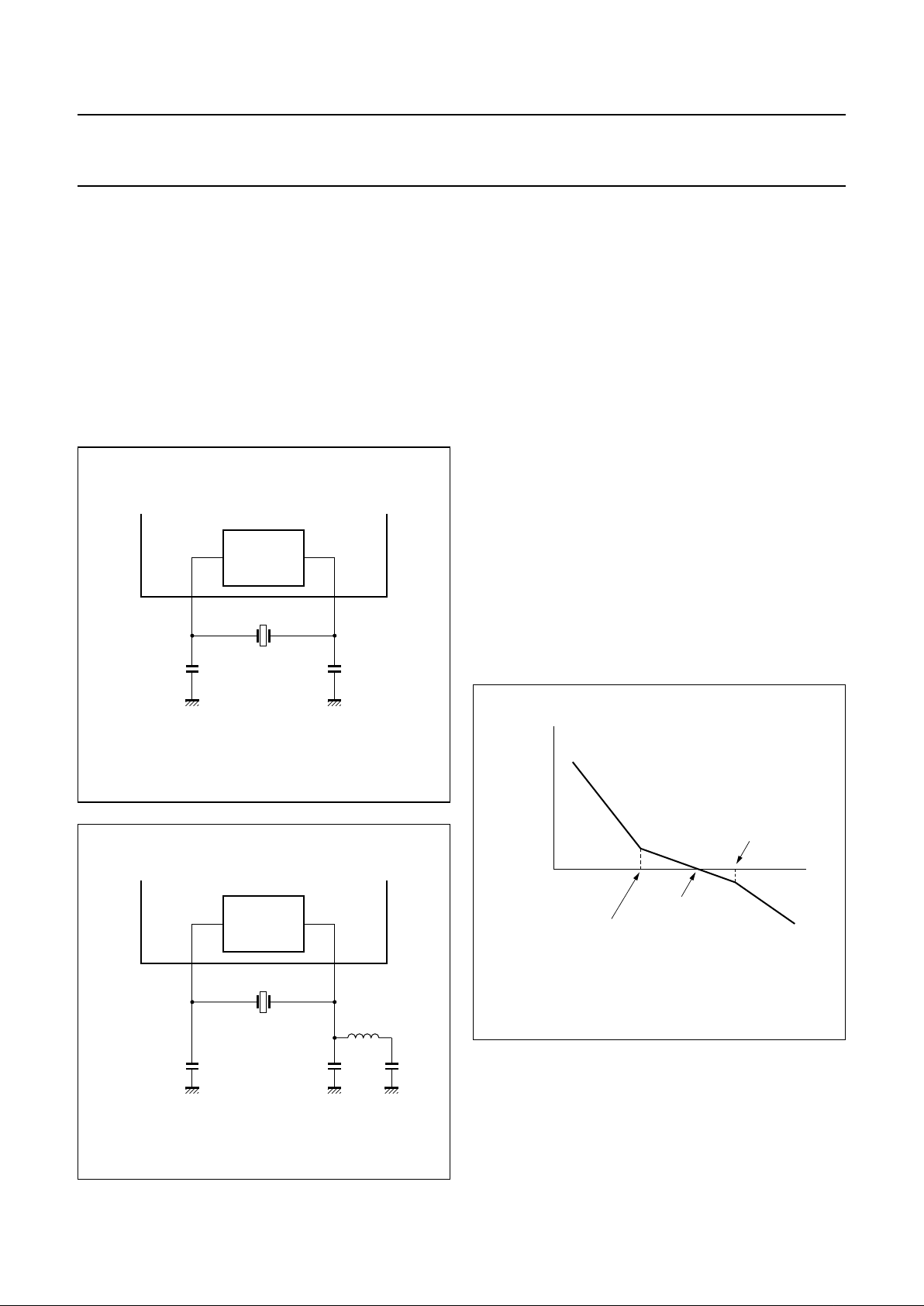
7.2 Crystal oscillator
The crystal oscillator is a conventional 2-pin design
operating between 8 and 35 MHz. This oscillator is
capable of operating with ceramic resonators and with
both fundamental and third overtone crystals. External
components should be used to suppress the fundamental
output of the third overtone crystals as shown in
Figs 3 and 4. Typical oscillation frequencies required are
8.4672, 16.9344 or 33.8688 MHz depending on the
internal clock settings used and whether or not the clock
multiplier is enabled (see Table 1).
Fig.3 8.4672 MHz fundamental configuration.
handbook, halfpage
OSCILLATOR
8.4672 MHz
CRIN
CROUT
SAA7325
33 pF33 pF
MGL694
Fig.4 33.8688 MHz overtone configuration.
handbook, halfpage
OSCILLATOR
33.8688 MHz
CRIN
CROUT
SAA7325
3.3 µH
1 nF10 pF10 pF
MGL695
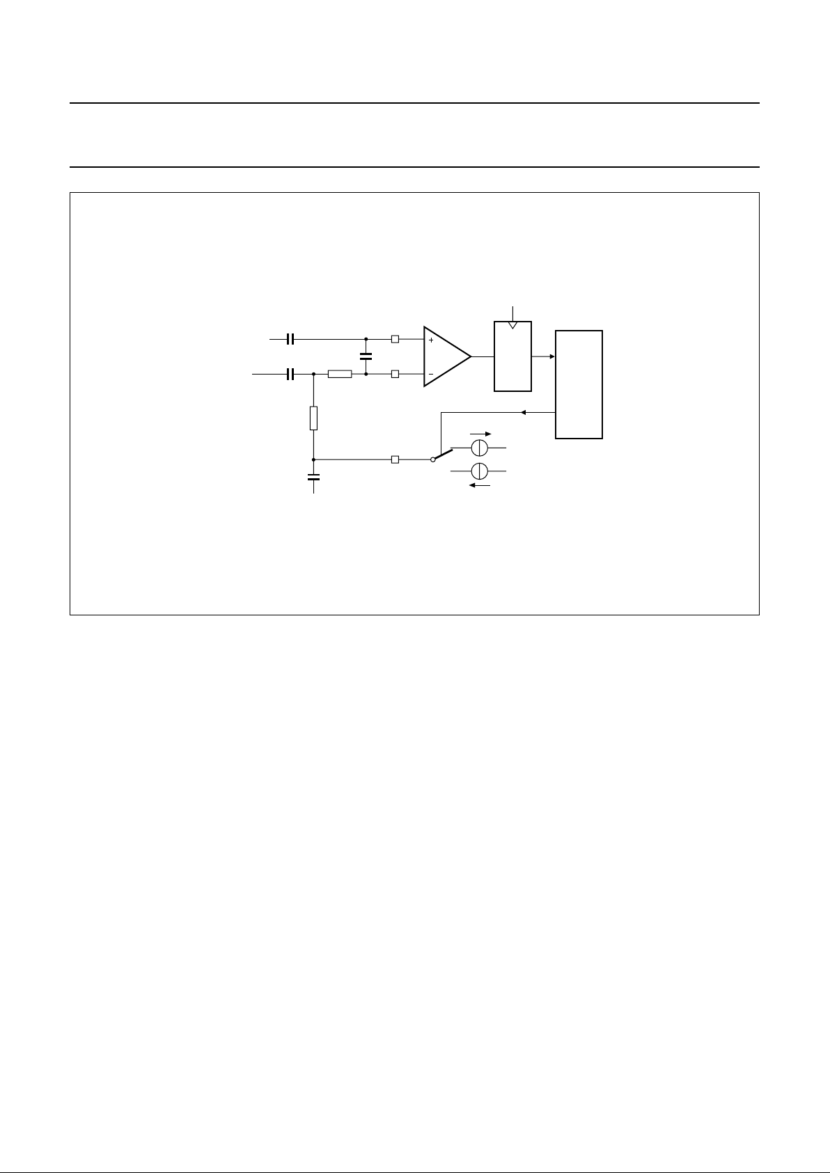
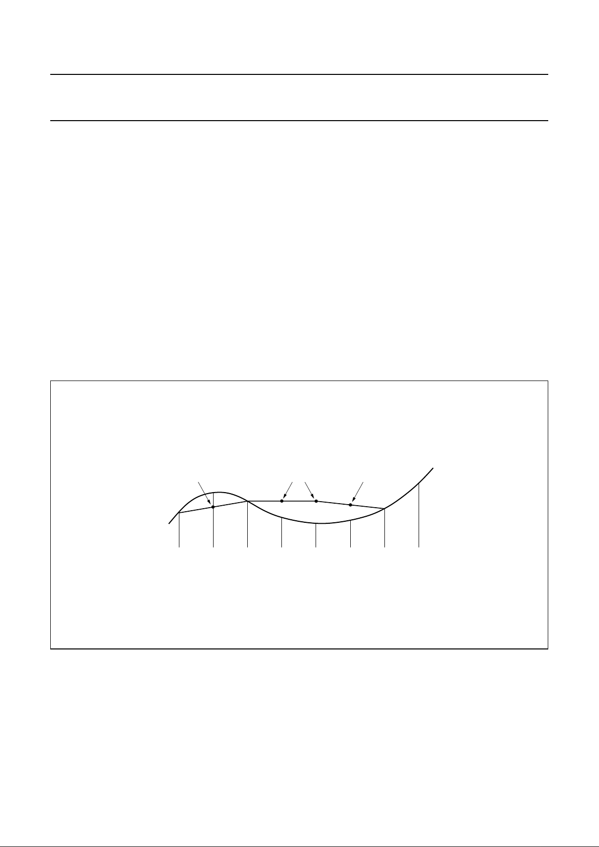
7.3 Data slicer and clock regenerator
The SAA7325 has an integrated slice level comparator
which can be clocked by the crystal frequency clock, or
4 times the crystal frequency clock (if SELPLL is set HIGH
while using a 16.9344 MHz crystal and register 4 is set
to 0XXX), or 8 times the crystal frequency clock
(if SELPLL is set HIGH while using an 8.4672 MHz crystal,
and register 4 is set to 0XXX). The slice level is controlled
by an internal current source applied to an external
capacitor under the control of the Digital Phase-Locked
Loop (DPLL).
Regeneration of the bit clock is achieved with an internal
fully digital PLL. No external components are required and
the bit clock is not output. The PLL has two registers
(8 and 9) for selecting bandwidth and equalization.
The PLL response is shown in Fig.5.
For certain applications an off-track input is necessary.
This is internally connected from the servo part (its polarity
can be changed by the foc_parm1 parameter), but may be
input via the V1 pin if selected by register C. If this flag is
HIGH, the SAA7325 will assume that its servo part is
following on the wrong track, and will flag all incoming HF
data as incorrect.
Fig.5 Digital PLL loop response.
1, 2and 3 are all programmable via decoder register 8.
MGS178
handbook, halfpage
f
3. PLL, LPF
2. PLL bandwidth
1. PLL integrator
PLL
loop
response
1999 Jun 17 11
Philips Semiconductors Product specification
Digital servo processor and Compact Disc
decoder with integrated DAC (CD10)
SAA7325
Fig.6 Data slicer showing typical application components.
47 pF
HFREF
HFIN
ISLICE
22 kΩ
2.2 kΩ
100 nF
100 nF
1 nF
HF input
crystal
clock
DQ
DPLL
V
SSA
V
SSA
V
SS
MGS179
V
DD
100 µA
100 µA
7.4 Demodulator
7.4.1 F
RAME SYNC PROTECTION
A double timing system is used to protect the demodulator
from erroneous sync patterns in the serial data.
The master counter is only reset if:
• A sync coincidence is detected; sync pattern occurs
588 ±1 EFM clocks after the previous sync pattern
• A new sync pattern is detected within ±6 EFM clocks of
its expected position.
The sync coincidence signal is also used to generate the
PLL lock signal, which is active HIGH after 1 sync
coincidence found, and reset LOW if during 61
consecutive frames no sync coincidence is found. The PLL
lock signal can be accessed via the SDA or STATUS pins
selected by decoder registers 2 and 7.
Also incorporated in the demodulator is a Run Length 2
(RL2) correction circuit. Every symbol detected as RL2 will
be pushed back to RL3. To do this, the phase error of both
edges of the RL2 symbol are compared and the correction
is executed at the side with the highest error probability.
7.4.2 EFM
DEMODULATION
The 14-bit EFM data and subcode words are decoded into
8-bit symbols.

1999 Jun 17 12
Philips Semiconductors Product specification
Digital servo processor and Compact Disc
decoder with integrated DAC (CD10)
SAA7325
This text is here in white to force landscape pages to be rotated correctly when browsing through the pdf in the Acrobat reader.This text is here in
_white to force landscape pages to be rotated correctly when browsing through the pdf in the Acrobat reader.This text is here inThis text is here in
white to force landscape pages to be rotated correctly when browsing through the pdf in the Acrobat reader. white to force landscape pages to be ...
Fig.7 Simplified data flow of decoder functions.
k
, full pagewidth
SUBCODE
PROCESSOR
DIGITAL PLL
AND
DEMODULATOR
FIFO
ERROR
CORRECTOR
FADE/MUTE/
INTERPOLATE
DIGITAL
FILTER
PHASE
COMPENSATION
DE-EMPHASIS
FILTER
KILL
1
0
1
0
1
0
1
0
1
0
I2S/EIAJ BUS
INTERFACE
I2S/EIAJ
LOOPBACK
INTERFACE
WCLI
SCLI
SDI
LN
LP
RN
RP
SCLK
WCLK
DATA
EF
decoder
reg 3
V
neg
decoder reg C
decoder reg 3
reg F
decoder reg A
1
0
1: decoder reg 3 ≠ 101X
0: decoder reg 3 = 101X
(CD-ROM modes)
1: shadow reg 7 = XX1X
0: shadow reg 7 = XX0X
1: shadow reg 7 = XX1X
0: shadow reg 7 = XX0X
0: reg D = XX01
1: decoder reg A = XX0X
0: decoder reg A ≠ XX1X
V4 SUBCODE
INTERFACE
MICROCONTROLLER
INTERFACE
CD GRAPHICS
INTERFACE
EBU
INTERFACE
SBSY
SFSY
SUB
RCK
DOBM
V4
SDA
output from
data slicer
1: decoder reg 3 = XX10
(1fs mode)
0: decoder reg 3 ≠ XX10
1: no pre-emphasis detected
OR reg D = 01XX
(de-emphasis signal at V5)
0: pre-emphasis detected
AND reg D ≠ 01XX
KILL
V3
MGS180
1
0
ONBOARD
DAC
1: shadow reg 7 = XXX1
0: shadow reg 7 = XXX0
1
0
1
0
1999 Jun 17 13
Philips Semiconductors Product specification
Digital servo processor and Compact Disc
decoder with integrated DAC (CD10)
SAA7325
7.5 Subcode data processing
7.5.1 Q-
CHANNEL PROCESSING
The 96-bit Q-channel word is accumulated in an internal
buffer. The last 16 bits are used internally to perform a
Cyclic Redundancy Check (CRC). If the data is good, the
SUBQREADY-I signal will go LOW. SUBQREADY-I can
be read via the SDA or STATUS pins, selected via decoder
register 2. Good Q-channel data may be read from SDA.
7.5.2 EIAJ 3
AND 4-WIRE SUBCODE (CD GRAPHICS)
INTERFACES
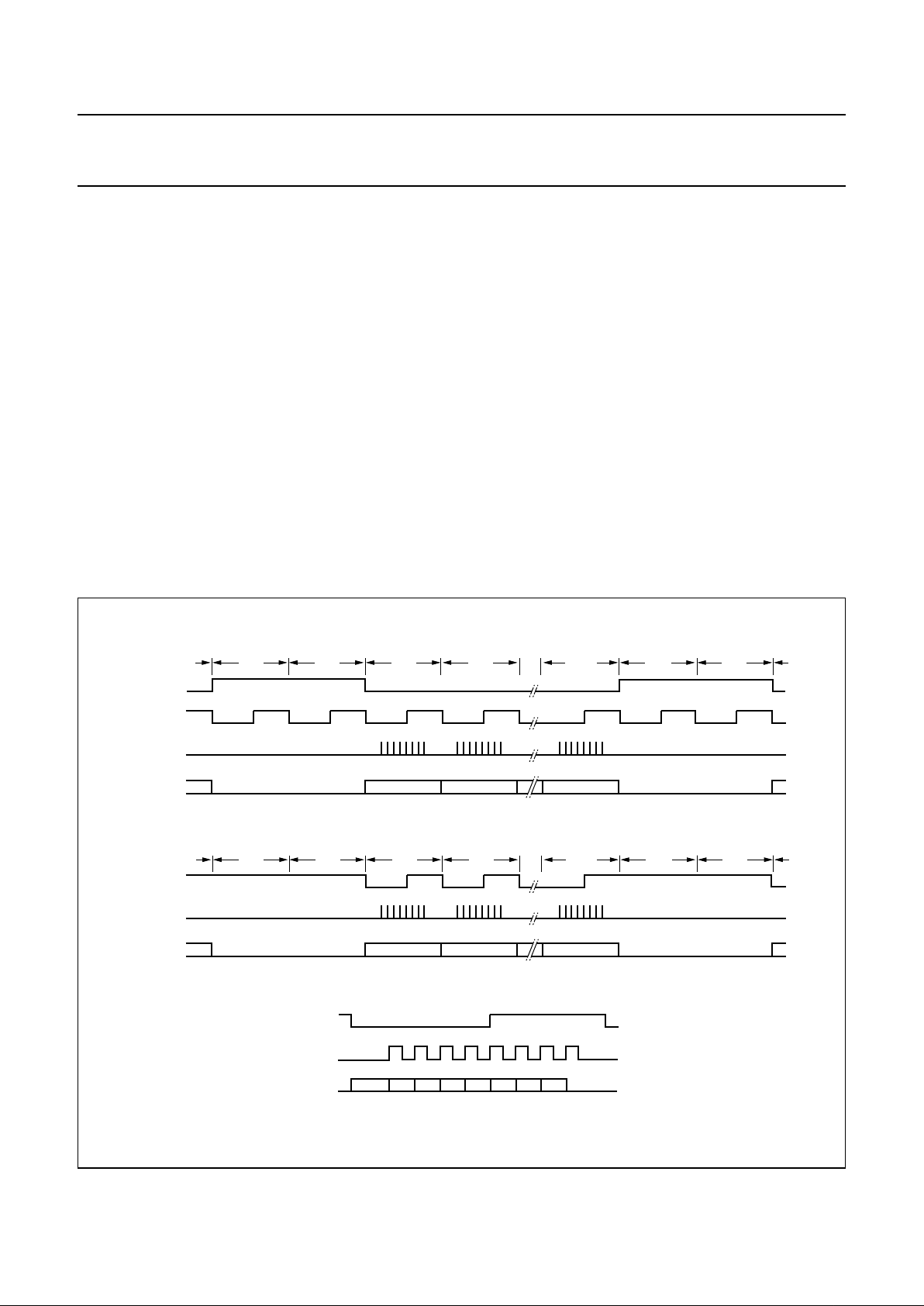
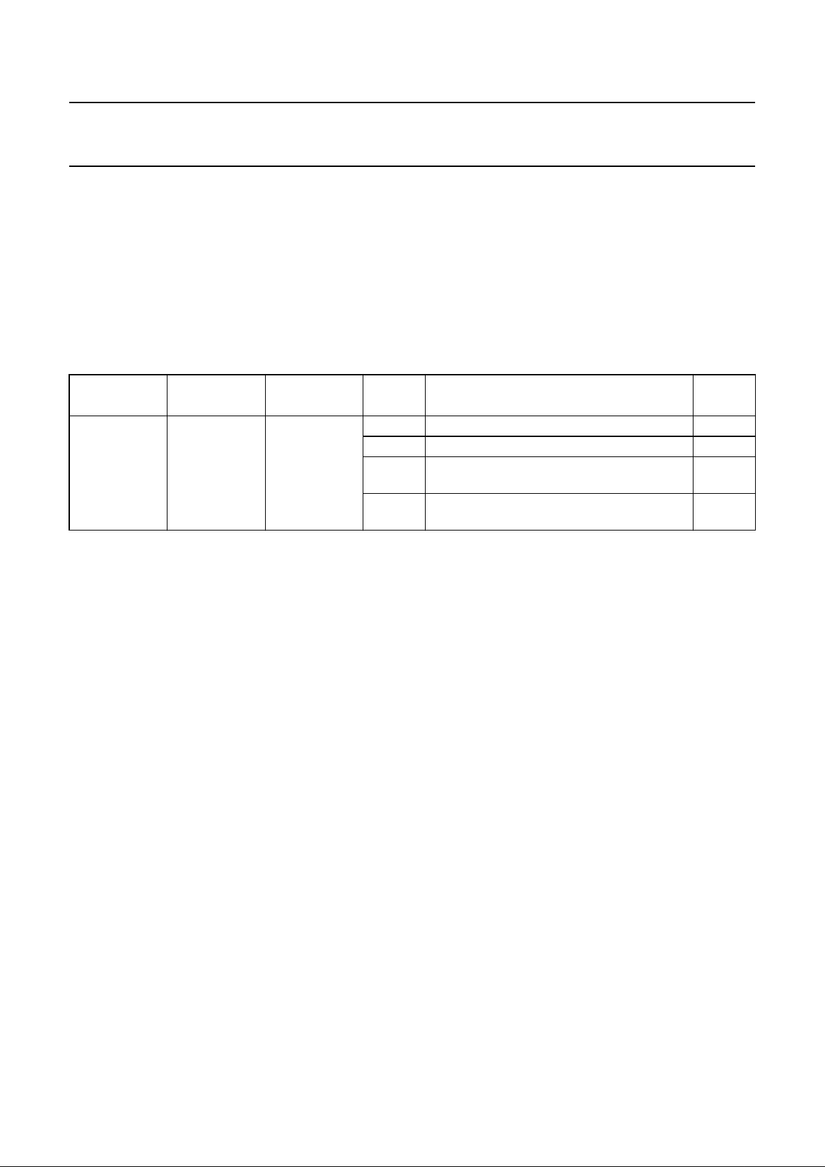
Data from all the subcode channels (P-to-W) may be read
via the subcode interface, which conforms to EIAJ
CP-2401. The interface is enabled and configured as
either a 3 or 4-wire interface via decoder register F.
The subcode interface output formats are illustrated in
Fig.8, where the RCK signal is supplied by another device
such as a CD graphics decoder.
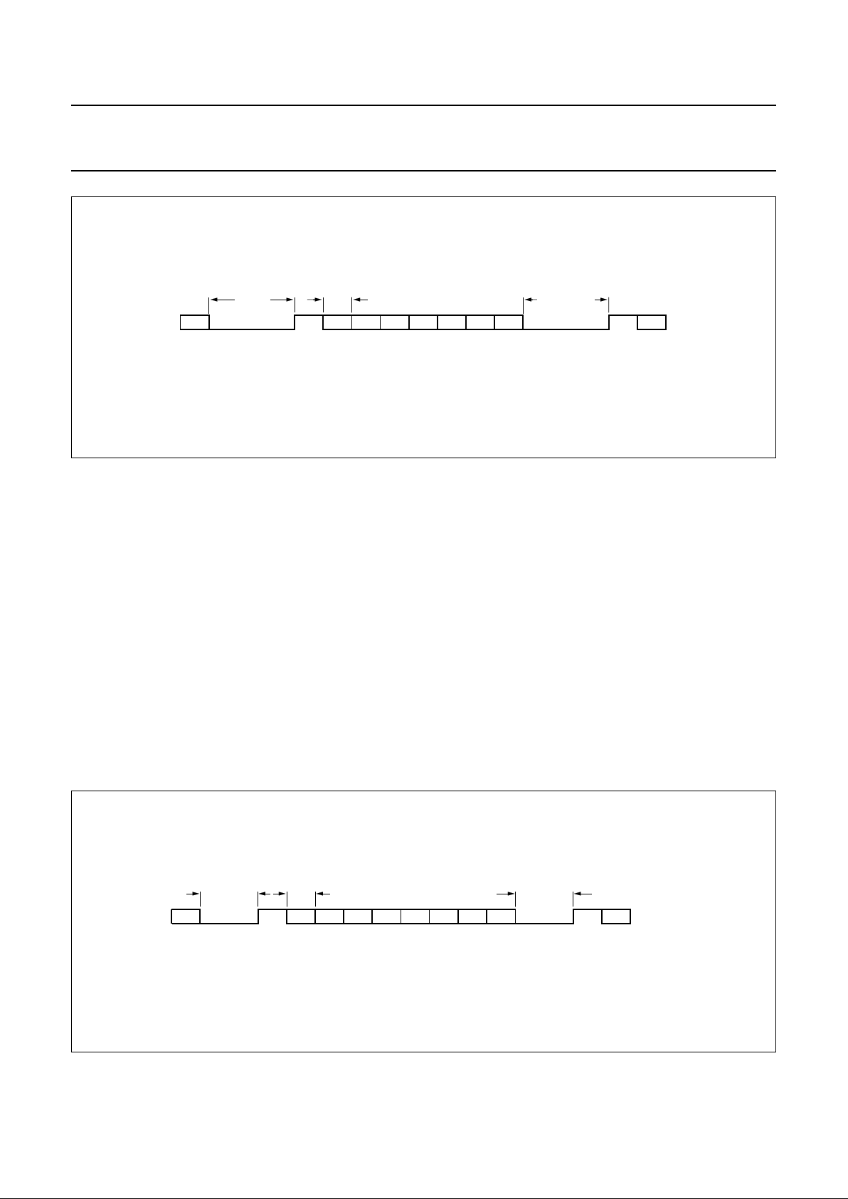
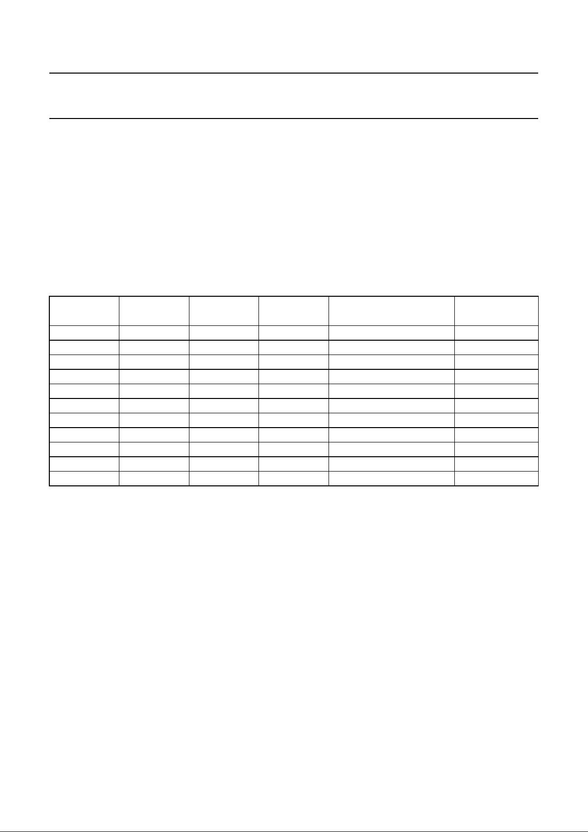
7.5.3 V4
SUBCODE INTERFACE
Data of subcode channels, Q-to-W, may be read via pin V4
if selected via decoder register D. The format is similar to
RS232 and is illustrated in Fig.9. The subcode sync word
is formed by a pause of 200 µs minimum. Each subcode
byte starts with a logic 1 followed by 7 bits (Q-to-W).
The gap between bytes is variable between
11.3 and 90 µs.
The subcode data is also available in the EBU output
(DOBM) in a similar format.
Fig.8 EIAJ subcode (CD graphics) interface format.
handbook, full pagewidth
SBSY
SFSY
RCK
SUB
SFSY
RCK
SUB
SFSY
RCK
SUB
EIAJ 4-wire subcode interface
EIAJ 3-wire subcode interface
SF0 SF1
SF2 SF3 SF97 SF0 SF1
P-W P-W P-W
P-W P-W P-W
PQRSTUVW
MBG410
SF0 SF1 SF2 SF3 SF97 SF0 SF1
1999 Jun 17 14
Philips Semiconductors Product specification
Digital servo processor and Compact Disc
decoder with integrated DAC (CD10)
SAA7325
Fig.9 Subcode format and timing on pin V4.
n = disc speed.
W96 1QRSTUVW 1Q
200 µs
min
11.3
µs
11.3 µs min
90 µs max
MGL719
7.6 FIFO and error corrector
The SAA7325 has a ±8 frame FIFO. The error corrector is
a t = 2, e = 4 type, with error corrections on both C1
(32 symbol) and C2 (28 symbol) frames. Four symbols are
used from each frame as parity symbols. This error
corrector can correct up to two errors on the C1 level and
up to four errors on the C2 level.
The error corrector also contains a flag processor. Flags
are assigned to symbols when the error corrector cannot
ascertain if the symbols are definitely good. C1 generates
output flags which are read after (de-interleaving) by C2,
to help in the generation of C2 output flags.
The C2 output flags are used by the interpolator for
concealment of uncorrectable errors. They are also output
via the EBU signal (DOBM). The EF output will flag bytes
in error in both audio and CD-ROM modes.
7.6.1 FLAGS OUTPUT (CFLG)
The flags output pin CFLG shows the status of the error
corrector and interpolator and is updated every frame
(7.35 × n kHz). In the SAA7325 chip a 1-bit flag is present
on the CFLG pin as illustrated in Fig.10. This signal shows
the status of the error corrector and interpolator.
The first flag bit, F1, is the absolute time sync signal, the
FIFO-passed subcode sync and relates the position of the
subcode sync to the audio data (DAC output). This flag
may also be used in a super FIFO or in the synchronization
of different players. The output flags can be made
available at bit 4 of the EBU data format (LSB of the 24-bit
data word), if selected by decoder register A.
Fig.10 Flag output timing diagram.
n = disc speed.
handbook, full pagewidth
F1 F2 F3 F4 F5 F6 F7 F8 F1F8
11.3
µs
33.9 µs
33.9 µs
MGL720
1999 Jun 17 15
Philips Semiconductors Product specification
Digital servo processor and Compact Disc
decoder with integrated DAC (CD10)
SAA7325
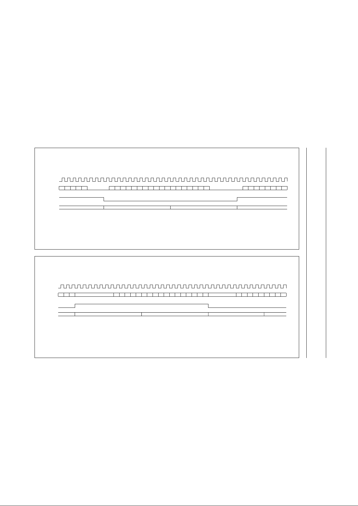
Table 2 Output flags
F1 F2 F3 F4 F5 F6 F7 F8 DESCRIPTION
0XXXXXXXno absolute time sync
1XXXXXXXabsolute time sync
X00XXXXXC1 frame contained no errors
X01XXXXXC1 frame contained 1 error
X10XXXXXC1 frame contained 2 errors
X11XXXXXC1 frame uncorrectable
X X X 0 0 X X 0 C2 frame contained no errors
X X X 0 0 X X 1 C2 frame contained 1 error
X X X 0 1 X X 0 C2 frame contained 2 errors
X X X 0 1 X X 1 C2 frame contained 3 errors
X X X 1 0 X X 0 C2 frame contained 4 errors
X X X 1 1 X X 1 C2 frame uncorrectable
XXXXX00Xno interpolations
XXXXX01Xat least one 1-sample interpolation
XXXXX10Xat least one hold and no interpolations
XXXXX11Xat least one hold and one 1-sample interpolation
7.7 Audio functions
7.7.1 D
E-EMPHASIS AND PHASE LINEARITY
When pre-emphasis is detected in the Q-channel
subcode, the digital filter automatically includes a
de-emphasis filter section. When de-emphasis is not
required, a phase compensation filter section controls the
phase of the digital oversampling filter to ≤±1° within the
band 0 to 16 kHz. With de-emphasis the filter is not phase
linear.
If the de-emphasis signal is set to be available at V5,
selected via decoder register D, then the de-emphasis
filter is bypassed.
7.7.2 D
IGITAL OVERSAMPLING FILTER
For optimizing performance with an external DAC, the
SAA7325 contains a 2 to 4 times oversampling IIR filter.
The filter specification of the 4 times oversampling filter is
given in Table 3.
These attenuations do not include the sample-and-hold at
the external DAC output or the DAC post filter. When using
the oversampling filter, the output level is scaled −0.5 dB
down to avoid overflow on full-scale sine wave inputs
(0 to 20 kHz).
Table 3 Filter specification
7.7.3 CONCEALMENT
A 1-sample linear interpolator becomes active if a single
sample is flagged as erroneous but cannot be corrected.
The erroneous sample is replaced by a level midway
between the preceding and following samples. Left and
right channels have independent interpolators. If more
than one consecutive non-correctable sample is found, the
last good sample is held. A 1-sample linear interpolation is
then performed before the next good sample (see Fig.11).
In CD-ROM modes (i.e. the external DAC interface is
selected to be in a CD-ROM format) concealment is not
executed.
PASS BAND STOP BAND ATTENUATION
0 to 9 kHz −≤0.001 dB
19 to 20 kHz −≤0.03 dB
− 24 kHz ≥25 dB
− 24 to 27 kHz ≥38 dB
− 27 to 35 kHz ≥40 dB
− 35 to 64 kHz ≥50 dB
− 64 to 68 kHz ≥31 dB
− 68 kHz ≥35 dB
− 69 to 88 kHz ≥40 dB
1999 Jun 17 16
Philips Semiconductors Product specification
Digital servo processor and Compact Disc
decoder with integrated DAC (CD10)
SAA7325
7.7.4 MUTE, FULL-SCALE, ATTENUATION AND FADE
A digital level controller is present on the SAA7325 which
performs the functions of soft mute, full-scale, attenuation
and fade; these are selected via decoder register 0:
• Mute: signal reduced to 0 in a maximum of 128 steps;
3ms
• Attenuate: signal scaled by −12 dB
• Full-scale: ramp signal back to 0 dB level; from mute
takes 3 ms
• Fade: activates a 128 stage counter which allows the
signal to be scaled up/down by 0.07 dB steps
– 128 = full-scale
– 120 = −0.5 dB (i.e. full-scale if oversampling filter
used)
–32=−12 dB
– 0 = mute.
7.7.5 PEAK DETECTOR
The peak detector measures the highest audio level
(absolute value) on positive peaks for left and right
channels. The 8 most significant bits are output in the
Q-channel data in place of the CRC bits. Bits 81 to 88
contain the left peak value (bit 88 = MSB) and
bits 89 to 96 contain the right peak value (bit 96 = MSB).
The values are reset after reading Q-channel data via
SDA.
Fig.11 Concealment mechanism.
Interpolation Hold Interpolation
MGA372
OK Error OK Error Error Error OK OK
1999 Jun 17 17
Philips Semiconductors Product specification
Digital servo processor and Compact Disc
decoder with integrated DAC (CD10)
SAA7325
7.8 DAC interface
7.8.1 I
NTERNAL BITSTREAM DIGITAL-TO-ANALOG CONVERTER (DAC)
The onboard bitstream DAC operates at a clock frequency of 96fs and is designed for operation with an audio input at
1fs. Optimum performance is dependent on the application circuit used and careful consideration should be given to the
recommended application circuits shown in Figs. 38 and 39. The onboard DAC is controlled from shadow register 7
(see Section 7.15.3 for definition of shadow registers). This shadow register controls routing of data into the onboard
DAC and also controls the DAC output pins, which can be held at zero when the onboard DAC is not required;
see Table 4.
Table 4 Shadow register
Audio data from the decoder part of SAA7325 can be routed as described in the following two subsections:
SHADEN
SHADOW
ADDRESS
REGISTER DATA FUNCTION RESET
1 0111 (7H) control of
onboard DAC
XXX0 hold onboard DAC outputs at zero reset
XXX1 enable onboard DAC outputs −
XX0X use external DAC or route audio data into
onboard DAC (loopback mode)
reset
XX1X route audio data into onboard DAC
(non-loopback mode)
−
7.8.1.1 Use onboard DAC
In this mode, shadow register 7 should be set to XX11.
This routes audio data from the decoder part of CD10 into
the onboard DAC and enables the DAC output pins
(LN, LP, RN and RP). It should be noted that the DAC
interface format (set by decoder register 3) must be set to
16-bit 1fs mode, either I2S-bus or EIAJ format, for optimum
DAC performance to be achieved. CD-ROM mode can
also be used if interpolation is not required.
When using this mode, the serial data output pins for
interfacing with an external DAC (SCLK, WCLK, DATA
and EF) are set to high-impedance.
7.8.1.2 Loopback external data into onboard DAC
The onboard DAC can also be set to accept serial data
inputs from an external source, e.g. an Electronic Shock
Absorption (ESA) IC. This is known as loopback mode and
is enabled by setting shadow register 7 to XX01. This
enables the serial data output pins (SCLK, WCLK, DATA
and EF) so that data can be routed from the SAA7325 to
an external ESA system (or external DAC).
The serial data from an external ESA IC can then also be
input to the onboard DAC on the SAA7325 by utilising the
serial data input interface (SCLI, SDI and WCLI).
In this mode, a wide range of data formats to the external
ESA IC can be programmed as shown in Table 5.
However, the serial input on the SAA7325 will always
expect the input data from the ESA IC to be 16 bit 1f
s
and
the same data format, either I2S-bus or EIAJ, as the serial
output format (set by decoder register 3).
1999 Jun 17 18
Philips Semiconductors Product specification
Digital servo processor and Compact Disc
decoder with integrated DAC (CD10)
SAA7325
7.8.2 EXTERNAL DAC INTERFACE
Audio data from the SAA7325 decoder can be sent to an
external DAC, identical to the SAA737x series. This is
similar to the ‘loopback’ mode, but in this case the internal
DAC outputs can be held at zero. i.e. shadow register 7 is
set to XX00. The SAA7325 is compatible with a wide range
of external DACs. Eleven formats are supported and are
given in Table 5. Figures 12 and 13 show the Philips
I2S-bus and the EIAJ data formats respectively. When the
decoder is operated in lock-to-disc mode, the SCLK
frequency is dependent on the disc speed factor ‘d’.
All formats are MSB first and f
s
is (44.1 × n) kHz.
The polarity of the WCLK and the data can be inverted;
selectable by decoder register 7. It should be noted that
EF is only a defined output in CD-ROM and 1fs modes.
When using an external DAC (or when using the onboard
DAC in non-loopback mode), the serial data inputs to the
onboard DAC (SCLI, SDI and WCLI) should be left
unconnected.
Table 5 DAC interface formats
Note
1. In this mode the first 16 bits contain data, but if any of the fade, attenuate or de-emphasis filter functions are activated
then the first 18 bits contain data.
REGISTER 3
SAMPLE
FREQUENCY
NUMBER OF
BITS
SCLK (MHz) FORMAT INTERPOLATION
1010 f
s
16 2.1168 CD-ROM (I2S-bus) no
1011 f
s
16 2.1168 CD-ROM (EIAJ) no
1110 f
s
16/18
(1)
2.1168 Philips I2S-bus 16/18 bits
(1)
yes
0010 f
s
16 2.1168 EIAJ 16 bits yes
0110 f
s
18 2.1168 EIAJ 18 bits yes
0000 4f
s
16 8.4672 EIAJ 16 bits yes
0100 4f
s
18 8.4672 EIAJ 18 bits yes
1100 4f
s
18 8.4672 Philips I2S-bus 18 bits yes
0011 2f
s
16 4.2336 EIAJ 16 bits yes
0111 2f
s
18 4.2336 EIAJ 18 bits yes
1111 2f
s
18 4.2336 Philips I2S-bus 18 bits yes
1999 Jun 17 19
Philips Semiconductors Product specification
Digital servo processor and Compact Disc
decoder with integrated DAC (CD10)
SAA7325
This text is here in white to force landscape pages to be rotated correctly when browsing through the pdf in the Acrobat reader.This text is here in
_white to force landscape pages to be rotated correctly when browsing through the pdf in the Acrobat reader.This text is here inThis text is here in
white to force landscape pages to be rotated correctly when browsing through the pdf in the Acrobat reader. white to force landscape pages to be ...
LEFT CHANNEL DATA (WCLK NORMAL POLARITY)
SCLK
15 14
15 1410DATA
WCLK
LSB error flag MSB error flag LSB error flag MSB error flag
EF
(CD-ROM
AND Ifs MODES ONLY)
01
MBG424
Fig.12 Philips I2S-bus data format (16-bit word length shown).
SCLK
17
170DATA
WCLK
0
LEFT CHANNEL DATA
MSB error flag LSB error flag MSB error flag
MBG423
EF
(CD-ROM
AND Ifs MODES ONLY)
Fig.13 EIAJ data format (18-bit word length shown).
1999 Jun 17 20
Philips Semiconductors Product specification
Digital servo processor and Compact Disc
decoder with integrated DAC (CD10)
SAA7325
7.9 EBU interface
The bi-phase mark digital output signal at pin DOBM is in
accordance with the format defined by the IEC958
specification. Three different modes can be selected via
decoder register A:
• DOBM pin held LOW
• Data taken before concealment, mute and fade (must
always be used for CD-ROM modes)
• Data taken after concealment, mute and fade.
7.9.1 FORMAT
The digital audio output consists of 32-bit words
(‘subframes’) transmitted in bi-phase mark code (two
transitions for a logic 1 and one transition for a logic 0).
Words are transmitted in blocks of 384. The formats are
given in Table 6.
Table 6 Format
Table 7 Description of table 6
Table 8 Bit assignment
FUNCTION BITS DESCRIPTION
Sync 0 to 3 −
Auxiliary 4 to 7 not used; normally zero
Error flags 4 CFLG error and interpolation flags when selected by register A
Audio sample 8 to 27 first 4 bits not used (always zero) twos complement LSB = bit 12, MSB = bit 27
Validity flag 28 valid = logic 0
User data 29 used for subcode data (Q-to-W)
Channel status 30 control bits and category code
Parity bit 31 even parity for bits 4 to 30
FUNCTION DESCRIPTION
Sync The sync word is formed by violation of the bi-phase rule and therefore does not contain any data.
Its length is equivalent to 4 data bits. The 3 different sync patterns indicate the following situations:
sync B: start of a block (384 words), word contains left sample; sync M: word contains left sample
(no block start) and sync W: word contains right sample.
Audio sample Left and right samples are transmitted alternately.
Validity flag Audio samples are flagged (bit 28 = 1) if an error has been detected but was uncorrectable.
This flag remains the same even if data is taken after concealment.
User data Subcode bits Q-to-W from the subcode section are transmitted via the user data bit. This data is
asynchronous with the block rate.
Channel status The channel status bit is the same for left and right words. Therefore a block of 384 words contains
192 channel status bits. The category code is always CD. The bit assignment is given in Table 8.
FUNCTION BITS DESCRIPTION
Control 0 to 3 copy of CRC checked Q-channel control bits 0 to 3; bit 2 is logic 1 when
copy permitted; bit 3 is logic 1 when recording has pre-emphasis
Reserved mode 4 to 7 always zero
Category code 8 to 15 CD: bit 8 = logic 1, all other bits = logic 0
Clock accuracy 28 to 29 set by register A; 10 = level I; 00 = level II; 01 = level III
Remaining 6 to 27 and 30 to 191 always zero
1999 Jun 17 21
Philips Semiconductors Product specification
Digital servo processor and Compact Disc
decoder with integrated DAC (CD10)
SAA7325
7.10 KILL circuit
The KILL circuit detects digital silence by testing for an
all-zero or all-ones data word in the left or right channel
prior to the digital filter. The output is switched to active
LOW when silence has been detected for at least 270 ms,
or if mute is active, or in CD-ROM modes. Two modes are
available which can be selected by decoder register C:
• Pin KILL: KILL active LOW indicates silence detected on
both left and right channels
• Pin KILL: KILL active LOW indicates silence detected on
left channel. V3 active LOW indicates silence detected
on right channel.
It should be noted that when mute is active or in CD-ROM
modes the output(s) are switched LOW.
7.11 Audio features off
The audio features can be turned off (selected by decoder
register E) which affects the following functions:
• Digital filter, fade, peak detector, KILL circuit (but
outputs KILL, V3 still active) are disabled
• V5 (if selected to be the de-emphasis flag output) and
the EBU outputs become undefined.
It should be noted that the EBU output should be set LOW
prior to switching the audio features off and after switching
audio features back on a full-scale command should be
given.
7.12 The VIA interface
The SAA7325 has four pins that can be reconfigured for
different applications. One of these pins, V2/V3, can be
programmed as an input (V2) or as an output (V3). Control
of the V2/V3 pin is via shadow register 3; see Table 9:
Selection of the V2/V3 pin does not affect the function
programmed by decoder register C i.e. the V2/V3 pin can
be changed from V2 to V3 function either before or after
setting the desired function via decoder register 1100.
Selection of, for instance, a V3 function while the V2/V3
pin is set to V2 will not affect the V2 functionality.
The functions of these versatile pins is identical to the
SAA737x series. The functions of these versatile pins is
programmed by decoder registers C and D, as shown in
Table 10.
Table 9 V2/V3 configuration
Table 10 Pin applications
SHADEN ADDRESS REGISTER DATA FUNCTION RESET
1 0011 (3H) control of
V2/V3 pin
0XXX V2/V3 pin configured as V2 input reset
1XXX V2/V3 pin configured as V3 output (open-drain) −
PIN NAME
PIN
NUMBER
TYPE
REGISTER
ADDRESS
REGISTER
DATA
FUNCTION
V1 63 input 1100 XXX1 external off-track signal input
− XXX0 internal off-track signal used; input may be read
via decoder status bit; selected via register 2
V2 36 input −−input may be read via decoder status bit;
selected via register 2
V3 36 output 1100 XX0X KILL output for right channel
− X01X output = 0
− X11X output = 1
V4 61 output 1101 0000 4-line motor drive (using V4 and V5)
− XX01 Q-to-W subcode output
− XX10 output = 0
− XX11 output = 1
V5 62 output 1101 01XX de-emphasis output (active HIGH)
− 10XX output = 0
− 11XX output = 1
 Loading...