

Philips saa7274 DATASHEETS

INTEGRATED CIRCUITS
DATA SH EET
SAA7274
Audio Digital Input Circuit (ADIC)
Product specification
File under Integrated Circuits, IC01
July 1991

Philips Semiconductors Product specification
Audio Digital Input Circuit (ADIC) SAA7274
GENERAL DESCRIPTION
The SAA7274 is an Audio Digital Input Circuit (ADIC) which converts digital audio signals in accordance with the
IEC/EBU standards, IEC tech. com. No. 84, secr. 50, Jan. 1987 into an equivalent binary value of data and control bits.
The output function of this device is to convert the equivalent binary value of data bits (for each channel) into a serial
digital audio signal which conforms to the I2S format.
Features
2
• I
S bus output
• Biphase audio signal (Satellite radio, compact disc and DAT)
QUICK REFERENCE DATA
PARAMETER CONDITIONS SYMBOL MIN. TYP. MAX. UNIT
Supply
Supply voltage range V
Inputs
except IBIFA
Input voltage HIGH V
Input voltage LOW V
Input current V
= 0 V −I
I
= 5.5 V I
V
I
Input capacitance C
Outputs
Output voltage HIGH V
Output voltage LOW V
Operating ambient
temperature range T
DD
IH
IL
I
I
I
OH
OL
amb
4.5 − 5.5 V
0.7 V
DD
0 − 0.3 V
− V
DD
DD
V
V
−−1µA
−−1µA
− 46 pF
VDD−0.5 −− V
−−0.4 V
−40 − +70 °C
PACKAGE OUTLINES
SAA7274P: 24-lead DIL; plastic (SOT101A); SOT101-1; 1996 September 05.
SAA7274T: 24-lead mini-pack; plastic (SO24; SOT137A); SOT137-1; 1996 September 05.
July 1991 2
Philips Semiconductors Product specification
Audio Digital Input Circuit (ADIC) SAA7274
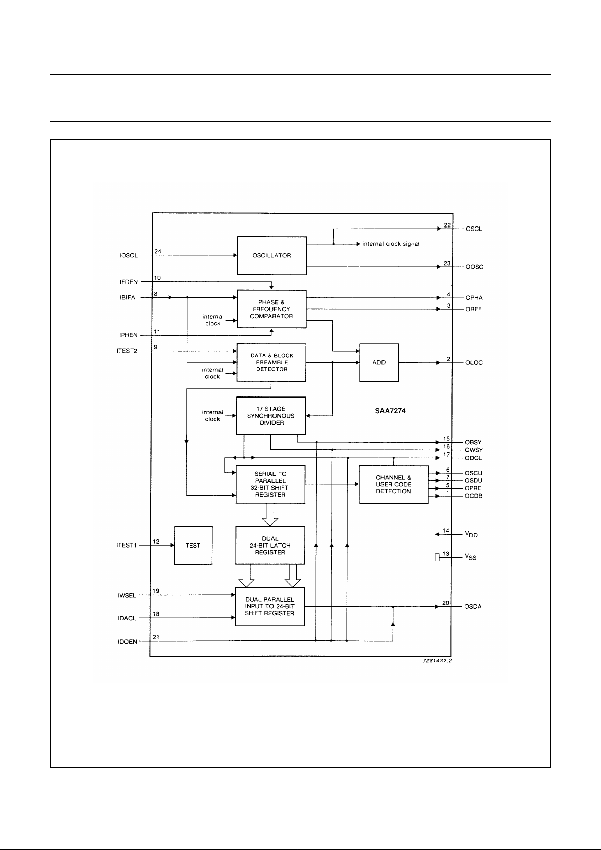
Fig.1 Block diagram.
July 1991 3
Philips Semiconductors Product specification
Audio Digital Input Circuit (ADIC) SAA7274
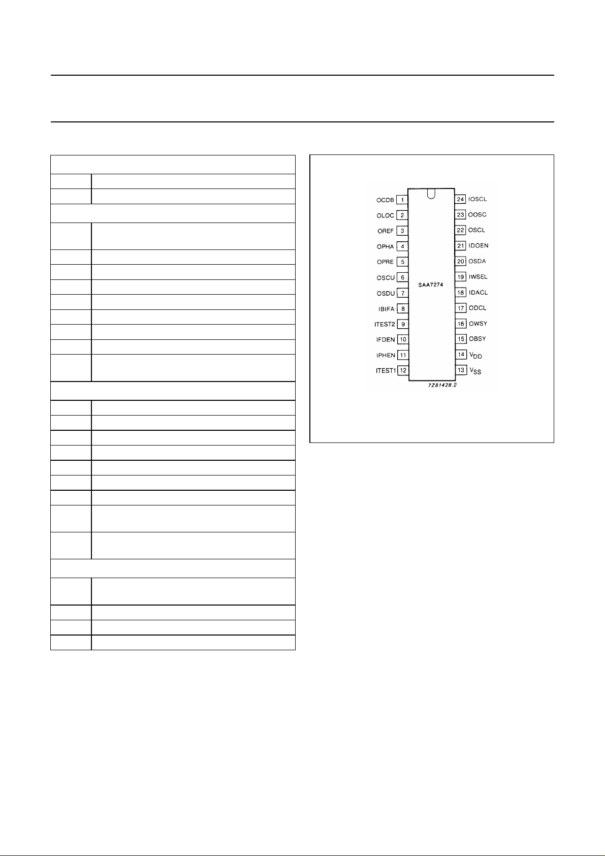
PINNING
Power supply
V
DD
V
SS
Inputs (CMOS protection)
IBIFA biphase input signal (min. 1 MHz;
IFDEN frequency detector enable
IPHEN phase-locked loop edge selector
ITEST1 test input enable
ITEST2 test input enable
IDACL data clock input signal (max. 5 MHz)
IWSEL word select input signal (max. 50 kHz)
IDOEN output enable
IOSCL clock oscillator input (min. 8 MHz;
positive supply voltage (5 V)
ground (0 V)
max. 3.1 MHz)
max. 12.5 MHz)
Outputs (CMOS push-pull)
OCDB control data bits (max. 400 kHz)
OLOC out-of-lock signal
OREF phase reference signal (max. 6.2 MHz)
OPHA phase output signal (max. 6.2 MHz)
OPRE pre-emphasis level
OSCU user clock/copy-bit signal (max. 3.1 MHz)
OSDU user data/pre-emphasis (max. 3.1 MHz)
OSCL system clock output (min. 8 MHz;
max. 12.5 MHz)
OOSC clock oscillator output (min. 8 MHz;
max. 12.5 MHz)
Outputs (3-state push-pull)
OBSY block synchronization output signal
(1/49152 system clock)
OWSY word clock output signal (1/256 system clock)
ODCL data clock output signal (1/4 system clock)
OSDA data output signal (max. 2.5 MHz)
Fig.2 Pinning diagram.
July 1991 4

Philips Semiconductors Product specification
Audio Digital Input Circuit (ADIC) SAA7274
FUNCTIONAL DESCRIPTION
Main function
The biphase input signal must conform to the IEC/EBU standards, IEC tech. com. No. 84, secr. 50, Jan. 1987 format,
as well as satisfying the following conditions:
• number of channels: 2
• transmission code: biphase mark
• synchronization method: biphase violation
• number of data bits: 24, starting with the LSB
• number of control bits: 4
• preamble values:
Table 1 Preamble values
preceding cell 0 1
block preamble 11101000 00010111
The main function performs the following tasks:
• Provides the output function with the equivalent binary value of the data bits separately for each of the two channels.
These values are available until new information is received.
• Generates an out-of-lock output signal (OLOC) which is HIGH when the frequency of the biphase input signal is equal
to 1/4 of the system clock frequency and when the block preambles are detected in the biphase input signal.
• If the biphase input signal is not present after 32 clock pulses and also whenever the biphase input signal and IOSCL/4
drift away from each other by more than 32 clock pulses, then the output OSCU is forced HIGH and output OSDU,
OPRE, OLOC, OCDB and OSDA are forced LOW.
• Generates a data clock output signal (ODCL) with a frequency of 1/4 of the system clock. When a block preamble is
detected in the biphase input signal ODCL is synchronized to a LOW value.
• Generates a word clock output signal (OWSY) with a frequency of 1/256 of the system clock. When a block preamble
is detected in the biphase input signal OWSY is synchronized to a LOW value.
• Generates a block synchronization output signal (OBSY). This signal is HIGH during 4 system clock periods and has
a frequency of 1/49152 of the system clock. The signal is synchronized with the block preambles of the biphase input
signal.
• Generates a phase output signal (OPHA) and a phase reference signal (OREF). If the frequency of the biphase input
signal (IBIFA) equals 1/4 of the system clock frequency (f
in Fig.3.
If the frequency of the biphase input signal (IBIFA) is greater or less than 1/4 of the system clock frequency then the
IC generates OPHA and OREF as shown in Fig.4.
/4) then the IC generates OPHA and OREF as shown
IOSCL
July 1991 5
 Loading...