

Philips saa7215, saa7216, saa7221 DATASHEETS

INTEGRATED CIRCUITS
DATA SH EET
SAA7215; SAA7216; SAA7221
Integrated MPEG AVGD decoders
Preliminary specification
Supersedes data of 1998 Sep 11
File under Integrated Circuits, IC02
2000 Jan 31

Philips Semiconductors Preliminary specification
Integrated MPEG AVGD decoders SAA7215; SAA7216; SAA7221
FEATURES
General features
• Integrated MPEG AVGD decoder: audio, video and
graphics decoding and digital video encoding
• 5 planes display chain:background colour, background
plane, MPEG display plane, graphics plane and cursor
plane
• 16-Mbit or 32-Mbit external Synchronous DRAM
(SDRAM) for MPEG audio and video decoding and
graphics data storage
• Single or double external SDRAM organized as
1M×16 or 2 × 1M×16 (two independent 16-bit data
bus) interfacing at 81 MHz. Due to efficient memory use
in MPEG decoding, more than 1 Mbit is available for
graphics in the single SDRAM configuration whereas
17 Mbits are available in the double SDRAM
configuration.
• All basic operations of the AVGD decoder are possible
in both 16- and 32-Mbit configuration; enhanced
performance is achieved by the use of 32-Mbit external
SDRAM
• Targeted to BSkyB 3.0 and Canal+ basic box and web
box specifications
• Fast 16-bit data + 22-bit address synchronous or
asynchronous interface with external controller at up to
40.5 MHz
• Dedicated input for compressed audio and video in
Packetized Elementary Stream (PES) or Elementary
Stream (ES) in byte wide or bit serial format.
Accompanyingstrobesignalsdistinguishbetweenaudio
and video data. Transport stream error correction
available.
• Audio and/or video can also be input via the CPU
interface in PES or ES in 8 or 16-bit parallel format
• Single 27 or 40.5 MHz external clock for time base
reference and internal processing. Internal system time
base at 90 kHz can be synchronized via CPU port.
All required decoding and presentation clocks are
generated internally.
• Flexible memory allocation under control of the external
CPU enables optimized partitioning of memory for
different tasks
• Optimum compatibility with T-MIPS controller family
(SAA7214, SAA7219 and successors)
• Boundary scan testing implemented
• External SDRAM self test
• Supply voltage: 3.3 V; package: SQFP208.
CPU related features
• 16-bit data, 22-bit address, Chip Select, Data Strobe
and DaTa ACKnowledge external control protocol
• Fast 16-bit data plus 22-bit address synchronous
interface with the SAA7214, SAA7219 family at up to
40.5 MHz
• Asynchronous interface possible with external
microcontroller
• Support of fast DMA transfer
• Flexible bidirectional interface to external SDRAM
• High speed/low latency interface with second graphics
SDRAM
• Byte access to the full SDRAM in the upper 16-Mbit
address range
• Independent memory mapping of SDRAM and control
registers
• Two programmable independent interrupt lines
available
• Supports Motorola 68xxx interfaces as well as LSI
L64108 interface.
MPEG-2 system features
• Parsing of MPEG-2 PES and MPEG-1 packet streams
• Double system time clock counters
• Stand-alone or supervised audio/video synchronization
• Processing of errors flagged by channel decoding
section.
MPEG-2 video features
• Decodingof MPEG-2 video upto main level, main profile
• Output picture format: CCIR-601 4 : 2 : 2 interlaced
pictures.Pictureformat720 × 576at 50 Hz or 720 × 480
at 60 Hz.
• Support of constant and variable bit rates up to
15 Mbits/s for the elementary stream
• Horizontal and vertical pan and scan allows the
extraction of a window from the coded picture
• Flexible horizontal scaling from 0.5 up to 4 allows easy
aspect ratio conversion including support for 2.21 : 1
aspect ratio movies; in case of shrinking an anti-aliasing
pre-filter is applied
2000 Jan 31 2

Philips Semiconductors Preliminary specification
Integrated MPEG AVGD decoders SAA7215; SAA7216; SAA7221
• Vertical scaling with fixed factors 0.5, 0.75, 1 or 2;
factor 0.5 realizes picture shrink. Factor 2 can be used
for up-conversion of pictures with 288 (240) lines or
less; factor 0.75 is used for letterbox presentation.
• Horizontaland vertical scaling can be combinedtoscale
pictures to1⁄4of their original size, thus freeing up
screen space for graphic applications like electronic
program guides
• Non full screen MPEG pictures can be displayed in a
box of which position and background colour are
adjustable by the external microcontroller; structured
background is available as part of the graphic features
• Nominal video input buffer size for MP at ML 2.7-Mbit
• Video output may be slaved to internally (master)
generated or externally (slave) supplied
HV synchronization signals or CCIR-656 contained
synchronization signals. The position of active video is
programmable. Display phase is not affected by MPEG
timebase changes.
• Decoding and presentation can be independently
handled under CPU control
• Various trick modes under control of external
microcontroller:
– Freeze field/frame on I- or P-frames; restart on
I-picture
– Freeze field on B-frames; restart at any moment
– Scanning and decoding of I- or I- and P-frames in a
IBP sequence
– Single step mode
– Repeat/skip field for time base correction
– Repeat/skip frame for display parity integrity.
• Synchronization modes: DTS controlled, DTS free
running, software controlled, buffer controlled
• DTS register can be set via external controller;
programmable processing delay compensation.
MPEG-2 audio features
• Supported audio sampling frequencies:
48, 44.1, 32, 24, 22.05 and 16 kHz
• Independentchannelvolumecontrolandprogrammable
inter-channel crosstalk through a baseband audio
processing unit
• MPEG audio decoder
– Decoding of 2 channels, layer I and IIMPEG-1 audio
and low sampling frequency extension of MPEG-2
– Supports for mono, stereo, intensity stereo and dual
channel mode
– CRC error detection with automatic mute
– Constant and variable bit rates up to 448 kbit/s
– Selectable output channel in dual channel mode
– Storage of last 54 bytes in ancillary data field
– Dynamic range control at output.
• Muting possibility via external controller; automatic
muting in case of errors
• Generation of ‘beeps’ with programmable tone height,
duration and amplitude
• Linear PCM decoding
– Support for up to 8 channels linear PCM elementary
audio streams
– Supports for 8, 16, 20 and 24 bit/sample
– Supports for bit rates up to 6.144 Mbit/s
– 96 kHz LPCM samples will be mapped to a 48 kHz
multi-channel format
– Volume control for linear PCM samples in three
steps: −6, −12 and −18 dB.
• Burst-formatting for interconnection with an external
multi-channel decoder
– AC-3 elementary streams (IEC1937)
– MPEG-2 multi-channel streams in ES or PES format
– Output via the digital audio output or the IEC 958
output.
• Output stage
– Global control for volume and balance
– Serial multi-channel digital audio output with 16, 18,
20 or 22 bits per sample, compatible either to I2Sor
Japanese formats; output can be set to high
impedance mode via the external controller
– IEC958 (Serial SPDIF) audio output; output can be
set to high impedance mode
– Clock output 256 or 384 × fs for external
DA converter or clock input; output can be set to high
impedance mode.
• Audio FIFO in external SDRAM; programmable buffer
size, at least 64 kbit is available
• Synchronization modes: PTS controlled, PTS free
running, software controlled, buffer controlled
• PTS register can be set via external controller;
programmable processing delay compensation.
Background colour
• 24 bit YCbCr colour.
2000 Jan 31 3

Philips Semiconductors Preliminary specification
Integrated MPEG AVGD decoders SAA7215; SAA7216; SAA7221
Graphics features
2 nearly identical graphics planes: the first graphics plane
commonly called the background plane and the second
graphics plane commonly called foreground plane.
The following features apply for both planes.
• Graphics is presented in boxes independent of video
format
• Boxes can be up to full screen allowing double buffer
display mechanism
• Two independent data paths with RGB 4 :4:4 and
YCbCr 4 : 2 : 2 formats available with independent
mixing
• RGB path transparent to YCbCr format
• Conversion matrices available to allow any format on
any different data path (RGB or YCbCr)
• Screen arrangement of boxes is determined by display
list mechanism which allows for multiple boxes,
background loading, fast switching, scrolling,
overlapping and fading of regions
• Real-time anti-flickering performed in hardware;
programmable hardware available for off-line
anti-flickering
• Hard edged or soft edged wiping of regions available
• Support of 2, 4, 8, 16 bit/pixel infixed bit maps format or
coded in accordance to the DVB variable/run length
standard for region based graphics
• Chrominance down-sampling filter switched per region
• Display colours are obtained via colour look up tablesor
directly from bitmap; CLUT output can be YCbCrT at
8-bit for each signal component thus enabling 16 M
different colours and 6-bit for T which gives 64 mixing
levels with video; CLUT output can also be RGBT with
same resolutions; non linear processing available by
means of LUTs
• Map table mechanism to specify a sub set of entries if
the CLUT is larger than required by the coded bit
pattern; supported map tables are 16 to 256, 4 to 256
and4to16
• Up to 4 graphics boxes may overlap vertically even
inside one graphics layer thanks to the use of flexible
chained descriptors
• Graphics mechanism can be used for signal generation
in the vertical blanking interval; useful for teletext, wide
screen signalling, closed caption etc.
In addition to the previous listed features, the second
graphics plane sustains:
• Teletext insertion with automatic teletext data retrieving
from the external SDRAM.
Data manipulation unit
• Powerful 3D block move with different patterns for
source and destination area
• Dedicated events for video synchronization
• Scaling, format conversion and bit manipulation from a
chained list of instructions.
Cursor
• Size of 1024 pixels
• Programmable shape (8 × 128, 16 × 64, 32 × 32,
64 × 16 and 128 × 8)
• 16 colours available with a 4 level transparency mixing
with video and graphics
• Cursor colours obtained via two 16 entry CLUTs with
YCbCrTat6, 4, 4respectively 2 bits and RGBT at 4, 4, 4
respectively 4 bits (or 4, 5, 3, respectively 4 bits)
• Cursor can be moved freely across the screen without
overlapping restrictions.
Digital output
• Programmable selection for the mixed graphics planes
with video for the CVBS and RGB outputs
• Digital video input/output interface on 8 bit,
27 MHz (CbYCrY multiplexed bus), at a CCIR-656
format.
Analog output
• Analog video output interface on both the RGB and
Y/C/CVBS formats available simultaneously
• PAL/NTSC/SECAM encoding (SAA7221HS only)
• Two DACs for CVBS, Y and C, CVBS running at
27 MHz 10-bit resolution
• Three DACs for R (Y), G (Cb) and B (Cr) running at
27 MHz; 9-bit resolution connected to a 10-bit inputDAC
• Closed captioning and teletext encoding on CVBS
• Macrovision 7.01 and 6.1 encoding capability on
Y or CVBS and C or CVBS (SAA7216HS only).
2000 Jan 31 4
Philips Semiconductors Preliminary specification
Integrated MPEG AVGD decoders SAA7215; SAA7216; SAA7221
APPLICATIONS
The SAA7215 integrated MPEG AVGD decoder is aimed
at being used in MPEG digital TV applications. This
decoder is primarily designed to be connected to a
SAA7214 transport stream descrambler/demultiplexer/
microcontroller by means of glueless interfaces even
though connections to other market demultiplexers and/or
microcontrollers are possible. Compatibility is also
targeted with the SAA7219 and with the successor of the
T-MIPS family.
The SAA7215 can be used in any system where high-end
GENERAL DESCRIPTION
The SAA7215HS, SAA7216HS, SAA7221H is a MPEG-2
sourcedecoderwhichcombinesaudiodecodingandvideo
decoding. Additionally to these basic MPEG functions it
also provides means for enhanced graphics, background
display and/or on-screen display as well as encoding of
output video. Due to an optimized architecture for audio
and video decoding, maximum capacity in external
memory and processing power from the external CPU is
available for graphics support.
Possible options are indicated in Table 1.
graphics are needed (associated SDRAM can be
extended to 32-Mbit) as well as in low cost systems (all
functions can be enabled with only 16-Mbit of associated
SDRAM).
Table 1 Possible options
TYPE NUMBER MACROVISION SECAM
SAA7215HS/C2 no no
SAA7216HS/C1 yes no
SAA7221HS/C1 no yes
QUICK REFERENCE DATA
SYMBOL PARAMETER MIN. TYP. MAX. UNIT
V
DD
I
DD
functional supply voltage range 3.0 3.3 3.6 V
total supply current; VDD= 3.3 V − tbf − mA
CLK device clock input frequency (2 solutions are possible) −30 ppm +27 +30 ppm MHz
−30 ppm +40.5 +30 ppm MHz
ORDERING INFORMATION
PACKAGE
TYPE NUMBER
NAME DESCRIPTION VERSION
SAA7215HS/C2 SQFP208 plastic shrink quad flat package; 208 leads (lead length 1.3 mm);
SAA7216HS/C1
body 28 × 28 × 3.4 mm
SOT316-1
SAA7221HS/C1
2000 Jan 31 5
Philips Semiconductors Preliminary specification
Integrated MPEG AVGD decoders SAA7215; SAA7216; SAA7221
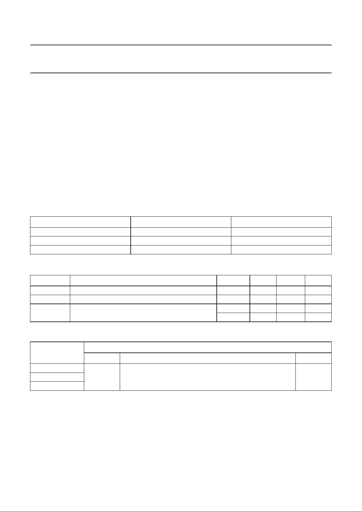
BLOCK DIAGRAMS
handbook, full pagewidth
MPEG
data
audio
DACs
16-Mbit SDRAM
(compulsory)
MEMORY INTERFACE 1 MEMORY INTERFACE 2
AUDIO/VIDEO
INTERFACE
SYSTEM TIME
BASE UNIT
VIDEO INPUT BUFFER
& SYNCHRONIZATION
VIDEO DECODER
AUDIO INPUT BUFFER
& SYNCHRONIZATION
AUDIO DECODER
data
data
16-Mbit SDRAM
(optional)
DATA MANIPULATION
DIGITAL ENCODER
DIGITAL VIDEO
SYNCHRONIZATION
CURSOR UNIT
GRAPHICS
UNIT 2
UNIT
analog
video
digital
video
CLK
CPU
CLOCK GENERATION
JTAG
HOST INTERFACE
Fig.1 Block diagram.
2000 Jan 31 6
control
GRAPHICS
UNIT 1
DISPLAY UNIT
FCE107
Philips Semiconductors Preliminary specification
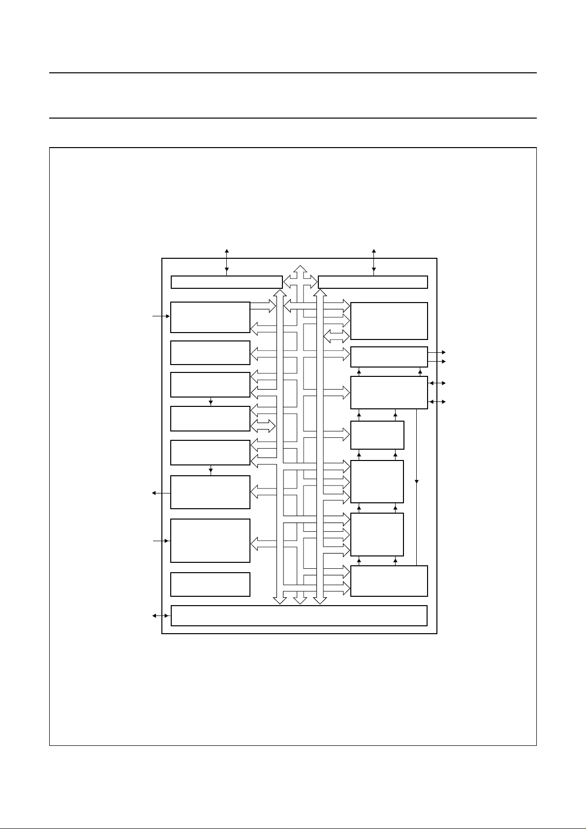
Integrated MPEG AVGD decoders SAA7215; SAA7216; SAA7221
handbook, full pagewidth
MPEG
data
audio
DACs
16-Mbit SDRAM
MEMORY INTERFACE 1 MEMORY INTERFACE 2
AUDIO/VIDEO
INTERFACE
SYSTEM TIME
BASE UNIT
VIDEO INPUT BUFFER
& SYNCHRONIZATION
VIDEO DECODER
AUDIO INPUT BUFFER
& SYNCHRONIZATION
AUDIO DECODER
data
DATA MANIPULATION
DIGITAL ENCODER
DIGITAL VIDEO
SYNCHRONIZATION
CURSOR UNIT
GRAPHICS
UNIT 2
UNIT
analog
video
digital
video
CLK
CPU
CLOCK GENERATION
JTAG
HOST INTERFACE
Fig.2 Block diagram with preferred use in 16-Mbit configuration.
2000 Jan 31 7
control
GRAPHICS
UNIT 1
DISPLAY UNIT
FCE108

Philips Semiconductors Preliminary specification
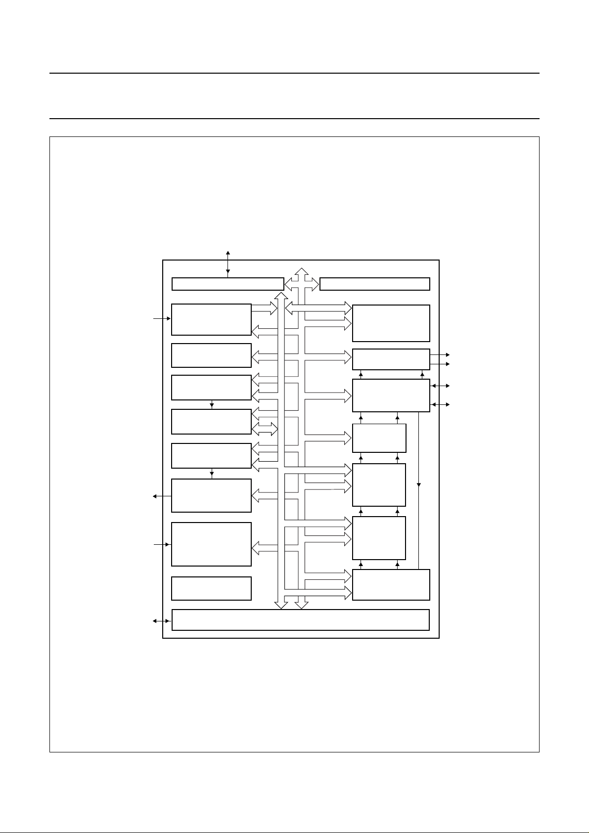
Integrated MPEG AVGD decoders SAA7215; SAA7216; SAA7221
handbook, full pagewidth
MPEG
data
audio
DACs
16-Mbit SDRAM
(MPEG)
MEMORY INTERFACE 1 MEMORY INTERFACE 2
AUDIO/VIDEO
INTERFACE
SYSTEM TIME
BASE UNIT
VIDEO INPUT BUFFER
& SYNCHRONIZATION
VIDEO DECODER
AUDIO INPUT BUFFER
& SYNCHRONIZATION
AUDIO DECODER
data
data
16-Mbit SDRAM
(Graphics)
DATA MANIPULATION
DIGITAL ENCODER
DIGITAL VIDEO
SYNCHRONIZATION
CURSOR UNIT
GRAPHICS
UNIT 2
UNIT
analog
video
digital
video
CLK
CPU
CLOCK GENERATION
JTAG
HOST INTERFACE
Fig.3 Block diagram with preferred use in 32-Mbit configuration.
2000 Jan 31 8
control
GRAPHICS
UNIT 1
DISPLAY UNIT
FCE109

Philips Semiconductors Preliminary specification
Integrated MPEG AVGD decoders SAA7215; SAA7216; SAA7221
PINNING
Pinning table (listed numerically)
SYMBOL PIN TYPE
V
SS
1 S ground for pad ring
(1)
DESCRIPTION
DATA(4) 2 I/O CPU data input or output (bit 4); note 2
DATA(5) 3 I/O CPU data input or output (bit 5); note 2
DATA(6 4 I/O CPU data input or output (bit 6); note 2
DATA(7) 5 I/O CPU data input or output (bit 7); note 2
DATA(8) 6 I/O CPU data input or output (bit 8); note 2
DATA(9) 7 I/O CPU data input or output (bit 9); note 2
V
DD
8 S supply voltage for pad ring
DATA(10) 9 I/O CPU data input or output (bit 10); note 2
DATA(11) 10 I/O CPU data input or output (bit 11); note 2
DATA(12) 11 I/O CPU data input or output (bit 12); note 2
DATA(13) 12 I/O CPU data input or output (bit 13); note 2
DATA(14) 13 I/O CPU data input or output (bit 14); note 2
DATA(15) 14 I/O CPU data input or output (bit 15); note 2
V
SS
15 S ground for pad ring
SDRAM_ADDR1(3) 16 O SDRAM address 1 output (bit 3)
SDRAM_ADDR1(2) 17 O SDRAM address 1 output (bit 2)
SDRAM_ADDR1(4) 18 O SDRAM address 1 output (bit 4)
SDRAM_ADDR1(1) 19 O SDRAM address 1 output (bit 1)
SDRAM_ADDR1(5) 20 O SDRAM address 1 output (bit 5)
SDRAM_ADDR1(0) 21 O SDRAM address 1 output (bit 0)
V
DD
22 S supply voltage for pad ring
SDRAM_ADDR1(6) 23 O SDRAM address 1 output (bit 6)
SDRAM_ADDR1(10) 24 O SDRAM address 1 output (bit 10)
SDRAM_ADDR1(7) 25 O SDRAM address 1 output (bit 7)
V
SS(CO)
V
DD(CO)
26 S ground for core logic
27 S supply voltage for digital core logic
SDRAM_ADDR1(11) 28 O SDRAM address 1 output (bit 11)
SDRAM_ADDR1(9) 29 O SDRAM address 1 output (bit 9)
SDRAM_ADDR1(8) 30 O SDRAM address 1 output (bit 8)
V
SS
31 S ground for pad ring
SDRAM_UDQ1 32 O SDRAM write mask 1 output
SDRAM_RAS1 33 O SDRAM row address strobe1 output
SDRAM_CAS1 34 O SDRAM column address 1 output
SDRAM_WE1 35 O SDRAM write enable 1 output
V
DD
36 S supply voltage for pad ring
SDRAM_DATA1(8) 37 I/O SDRAM data 1 input or output (bit 8)
SDRAM_DATA1(7) 38 I/O SDRAM data 1 input or output (bit 7)
2000 Jan 31 9
 Loading...