

Philips saa7207h DATASHEETS

INTEGRATED CIRCUITS
DATA SH EET
SAA7207H
Reed Solomon decoder IC
Product specification
File under Integrated Circuits, IC02
1996 Jul 17
Philips Semiconductors Product specification
Reed Solomon decoder IC SAA7207H
FEATURES
• (204, 188 and 17) Digital Video Broadcasting (DVB)
compliant Reed Solomon (RS) codes
• Automatic synchronization of bytes, blocks and frame
• Convolutional de-interleaving (I = 12)
• Energy dispersal de-randomizing
• Contained in a 44-pin quad flat package
• I2C-bus interface
• 6 quasi-bidirectional ports
• Boundary scan facility.
QUICK REFERENCE DATA
SYMBOL PARAMETER MIN. TYP. MAX. UNIT
V
DD
I
DD(tot)
T
CLK
operational supply voltage 4.75 5.00 5.25 V
total supply current − 65 − mA
input clock period − 31.5 − ns
APPLICATIONS
• Forward Error Correction (FEC) for digital TV
distribution according to the DVB standard.
ORDERING INFORMATION
PACKAGE
TYPE NUMBER
NAME DESCRIPTION VERSION
SAA7207H/C1 QFP44 plastic quad flat package; 44 leads (lead length 1.3 mm);
body 10 × 10 × 1.75 mm
SOT307-2
1996 Jul 17 2
Philips Semiconductors Product specification
Reed Solomon decoder IC SAA7207H
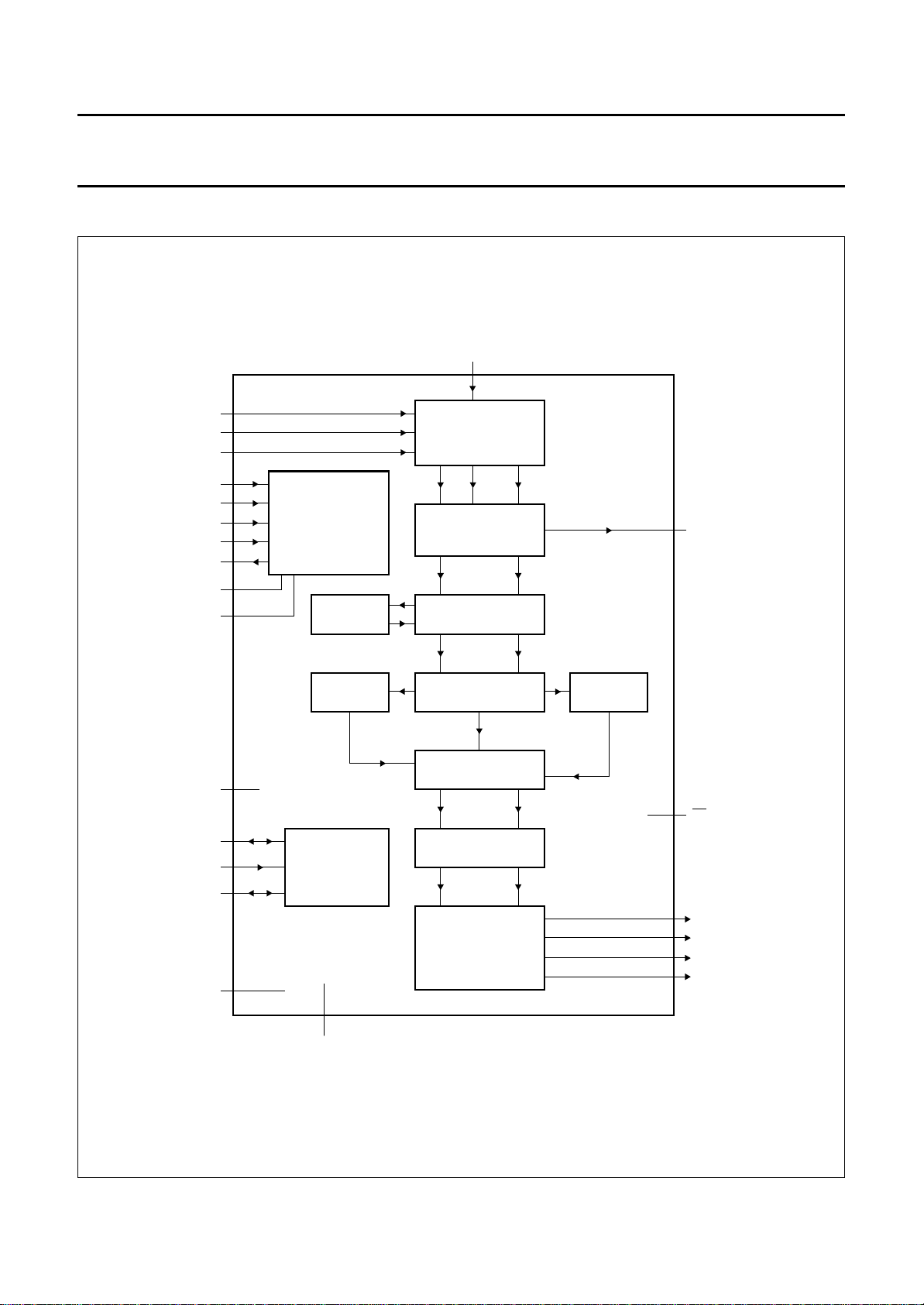
BLOCK DIAGRAM
handbook, full pagewidth
DATA1
DATA0
VALI
TRST
TCK
TMS
TDI
TDO
TC0
TC1
RESET
SDA
SCL
PORT5
to
PORT0
V
DD
35
36
34
3
4
5
6
7
41
42
43
44
1
27 to 32
10, 18, 25,
33, 39
TEST
CONTROL BLOCK
FOR
BOUNDARY
SCAN TEST
AND
SCAN TEST
RAM D
RAM M
2
C-BUS
I
INTERFACE
SAA7207H
8, 14, 22,
26, 37, 40
V
SS
CLK
38
INPUT
INTERFACE
1/2CLK VALI DATA (0 : 3)
SYNCHRONIZATION
1/4CLK DATA (7 : 0)
DE-INTERLEAVING
1/4CLK DATA (7 : 0)
SYNDROME
CALCULATION
syndrome
coefficient
ERROR
CORRECTION
1/4CLK DATA (7 : 0)
DESCRAMBLER
1/4CLK DATA (7 : 0)
OUTPUT
INTERFACE
RAM B
BUFFER
11, 12, 13, 15,
16,17,19, 20,
2
21
9
24
23
MBH315
NOSYNC
OE
BYTEO0
to
BYTEO7
BCLK
BEGIN
BERR
1996 Jul 17 3
Fig.1 Block diagram.

Philips Semiconductors Product specification
Reed Solomon decoder IC SAA7207H
PINNING
SYMBOL PIN I/O DESCRIPTION
2
SCL 1 I serial clock input (I
NOSYNC 2 O not synchronized output (1 = not synchronized)
TRST 3 I boundary scan test reset (0 = active)
TCK 4 I boundary scan test clock
TMS 5 I boundary scan test mode select (1 = BST select)
TDI 6 I boundary scan test data input
TDO 7 O boundary scan test data output
V
SS
BCLK 9 O*
V
DD
BYTEO0 11 O*
BYTEO1 12 O*
BYTEO2 13 O*
V
SS
BYTEO3 15 O*
BYTEO4 16 O*
BYTEO5 17 O*
V
DD
BYTEO6 19 O*
BYTEO7 20 O*
8 − ground
(1)
byte clock output
10 − positive supply voltage
(1)
(1)
(1)
output data byte 0 (LSB)
output data byte 1
output data byte 2
14 − ground
(1)
(1)
(1)
output data byte 3
output data byte 4
output data byte 5
18 − positive supply voltage
(1)
(1)
output data byte 6
output data byte 7 (MSB)
OE 21 I output enable not (active LOW; 1 = O*
V
SS
BERR 23 O*
BEGIN 24 O*
V
DD
V
SS
22 − ground
(1)
(1)
block error output (1 = uncorrectable block)
begin of block output (1st byte of block is output)
25 − positive supply voltage
26 − ground
PORT5 27 I/O quasi-bidirectional port 5
PORT4 28 I/O quasi-bidirectional port 4
PORT3 29 I/O quasi-bidirectional port 3
PORT2 30 I/O quasi-bidirectional port 2
PORT1 31 I/O quasi-bidirectional port 1
PORT0 32 I/O quasi-bidirectional port 0
V
DD
33 − positive supply voltage
VALI 34 I valid input (1 = data is valid)
DATA1 35 I input data 1 (MSB)
DATA0 36 I input data 0 (LSB)
V
SS
37 − ground
CLK 38 I master clock input (also acting as input data clock)
V
DD
V
SS
39 − positive supply voltage
40 − ground
C-bus)
(1)
high impedance)
1996 Jul 17 4
Philips Semiconductors Product specification
Reed Solomon decoder IC SAA7207H
SYMBOL PIN I/O DESCRIPTION
TC0 41 I test mode control input 0 (0 = application mode)
TC1 42 I test mode control input 1 (0 = application mode)
RESET 43 I master reset input (1 = active)
2
SDA 44 I/O bidirectional serial data port (I
Note
1. When OE is active (pin 21 = HIGH), all O* outputs become high impedance.
C-bus)
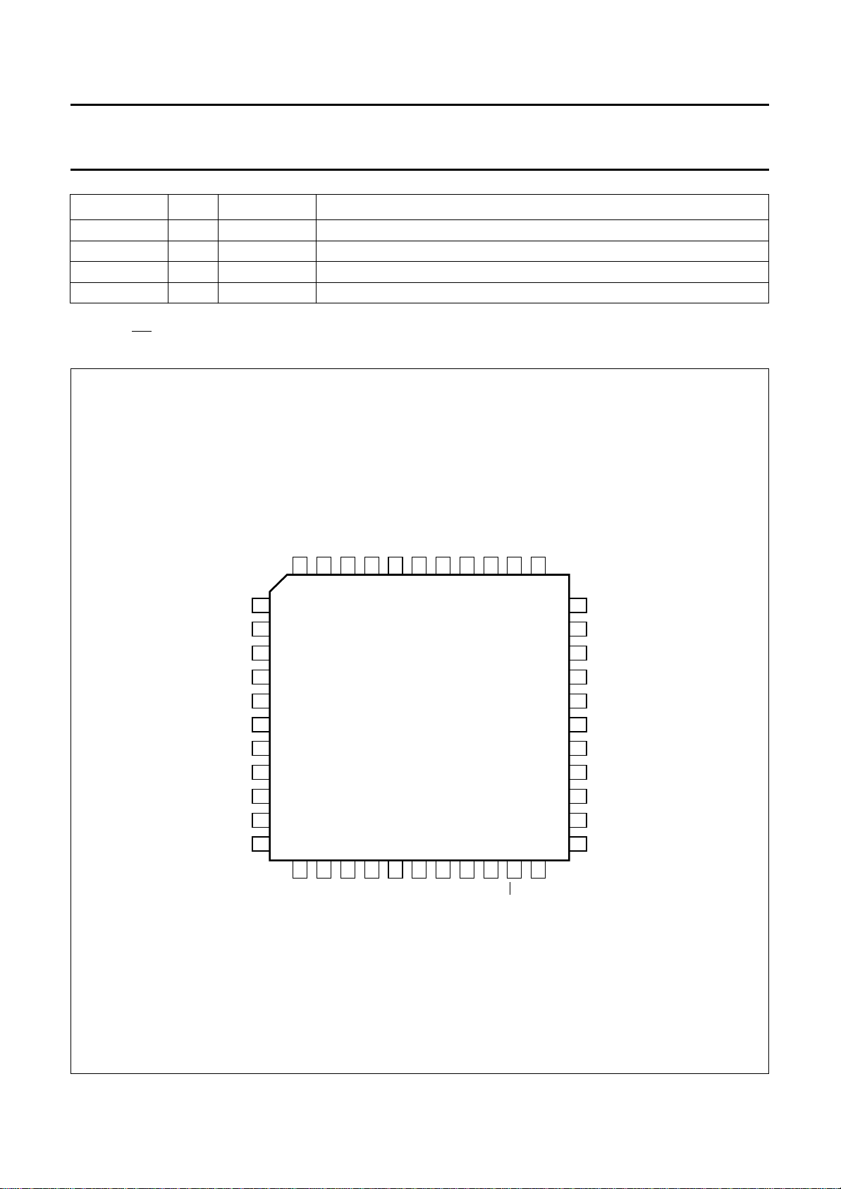
handbook, full pagewidth
SCL
NOSYNC
TRST
TCK
TMS
TDI
TDO
V
SS
BCLK
V
DD
BYTEO0
CLK
38
18
DD
V
SS
DATA0
V
37
36
19
20
BYTEO6
BYTEO7
DATA1
35
21
OE
VALI
34
22
SS
V
33
32
31
30
29
28
27
26
25
24
23
MBH314
V
DD
PORT0
PORT1
PORT2
PORT3
PORT4
PORT5
V
SS
V
DD
BEGIN
BERR
SDA
44
43
42
41
1
2
3
4
5
6
7
8
9
10
11
12
13
14
15
SS
V
BYTEO1
BYTEO2
BYTEO3
V
V
40
39
SAA7207H
16
17
BYTEO4
BYTEO5
DD
SS
TC0
TC1
RESET
1996 Jul 17 5
Fig.2 Pin configuration.
Philips Semiconductors Product specification
Reed Solomon decoder IC SAA7207H
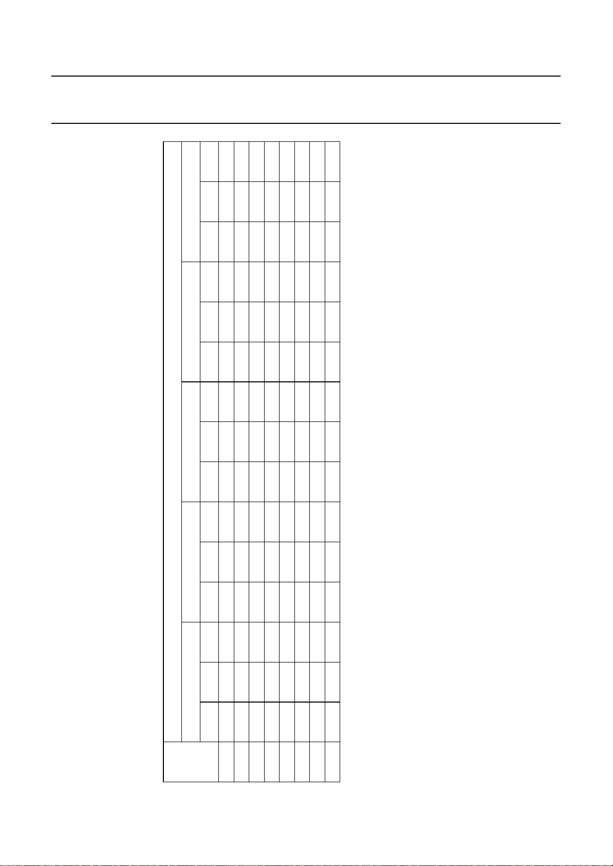
(2)
[0] 1
n-1
[1] S
n-1
[2] 1 S
[0] 1 X X 0
n-1
n-1
[3] S
[1] S
n-1
n-1
[3]1S
[1]1S
n-1
n-1
[4] S
[2] S
n-1
n-1
[0] 1
[1] S
[2] 1 S
[3] S
[4] 1 S
[0] S
n
n
n
n
n
n-1
[0] 1 X X 0
n
[1] S
n
[2] 1 S
[0] 1 X X 0 X X 0
n
n
[3] S
[1] S
n
n
QUADRATURE AMPLITUDE MODULATION
[4]1S
[2]1S
[0]1XX0XX0XX0
[4] 1 S
n-1
n-1
n-1
[5] S
[3] S
[1] S
n-1
n-1
n-1
[6]1S
[4]1S
[2]1S
n-1
n-1
n-1
n
[5] S
n
[0]1XX0XX0XX0XX0
[6] 1 S
n
n-1
256 QAM 64 QAM 32 QAM 16 QAM 4 QAM
[7] S
[5] S
[3] S
[1] S
[7] S
n
n-1
3S
4S
FUNCTIONAL DESCRIPTION
Input interface (see Fig.3)
The received input data stream is a sequence which is interpreted as a stream of bytes. The bits are assumed to be non-byte aligned and sent in
MSB to LSB order. New data may be present at the input pins on each rising edge of the master clock input (CLK). Valid data is indicated by
VALI = HIGH. When VALI = LOW the data is not valid and will be neglected. There are no limitations imposed on valid/non-valid sequences.
The Quadrature Amplitude Modulation (QAM) of the input data is given in Table 1.
Table 1 Quadrature amplitude modulation; note 1
SLOT
n-1
DATA1 DATA0 VALI DATA1 DATA0 VALI DATA1 DATA0 VALI DATA1 DATA0 VALI DATA1 DATA0 VALI
1S
0S
n-1
n-1
2S
1996 Jul 17 6
[2] 1 S
[0] 1 S
n
n
[3] S
[1] S
n
n
[4] 1 S
[2] 1 S
[0]1XX0XX0XX0XX0
n
n
n
[5] S
[3] S
[1] S
n
n
n
5S
6S
7S
Notes
1. X = don’t care.
2. The numbers given in parenthesis refer to the bit numbers.
 Loading...