

Philips SAA7206H Datasheet

INTEGRATED CIRCUITS
DATA SH EET
SAA7206H
DVB compliant descrambler
Product specification
Supersedes data of 1996 Oct 02
File under Integrated Circuits, IC02
1996 Oct 09

Philips Semiconductors Product specification
DVB compliant descrambler SAA7206H
CONTENTS
1 FEATURES
2 GENERAL DESCRIPTION
3 ORDERING INFORMATION
4 QUICK REFERENCE DATA
5 BLOCK DIAGRAM
6 PINNING
7 FUNCTIONAL DESCRIPTION
7.1 MPEG-2 systems parsing
7.2 PES level descrambling
7.3 Descrambler core
7.4 Microcontroller interface
7.5 Output interfacing
7.6 Boundary scan test
7.7 Programming the descrambler
8 LIMITING VALUES
9 HANDLING
10 THERMAL CHARACTERISTICS
11 DC CHARACTERISTICS
12 AC CHARACTERISTICS
13 PACKAGE OUTLINE
14 SOLDERING
14.1 Introduction
14.2 Reflow soldering
14.3 Wave soldering
14.3.1 QFP
14.3.2 SO
14.3.3 Method (QFP and SO)
14.4 Repairing soldered joints
15 DEFINITIONS
16 LIFE SUPPORT APPLICATIONS
1996 Oct 09 2

Philips Semiconductors Product specification
DVB compliant descrambler SAA7206H
1 FEATURES
• Input data fully compliant with the Transport Stream
(TS) definition of the MPEG-2 systems specification
• Input data signals; [Forward Error Correction (FEC)
Interface]
– modem data input bus (8-bit wide)
– valid input data indicator
– erroneous packet indicator
– first packet byte indicator
– byte strobe signal (for asynchronous mode only).
The interface can be programmed to one of two modes:
– Asynchronous mode; byte strobe input signal
(MBCLK) < 9 MHz, for connection to a modem (FEC)
– Synchronous mode; MBCLK is not used. Data is
delivered to the descrambler synchronized with the
chip clock (DCLK) [9 MHz (typ.) with a 33% duty
cycle].
• No external memory
• Effective bit rate; f
• Control interface; 8-bit multiplexed data/address,
memory mapped I/O (90CE201 microcontroller parallel
bus compatible), in combination with a microcontroller
interrupt signal (IRQ)
• Output ports are identical to the input data interface
(demultiplexer interface)
– except for the packet error indicator (MB/MB), as the
descrambler translates an active MB signal to the
‘transport_error_indicator’ bit in the transport stream
– except for the byte strobe input signal (MBCLK), as
data is delivered to the demultiplexer, synchronized
with the descrambler chip clock which is generated
by the demultiplexer
≤ 72 MHz
bit
• Descrambler, based on the super descrambler
mechanism algorithm with stream decipher and block
decipher. The descrambler is initialized with a 64-bit
Control Word (CW) at the beginning of a transport
stream packet payload of a selected Packet
Identification (PID). The descrambler operates on
transport stream packet or Packetized Elementary
Stream (PES) packet payloads
• Microcontroller support; only for control, no specific
descrambling tasks are performed by the
microcontroller. However, parsing and processing of
conditional access information (such as EMM and ECM
data) is left to the system microcontroller
• Boundary scan test port for boundary scan.
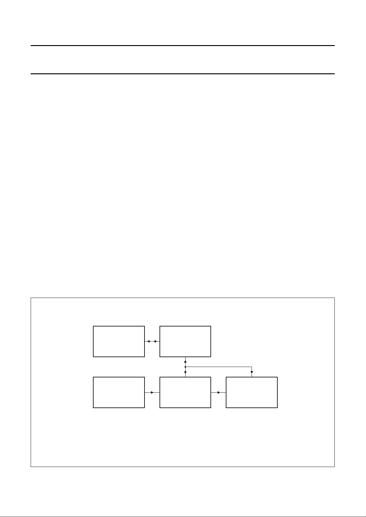
2 GENERAL DESCRIPTION
The SAA7206H (DVB compliant) is designed for use in
MPEG-2 based digital TV receivers, incorporating
conditional access filters. Such receivers are to be
implemented in, for instance, a digital video broadcasting
top set box, or an integrated digital TV receiver.
An example of a demultiplexer/descrambler system
configuration, containing a channel decoder module, a
demultiplexer, a system controller and a conditional
access system is shown in Fig.3. The main function of the
descrambler is to descramble the payloads of MPEG-2 TS
packets or PES packets. In addition, the descrambler
retrieves Conditional Access (CA) data [such as
Entitlement Management Messages (EMM) and
Entitlement Control Messages (ECM) etc.] from the stream
and passes it to the system microcontroller for processing.
3 ORDERING INFORMATION
PACKAGE
TYPE NUMBER
NAME DESCRIPTION VERSION
SAA7206H QFP64 plastic quad flat package; 64 leads (lead length 1.95 mm);
body 14 × 20 × 2.8 mm
1996 Oct 09 3
SOT319-2
Philips Semiconductors Product specification
DVB compliant descrambler SAA7206H
4 QUICK REFERENCE DATA
SYMBOL PARAMETER CONDITIONS MIN. TYP. MAX. UNIT
V
DDD
V
DDD(core)
P
tot
f
clk
T
amb
5 BLOCK DIAGRAM
digital supply voltage −−5.5 V
digital supply voltage for core −−3.6 V
total power dissipation V
DDD(core)
V
DDD
= 3.3 V,
=5V, CL=15pF
−−250 mW
clock frequency duty cycle = 30 to 55% −−9 MHz
operating ambient temperature 0 − 70 °C
handbook, full pagewidth
TDI
TCK
TMS
TRST
TDO
DAT7
to
DAT0
DCS
R/W
A1
A0
IRQ
V
DDD(core)
V
DDD1
to
V
DDD9
18
19
20
46
37
7 to 9,
12 to 16
3
63
4
5
1
36
6, 11, 21, 26,
32, 41, 51, 57, 64
TC1 TC0
61 60
TEST CONTROL BLOCK
BOUNDARY SCAN TEST
FOR
AND
SCAN TEST
SAA7206
MICROCONTROLLER
INTERFACE
CONDITIONAL
ACCESS
FILTERS
2, 17, 23, 27,
33, 52, 58
V
to V
SSD1
SSD7
V
SSD1(core)
V
SSD2(core)
MIN7 to MIN0
47 to 50,
53 to 56
TRANSPORT STREAMS
PACKET
IDENTIFICATION
BANK
STREAM
DECIPHER
10, 42
,
MB/MB
MDV
44 45 43 59
AND
AF PARSER
OUTPUT
INTERFACE
MBCLK
MSYNC
CONTROL
WORD
BANK
BLOCK
DECIPHER
24, 25,
28 to 31,
34, 35
MGG313
22
DCLK
62
POR
40
OE
DATO0
to
DATO7
38
DVO
39
SYNCO
Fig.1 Block diagram.
1996 Oct 09 4

Philips Semiconductors Product specification
DVB compliant descrambler SAA7206H
6 PINNING
SYMBOL PIN I/O DESCRIPTION
IRQ 1 O interrupt request output for microcontroller (active LOW, open-drain output)
V
SSD1
DCS 3 I descrambler chip select input (active LOW)
A1 4 I A1 = address/data indicator input
A0 5 I A0 = MSByte indicator input
V
DDD1
DAT7 7 I/O microcontroller bidirectional data bus bit 7
DAT6 8 I/O microcontroller bidirectional data bus bit 6
DAT5 9 I/O microcontroller bidirectional data bus bit 5
V
SSD1(core)
V
DDD2
DAT4 12 I/O microcontroller bidirectional data bus bit 4
DAT3 13 I/O microcontroller bidirectional data bus bit 3
DAT2 14 I/O microcontroller bidirectional data bus bit 2
DAT1 15 I/O microcontroller bidirectional data bus bit 1
DAT0 16 I/O microcontroller bidirectional data bus bit 0
V
SSD2
TDI 18 I boundary scan test data input
TCK 19 I boundary scan test clock input
TMS 20 I boundary scan test mode select input
V
DDD3
DCLK 22 I 9 MHz descrambler chip clock input (duty cycle range: 30 to 55%)
V
SSD3
DATO0 24 O data output to demultiplexer bit 0
DATO1 25 O data output to demultiplexer bit 1
V
DDD4
V
SSD4
DATO2 28 O data output to demultiplexer bit 2
DATO3 29 O data output to demultiplexer bit 3
DATO4 30 O data output to demultiplexer bit 4
DATO5 31 O data output to demultiplexer bit 5
V
DDD5
V
SSD5
DATO6 34 O data output to demultiplexer bit 6
DATO7 35 O data output to demultiplexer bit 7
V
DDD(core)
TDO 37 O boundary scan test data output
DVO 38 O valid output data indicator
SYNCO 39 O indicates the first output byte (sync) of a transport packet
2 GND digital ground 1
6 supply digital supply voltage 1 (+5 V)
10 GND digital ground 1 for core
11 supply digital supply voltage 2 (+5 V)
17 GND digital ground 2
21 supply digital supply voltage 3 (+5 V)
23 GND digital ground 3
26 supply digital supply voltage 4 (+5 V)
27 GND digital ground 4
32 supply digital supply voltage 5 (+5 V)
33 GND digital ground 5
36 supply digital supply voltage for core (+3.3 V)
1996 Oct 09 5

Philips Semiconductors Product specification
DVB compliant descrambler SAA7206H
SYMBOL PIN I/O DESCRIPTION
OE 40 I output enable (active LOW), if HIGH, device outputs are high impedance,
(connected to logic 0 in normal operation)
V
DDD6
V
SSD2(core)
MSYNC 43 I indicates the first input byte (sync) of a transport packet
MDV 44 I valid input data indicator
MB/MB 45 I packet error indicator input (programmable polarity)
TRST 46 I boundary scan reset input (LOW in normal operation)
MIN7 47 I 8-bit wide modem data input bit 7
MIN6 48 I 8-bit wide modem data input bit 6
MIN5 49 I 8-bit wide modem data input bit 5
MIN4 50 I 8-bit wide modem data input bit 4
V
DDD7
V
SSD6
MIN3 53 I 8-bit wide modem data input bit 3
MIN2 54 I 8-bit wide modem data input bit 2
MIN1 55 I 8-bit wide modem data input bit 1
MIN0 56 I 8-bit wide modem data input bit 0
V
DDD8
V
SSD7
MBCLK 59 I byte strobe input signal < 9 MHz
TC0 60 I test control input 0 (not connected in normal operation)
TC1 61 I test control input 1 (not connected in normal operation)
POR 62 I power-on reset, must be active HIGH during at least 5 DCLK pulses
W 63 I read/write input selection
R/
V
DDD9
41 supply digital supply voltage 6 (+5 V)
42 GND digital ground 2 for core
51 supply digital supply voltage 7 (+5 V)
52 GND digital ground 6
57 supply digital supply voltage 8 (+5 V)
58 GND digital ground 7
64 supply digital supply voltage 9 (+5 V)
1996 Oct 09 6

Philips Semiconductors Product specification
DVB compliant descrambler SAA7206H
handbook, full pagewidth
V
SSD1
V
DDD1
DAT7
DAT6
DAT5
V
SSD1(core)
V
DDD2
DAT4
DAT3
DAT2
DAT1
DAT0
V
SSD2
IRQ
DCS
A1
A0
TDI
TCK
DDD9
V
R/W
POR
TC1
TC0
64
63
62
61
60
1
2
3
4
5
6
7
8
9
10
11
12
13
14
15
16
17
18
19
20
21
22
23
24
TMS
DDD3
V
DCLK
SSD3
V
DATO0
SSD7VDDD8
MBCLK
V
59
58
SAA7206
25
26
DDD4
DATO1
V
57
27
SSD4
V
MIN0
56
28
DATO2
MIN1
55
29
DATO3
MIN2
54
30
DATO4
MIN3
V
53
31
DATO5
SSD6
52
32
DDD5
V
51
50
49
48
47
46
45
44
43
42
41
40
39
38
37
36
35
34
33
MGG312
V
DDD7
MIN4
MIN5
MIN6
MIN7
TRST
MB/MB
MDV
MSYNC
V
SSD2(core)
V
DDD6
OE
SYNCO
DVO
TDO
V
DDD(core)
DATO7
DATO6
V
SSD5
Fig.2 Pin configuration.
1996 Oct 09 7
Philips Semiconductors Product specification
DVB compliant descrambler SAA7206H
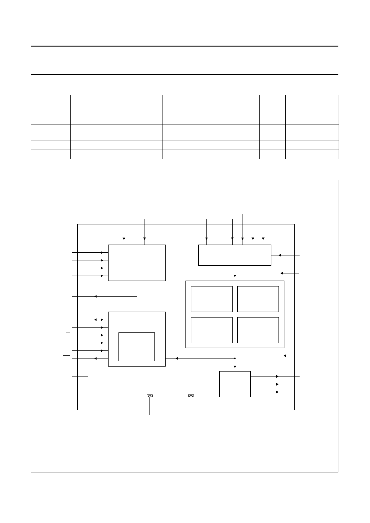
7 FUNCTIONAL DESCRIPTION
A block diagram of the internal structure of the
descrambler (DVB compliant) is illustrated in Fig.1.
The block diagram illustrates the main functional modules
in the descrambler. The modules are as follows:
• The MPEG-2 syntax parser, which parses transport
streams that comply with the MPEG-2 systems
specification
• The descrambler module consisting of:
– A Packet Identification (PID) bank containing 6 PID
values of the streams selected for descrambling.
All bits of PID5 (address 0x0205) can be masked
individually with PID5_mask (address 0x0209), to
enable multiple PID selection.
– A Control Word (CW) bank containing 6 CW pairs
and a default CW. A CW pair consists of
2 descrambler control words (odd and even), each
word with a length of 64 bits.
– The descrambler core containing the actual
descrambler with the stream cipher and the block
cipher module.
• A microcontroller interface providing protocol handling
for the memory mapped I/O control bus
(Philips 90CE201 compatible). This module contains an
interrupt request handler and data filters for the retrieval
of Conditional Access (CA) information:
• The CA filters select data on the basis of PIDs, and a
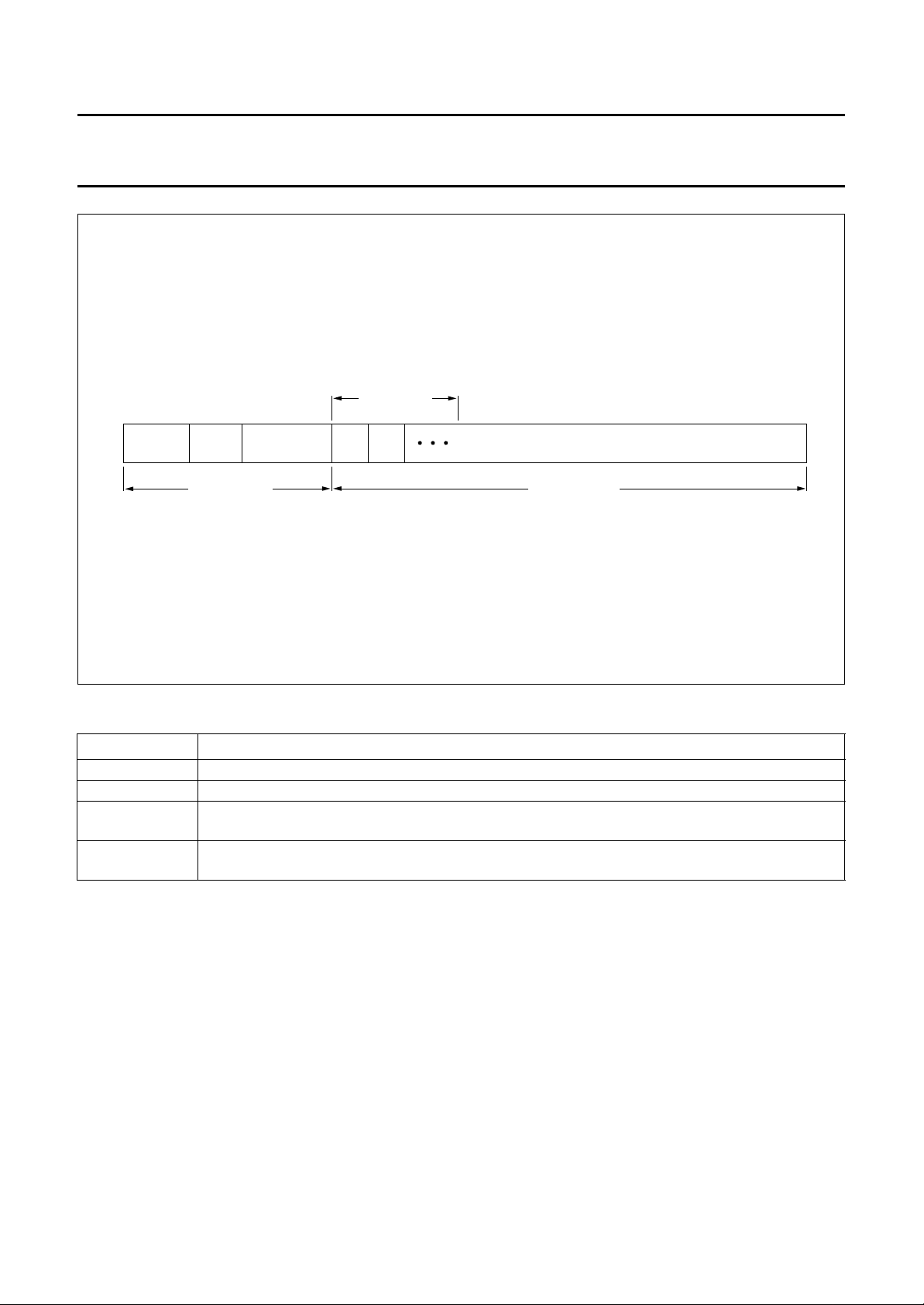
combination of MPEG-2 section addressing fields.
Selected CA data is stored in eighteen 256 byte
(constrained random access) buffers which can be read
by the microcontroller. The CA message section has a
maximum length of 256 bytes. It consists of a 3 bytes
long header with Table_id and section_length data.
The remaining part of the CA message are the
CA_data_bytes (see Fig.4). If a section is longer than
256 bytes, the data capture is stopped (with an interrupt
to the microcontroller) after 256 bytes are in the buffer
and the ‘section_to_long’ bit is set. The filters are
capable of monitoring 18 CA streams (containing EMM
and ECM data) simultaneously. Two different lengths
are used for address filtering:
– 16 filters where the first 7 bytes of the CA_data_bytes
field are used for address filtering
– 2 (DVB compliant) filters where the first 17 bytes of
the CA_data_bytes field are used for address filtering
– A chip identification byte (value 0x02) can be read by
the software from address 0x0003 (see Table 10).
handbook, full pagewidth
CONDITIONAL
ACCESS
SYSTEM
DEMODULATOR
AND
FORWARD ERROR
CORRECTOR
MICRO-
CONTROLLER
DESCRAMBLER
(SAA7206H)
Fig.3 Demultiplexer system configuration.
1996 Oct 09 8
DVB
DEMULTIPLEXER
(SAA7205)
MGG314
Philips Semiconductors Product specification
DVB compliant descrambler SAA7206H
handbook, full pagewidth
table_id reserved section length byte 0 byte 1
section header
(3 bytes)
7 or 17 bytes
of filtering
CA_data_bytes
[253 bytes (max.)]
section payload
[253 bytes (max.)]
MGG316
Fig.4 Syntax of the conditional access message.
Table 1 Explanation of Fig.4
SYNTAX DESCRIPTION
Table_id 8-bit field for identification
Reserved 4-bit field with section_syntax_indicator (1 bit), DVB_reserved (1 bit) and ISO_reserved (2 bits)
Section_length 12-bit field that specifies the number of bytes that follow the section_length field up to the end of
the section
CA_data_byte 8-bit field that carries private CA information. Up to the first 17 CA_data_bytes may be used for
address filtering
1996 Oct 09 9

Philips Semiconductors Product specification
DVB compliant descrambler SAA7206H
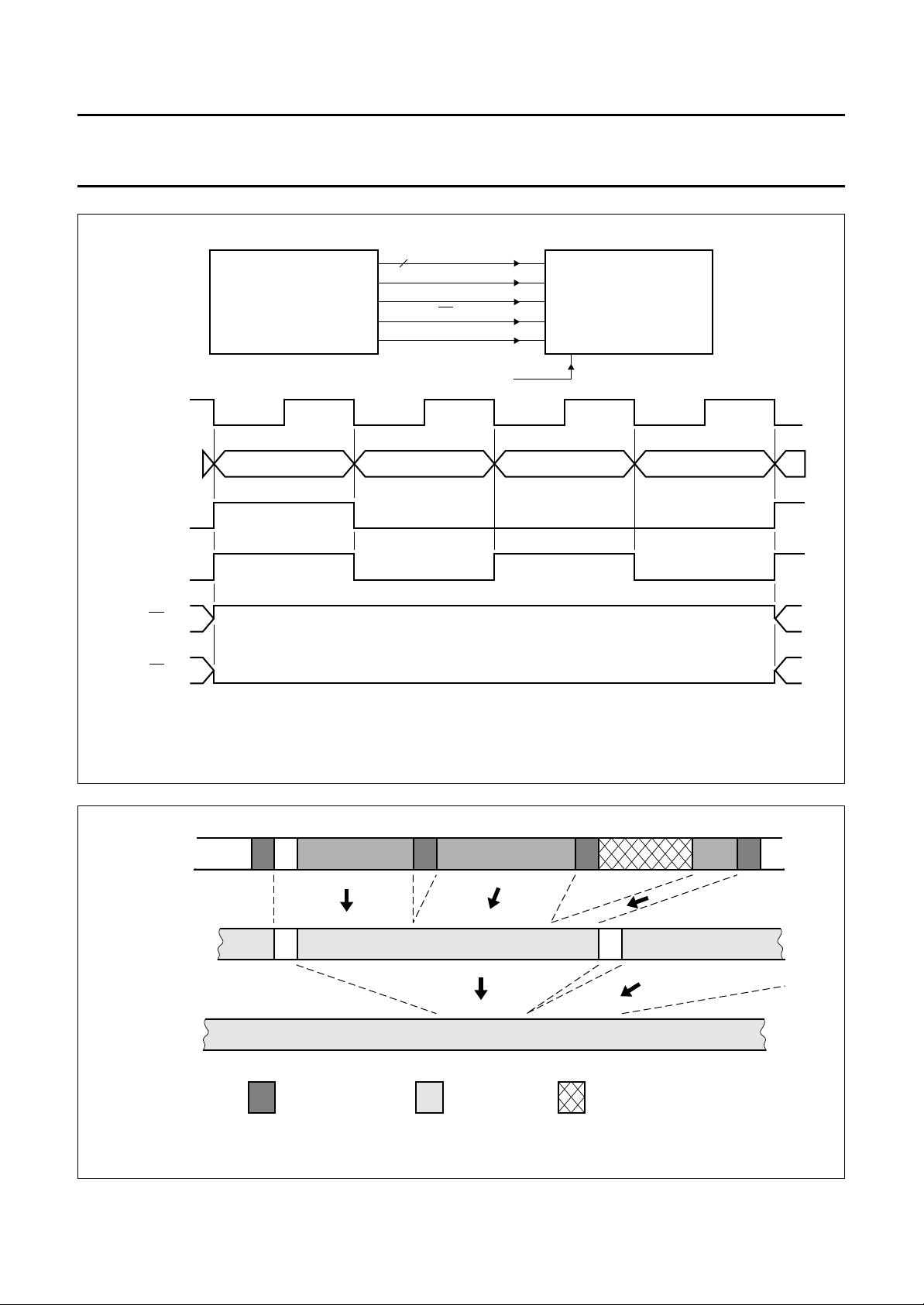
7.1 MPEG-2 systems parsing
The descrambler receives data from a Forward Error
Correction (FEC) decoder (see Fig.5) in a digital TV
receiver, in the following input data format:
• 8 data bits via MIN7 to MIN0.
• A valid input data indicator signal (MDV), which is HIGH
for consecutive valid bytes and output by either a FEC
decoder or a descrambler. Consequently the
descrambler input data is allowed to have a ‘bursty’
nature.
• A transport packet error indicator (
HIGH for the duration of each 188 byte transport packet
in which the FEC decoder found more errors than it
could correct. The polarity (active HIGH or LOW) of the
error indicator is programmable [bit ‘Bad_polarity’
(see Table 10, address 0x0100)].
• A packet sync signal (MSYNC) which goes HIGH at the
start of the first byte of a transport packet. Only the rising
edge of MSYNC is used for synchronization, the exact
HIGH time of the signal is therefore irrelevant.
• A byte strobe signal (MBCLK; < 9 MHz) which indicates
consecutive data bytes in the input stream, in the non
9 MHz mode only [bit ‘9 MHz_interface’ = 0
(see Table 10, address 0x0100)]. MBCLK is used as an
enable signal, and transport stream input bytes are
sampled on its rising edges. If the input interface is
programmed to the 9 MHz mode
(‘9 MHz_interface’ = 1), the MBCLK signal is ignored
and bytes are latched on rising edges of the DCLK.
• A descrambler clock signal (DCLK; 9 MHz; duty cycle
range 30 to 55%) which is the processing clock for the
descrambler IC. If rising edges of this signal are used to
input data to the descrambler, the 9 MHz mode must be
programmed (bit ‘9 MHz_interface’ = 1, see Table 10,
address 0x0100).
MB/MB) which is
The hierarchical multiplex level below the MPEG-2
transport stream is the packetized elementary stream.
The PES header is only parsed partially by the DVB
descrambler to locate its scrambling control bits. Parsing is
performed for all incoming transport packets, and the
parser is synchronized to a rising edge on its MSYNC
input. A microcontroller can compose a set of 6 PIDs by
programming the appropriate registers in the PID filter
bank within the descrambler.
These PIDs identify the packets of the streams that are to
be descrambled. All 13 bits of PID5 (see Table 10,
address 0x0205) can be individually enabled/disabled with
a mask of 13 bits (see Table 10, address 0x0209) to
enable multiple PID selection. The PIDs of PES scrambled
packets must be indicated by programming a logic 1 to the
corresponding bit of the ‘PIDi_is_pes’ word
(see Table 10, address 0x0206).
MPEG-2 multiplex fields which are related to CA
information, in so called sections, are parsed only partly.
CA sections containing for instance Entitlement
Management Messages (EMM) and Entitlement Control
Messages (ECM) etc. are retrieved from the stream and
stored in 256 byte buffers in the CA filter module. For the
selection of CA data, 18 additional PIDs and section
header information (table_id, address field, both with bit
masks) can be programmed. All 13 bits of PID filters
16 and 17 can be individually enabled/disabled with a
mask of 13 bits (see Table 10, addresses 0x03A6
and 0x03BA) to enable multiple PID selection for CA
messages. A microcontroller may access data in the
256 byte CA buffers (each filter has its own buffer thus
18 in total) for software based parsing and processing.
The parser module in the descrambler parses transport
streams compliant to the MPEG-2 systems syntax.
MPEG-2 systems specifies a hierarchical two-level
multiplex (see Fig.6). The top hierarchical level is the
transport stream, consisting of relatively short (188 byte)
transport packets. Each transport packet consists of a
4 byte transport header, an optional adaptation field and a
payload. The transport header contains a 13-bit PID field.
The adaptation field may contain Program Clock
Reference (PCR) data and transport private data, among
others. Both transport header and optional adaptation
fields are parsed by the TS parser module.
1996 Oct 09 10
Philips Semiconductors Product specification
DVB compliant descrambler SAA7206H
8
handbook, full pagewidth
FEC
MBCLK
MIN7 to MIN0
MBCLK
MDV
MB/MB
MSYNC
DESCRAMBLER
DCLK
MIN7 to MIN0
MSYNC
MDV
MB/MB
MB/MB
handbook, full pagewidth
transport
stream
message invalid data
error-free transport packet (programmable polarity)
erroneous transport packet
message invalid data
Fig.5 Signal constellation FEC decoder - descrambler Interfacing.
MGG317
packetized
elementary
stream
elementary
stream
= transport_header = pes_header = stuffing
Fig.6 MPEG-2 two level hierarchical demultiplexing.
1996 Oct 09 11
MGG318

Philips Semiconductors Product specification
DVB compliant descrambler SAA7206H
7.2 PES level descrambling
PES level descrambling is possible in accordance with the
recommendations of the DVB standard with the DVB
descrambler IC. The actual restrictions however, required
by the DVB descrambler IC, are less strict than to the
recommendations in the DVB standard. The restrictions
for PES level descrambling imposed by the IC are as
follows:
• Scrambling shall only occur at one level (TS or PES) and
is not allowed to occur at both levels simultaneously
• The complete PES header must be present in exactly
one TS packet. Consequently, the size of a PES packet
header shall not exceed 184 bytes
• Only the PES packet data bytes (PES payload) are
descrambled
• TS packets resulting from scrambling at PES level are
not chained and thus are independent. Consequently,
the internal descrambler algorithms (stream decipher
and block decipher) are initialized at the start of each
(PES scrambled) TS packet payload.
In order to be able to distinguish between sections and
PES packets, a PID for a PES scrambled packet is
indicated by programming the according ‘PIDi_is_pes’ bit
(see Table 10, address 0x0206) to logic 1. If the
payload_unit_start_indicator bit is set in the TS packet
header and the ‘PIDi_is_pes’ bit is set for a particular PID,
the PES scrambling control bits, which are present in the
PES header, are stored in the accessible ‘pes_sc_PIDi’
register (see Table 10, address 0x0208).
Descrambling at TS level always has priority over
descrambling at PES level. Consequently, PES level
descrambling is only possible when the
transport_scrambling_control bits in the TS header are
‘00’. In that situation the payload of the PES packets is
descrambled using the scrambling control bits of the
‘pes_sc_PIDi’ register.
Remark: PID masking (for PID5) should not be combined
with PES level descrambling. Only one pair of PES
scrambling control bits per PID is stored in an Internal
register. Thus interleaving of PES messages, which can
occur in the situation of multiple PID selection, can give the
wrong descrambling result. As a consequence the
microcontroller must program the ‘PID5_is_pes’ bit
(see Table 10, address 0x0206) to logic 0 when multiple
PID selection is used.
7.3 Descrambler core
The descrambler core consists of three modules:
• A PID filter which selects packets for descrambling
• A control word bank containing 6 sets (odd and even) of
control words and a Default Control Word (DCW)
• The super descrambler core with the implementation of
the stream decipherment and the block decipherment
algorithms.
The PID filter contains 6 registers which hold data in the
format indicated in Fig.7. Six individual PIDs are stored to
identify 6 packet streams. All bits of PID5 (see Table 10,
address 0x0205) can be masked with the ‘PID5_mask’
(see Table 10, address 0x209), to enable descrambling on
multiple PIDs. To disable a bit of PID5 with the
‘PID5_mask’ a logic 0 must be programmed. After a
power-on reset pulse all mask bits are preset to logic 1.
To each PID a 3-bit Control Word Pair Index pointer
(CWPI) is attached. A CWPI prescribes which control word
pair, consisting of odd and even control words, has to be
used to initialize the DVB descrambler for payloads of
packets with the associated PID. After a power-on reset all
CWPIs are set to ‘111’ to enable a correct initialization of
the conditional access system.
If two or more programmed PIDs match the PID of the TS
packet at the same time (while the CWPI value of the
programmed PIDs is not equal to ‘110’ or ‘111’), the
programmed PID with the lower index number has a higher
priority. However, the default control word, when enabled,
has the highest priority.
Thus, the built-in priority (HIGH-to-LOW transition) for the
programmed PIDs is; DCW, PID0, PID1, PID2, PID3, PID4
and PID5.
A 2-bit scrambling_control field is present in the TS packet
header and in the PES header (ts_sc1 and ts_sc0 and
pes_sc1 and pes_sc0 respectively). The bits in this
header field indicate whether the TS packet or PES
payload is scrambled or not. In addition, these bits also
indicate which control word (odd or even) of a control word
pair was used to initialize the DVB descrambler, as
indicated in Tables 2 and 3.
1996 Oct 09 12

Philips Semiconductors Product specification
DVB compliant descrambler SAA7206H
If the payload of a packet is descrambled, the descrambler
subsequently resets the scrambling_control bits in the TS
or PES header (to ‘00’). For each of the 6 PIDs in the PID
filter bank the values of the TS scrambling_control bits are
stored in a microcontroller accessible register, prior to
descrambling [bits: ‘ts_sc_PIDi1’ and ‘ts_sc_PIDi0’;
(see Table 10, address 0x0208), ‘i’ is in the range 5 to 0].
For each of the 6 PIDs in the PID filter bank, of which the
corresponding PIDi_is_pes bit (see Table 10,
address 0x0206) is also set to logic 1, the values of the
PES scrambling_control bits are stored in a
microcontroller accessible register, prior to descrambling
[bits:‘pes_sc_PIDi1’ and ‘pes_sc_PIDi0’ (see Table 10,
address 0x0208) ‘i’ is in the range 5 to 0]. TS and PES
scrambling_control retrieval is independent of the value of
the CWPI.
Table 2 Definition of the bits in the PES
scrambling_control field
VALUE DESCRIPTION
00 data is not scrambled
01 data is not scrambled
10 data is scrambled with the EVEN control
word
11 data is scrambled with the ODD control
word
Remark: The payloads of packets with TS
scrambling_control bits equal to ‘01’ are descrambled
using the default control word, regardless of their PID
and/or CWPI values. Thus, even PIDs which are not
programmed in the PID filter bank are descrambled with
the DCW should transport_scrambling_control = ‘01’.
For PIDs in the PID filter bank, if
transport_scrambling_control = ‘01’, the payload is
descrambled with the default control word, regardless of
the value of the associated CWPI. If the default CW is
invalid however [‘DCW_valid’ = 0 (see Table 10,
address 0x0206)], DCW based descrambling is disabled.
Descrambling using the DCW is only possible on TS
packet level.
The control word bank contains storage space for 6 control
word pairs and a default control word. A control word pair
consists of 2 CWs and an odd and even CW, as indicated
in Table 4. A control word contains 64 bits. In conjunction
with the control word selection mechanism given in
Table 4, the CW bank allows any CW pair to be used with
any PID. All PIDs may, therefore, use their own specific
CW pair, but all of them may also share one CW pair.
The super descrambler algorithm is implemented in the
core of the descrambler. Descrambling is performed on
the payload of a transport packet or a PES. The transport
header, the (optional) adaptation field and the PES header
are excepted.
Table 3 Definition of the bits in the TS
scrambling_control field
VALUE DESCRIPTION
00 data is not scrambled
01 data is scrambled with the default control
word
10 data is scrambled with the EVEN control
word
11 data is scrambled with the ODD control
word
1996 Oct 09 13
Philips Semiconductors Product specification
DVB compliant descrambler SAA7206H
Table 4 Descrambler control word storage; see Table 10
CONTROL WORD (128 BITS) ADDRESS
Control word 0 odd Control word 0 even 0x1000 to 0x1007
Control word 1 odd Control word 1 even 0x1008 to 0x100F
Control word 2 odd Control word 2 even 0x1010 to 0x1017
Control word 3 odd Control word 3 even 0x1018 to 0x101F
Control word 4 odd Control word 4 even 0x1020 to 0x1027
Control word 5 odd Control word 5 even 0x1028 to 0x102F
Default control word − 0x1030 to 0x1033
handbook, full pagewidth
See Table 10 for details.
15
PID_0
PID_5
15
15
15
15
12 11
121211
13
6721
PID5_is_pes to PID0_is_pes
ts_sc_PID5[1..0] to ts_sc_PID0[1..0]
pes_sc_PID5[1..0] to pes_sc_PID0[1..0]
PID5_mask
3
2
CWPI_0
CWPI_5
DCW_valid
MGG319
Fig.7 Syntax and definition of PID and control word pair Index.
0
0x0200 - W
0x0205 - W
0
0x0206 - W
0x0207 - R
0x0208 - R
0x0209 - W
Table 5 CWPI values; see Fig.7
CWPI VALUE DESCRIPTION
0 0 0 select control word pair 0
0 0 1 select control word pair 1
0 1 0 select control word pair 2
0 1 1 select control word pair 3
1 0 0 select control word pair 4
1 0 1 select control word pair 5
1 1 0 DO NOT descramble
1 1 1 DO NOT descramble
1996 Oct 09 14
Philips Semiconductors Product specification
DVB compliant descrambler SAA7206H
7.4 Microcontroller interface
The microcontroller interface provides a means of
communication between a system controller (for instance
“Philips 90CE201”
) in a digital TV receiver and the
descrambler internal registers and buffers. The physical
interface consists of:
• DAT7 to DAT0; an 8-bit wide bidirectional data bus.
Data and address information are multiplexed on this
bus.
• DCS; an active LOW chip select signal.
The descrambler only responds to microcontroller
communication if this signal is driven LOW.
W; an active HIGH read signal, indicating that the
• R/
microcontroller is attempting to read data from registers
or buffers inside the descrambler. If this signal is LOW,
data is being written to registers or buffers inside the
descrambler.
• A1 and A0; a 2-bit address bus. If the least significant
address bit (0) is logic 0, the most significant byte of a
16-bit register is addressed, otherwise the least
significant byte is selected. If the most significant
address bit (1) is logic 1 DAT7 to DAT0 carries the
address information, otherwise it will carry control data.
• IRQ; an active LOW (open-drain output) interrupt
request signal. An interrupt is set if one of the15 bits in
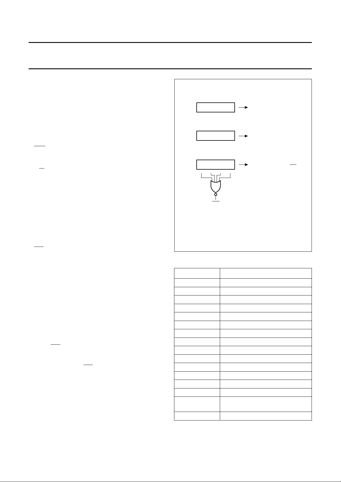
the descramblers internal interrupt register is set.
The interrupt mechanism consists of three 15-bit
registers and one 4-bit register, as illustrated in Fig.8.
The interrupt status register enables the microcontroller
to monitor the momentary status of the interrupts.
This is particularly useful during read operations in the
descramblers CA buffers, as the interrupt status bits in
question [‘flt0_stat’, ‘flt1_stat’, etc. (see Table 10,
addresses 0x0002 and 0x0004)] are reset when the
buffers have been emptied or released.
The interrupt mask register (see Table 10,
address 0x0001) prevents individual interrupts from
resetting IRQ (to logic 0). The interrupt status bits are
logically ANDed with the mask. If a rising edge occurs on
one of the resulting signals, it is latched into the interrupt
register, thus resetting IRQ.
handbook, halfpage
The interrupt register is reset when addressed.
0x0002/0x0004
(read only)
19-bit status
0x0001
(write only)
15-bit mask
0x0000
(read/write)
15-bit interrupt
IRQ
momentary status of the
individual interrupt bits
enables/disables
individual interrupts
latched interrupts, indicating
which interrupt(s) set IRQ
MGG320
Fig.8 Descrambler version 3, microcontroller
interrupt mechanism.
Table 6 Definition of interrupt mechanism; see Fig.8
BIT NUMBER MEANING OF INTERRUPT
0 filter 0 retrieved CA data
1 filter 1 retrieved CA data
2 filter 2 retrieved CA data
3 filter 3 retrieved CA data
4 filter 4 retrieved CA data
5 filter 5 retrieved CA data
6 filter 6 retrieved CA data
7 filter 7 retrieved CA data
8 filter 8 retrieved CA data
9 filter 9 retrieved CA data
10 filter 10 retrieved CA data
11 filter 11 retrieved CA data
12 filter 12 retrieved CA data
13 filter 13 retrieved CA data
14 filter 14, 15, 16 or 17 retrieved
CA data
15 empty
1996 Oct 09 15
Philips Semiconductors Product specification
DVB compliant descrambler SAA7206H
The interrupt register itself is reset
(to 0000000000000000) as soon as it is addressed
(0x0000) by the microcontroller.
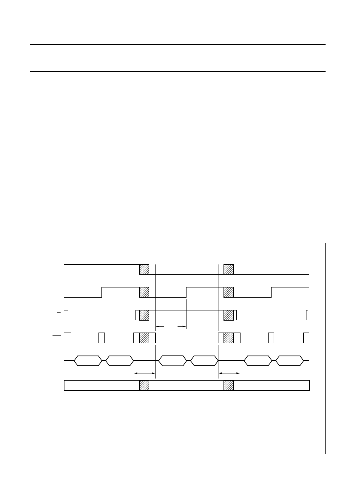
A typical example of communication between
microcontroller and descrambler is illustrated in Fig.9.
The descrambler contains an auto increment address
counter which can be loaded by performing a write
address operation. The present operation, whether read or
write, is now performed on the current address. The next
operation, whether read or write, is performed on the
current address plus 1.
Remark: Avoid resetting the auto increment address
counter to 0x0000, when not handling interrupts, as
addressing it causes the interrupt register to be reset.
Consequently, interrupt information might be lost.
The descrambler internal register and buffer addresses
are organized as illustrated in Fig.10. The first 4 address
bits (15 to 12) are used to select either the descrambler
registers (equals 0) or one of the descrambler buffers
(ranges 1 and 2).
In the buffer mode, the remaining address bits (11 to 0) are
part of the word address (range depending on the buffer,
see Table 10). In the register mode, bits 11 to 8 specify
the register unit number (see Fig.10). The remaining 8 bits
of the address (7 to 0) indicate specific register addresses
within a selected unit. The address range in a specific
register unit depends on the number of registers present
and is different for each unit. For details refer to Table 10.
The CA filter module in the microcontroller interface unit is
capable of accessing general CA messages (ECM and
EMM, etc.) in the transport stream. The CA filter module
consists of 18 filters and 18 buffers of 256 bytes each,
thus each filter has its own data buffer. The 18 filters are
divided into two types of filters, which are specified in
Table 9. For each filter the ‘table_id’ of the section (the first
byte of the section see Fig.9), can be masked.
The architecture of the 9 CA filter pairs is shown in Fig.11.
handbook, full pagewidth
A1
A0
R/W
DCS
DAT7 to
DAT0
The descrambler internal register address is incremented automatically.
MSByte LSByte MSByte LSByte MSByte LSByte
>666 ns >666 ns
write address N read data @ N write data @ N+1
>24 ns
MGG321
Fig.9 Microcontroller descrambler communication (example).
1996 Oct 09 16
 Loading...