

Philips SAA7205H Datasheet

INTEGRATED CIRCUITS
DATA SH EET
SAA7205H
MPEG-2 systems demultiplexer
Preliminary specification
File under Integrated Circuits, IC02
1997 Jan 21

Philips Semiconductors Preliminary specification
MPEG-2 systems demultiplexer SAA7205H
CONTENTS
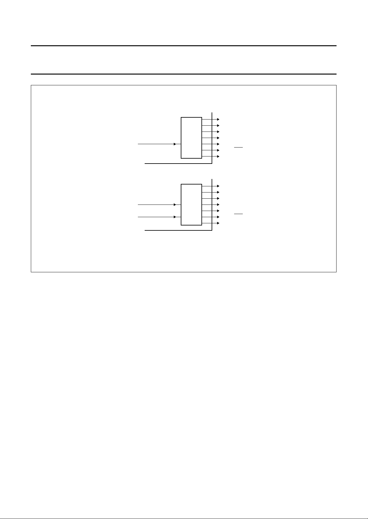
1 FEATURES
2 GENERAL DESCRIPTION
3 QUICK REFERENCE DATA
4 ORDERING INFORMATION
5 BLOCK DIAGRAM
6 PINNING
7 FUNCTIONAL DESCRIPTION
7.1 Functional overview
7.1.1 MPEG-2 syntax parser
7.1.2 Error handling
7.1.3 Teletext filter
7.1.4 Generic data filter
7.1.5 High speed data filter
7.1.6 Video data filter
7.1.7 Audio data filter
7.1.8 Program clock reference processor
7.1.9 Time stamp processors
7.1.10 FIFO buffers
7.1.11 Microcontroller interface
7.1.11.1 Short filters
7.1.11.2 Long filters
7.1.11.3 Subtitling filter
7.2 MPEG-2 systems parsing
7.3 Error handling
7.4 Interfacing to the external descrambler
7.5 High speed data interfacing
7.6 Interfacing to Philips SAA7201 video decoder
7.7 Interfacing to a third party video decoder
7.8 Interfacing to SAA2500 and third party audio
decoders
7.9 Interfacing to combined audio/video decoders
7.10 Interfacing to SAA9042 and SAA5270 teletext
decoders and SAA7183 EURO-DENC
7.11 Program clock reference processing
7.12 Time stamp processing (PTS/DTS)
7.13 Output buffering for audio and video
7.14 Microcontroller interfacing
7.14.1 Short filter module
7.14.2 Long filter module
7.14.3 Subtitling filter
8 PROGRAMMING THE DEMULTIPLEXER
9 LIMITING VALUES
10 HANDLING
11 DC CHARACTERISTICS
12 AC CHARACTERISTICS
13 APPENDIX
14 PACKAGE OUTLINE
15 SOLDERING
15.1 Introduction
15.2 Reflow soldering
15.3 Wave soldering
15.4 Repairing soldered joints
16 DEFINITIONS
17 LIFE SUPPORT APPLICATIONS
1997 Jan 21 2

Philips Semiconductors Preliminary specification
MPEG-2 systems demultiplexer SAA7205H
1 FEATURES
• Input data fully compliant with the Transport Stream
(TS) definition of the MPEG-2 systems specification
(International Standard; November 1994)
• Input data signals: Forward Error Correction (FEC) or
descrambler interface
– modem data input bus (8-bit wide)
PKTDAT7 to PKTDAT0
– valid input data indicator (PKTDATV)
– erroneous packet indicator (PKTBAD/PKTBAD)
– first packet byte indicator (PKTSYNC)
– byte strobe signal [for the asynchronous mode only
(PKTBCLK)]
• The interface can be configured to either of two modes:
– asynchronous mode; PKTBCLK < 9 MHz, for
connection to a modem (e.g. FEC)
– synchronous mode; PKTBCLK is not used for
connection to an external descrambler operating at
9 MHz. The descrambler chip clock (9 MHz; 33%
duty cycle) is generated and output to the
demultiplexer.
The descrambler chip clock [DCLK (9 MHz, 33% duty
cycle)] is generated and output by the demultiplexer
• External memory; standard 32K × 8-bit static RAM.
Required typical access time ≤ 50 ns, write pulse width
) ≤ 35 ns.
(t
WP
• Effective bit rate: f
• Control Interface; 8-bit multiplexed data/address
(MDAT7 to MDAT0), memory mapped I/O (P90CE201
microcontroller parallel bus compatible), in combination
with two microcontroller interrupt signals (IRQ andNMI).
In addition, a number of address input pins
(MA9 to MA2) allow direct access to a selected set of
demultiplexer registers.
• Output ports:
Video; two alternative applications;
– third party video decoder compatible (master or slave
horizontal or vertical sync generation)
– Philips SAA7201 compatible (via general purpose
output)
≤ 72 MHz
bit
Audio; third party audio decoder, or Philips SAA2500
compatible
Audio/video; third party combined A/V decoder
compatible, (programmable)
Teletext; a Teletext Clock/Teletext Data (TTC/TTD)
based serial interface to selected teletext decoders
(e.g. SAA9042). Alternatively, this interface can be
programmed to provide data for Vertical Blanking
Interval (VBI) insertion of teletext data. The interface
therefore includes a teletext data request input (TTR).
In this mode, the interface is compatible with the
SAA7183 (EURO-DENC) TXT interface.
HS Data; high-speed data output, outputting entire
transport packets, packet payloads, PES packet
payloads, or sections (programmable) at byte clock
frequency (9 MHz). In the test mode it is capable of
outputting copies of either video, audio or other data
streams (programmable).
HS pins are combined with the general purpose
interface. The general purpose interface is bidirectional,
and can therefore, be used as an alternative transport
stream input.
• Descrambler; 8-bit wide data input interface, combined
with the modem input bus. A descrambler device may
output a descrambled transport stream at 9 MByte/s.
A 9 MHz descrambler clock is generated and output by
the demultiplexer.
• Microcontroller support; only for control, no specific
demultiplexing tasks are performed by the
microcontroller. However, parsing and processing of
Program Specific Information (PSI), and Service
Information (SI) is left to the microcontroller.
• Error handling; stream dependent error handling
algorithms, invoked either if the
signal is set, or if the transport_error_indicator bit
(MPEG-2 syntax) is set or if the parser detects an
MPEG-2 syntax error. Different handling algorithms are
applied for the various output ports.
PKTBAD/PKTBAD input
1997 Jan 21 3
Philips Semiconductors Preliminary specification
MPEG-2 systems demultiplexer SAA7205H
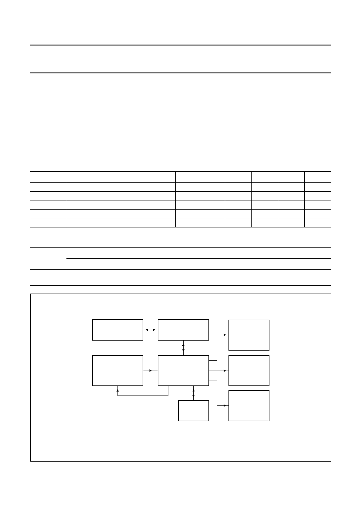
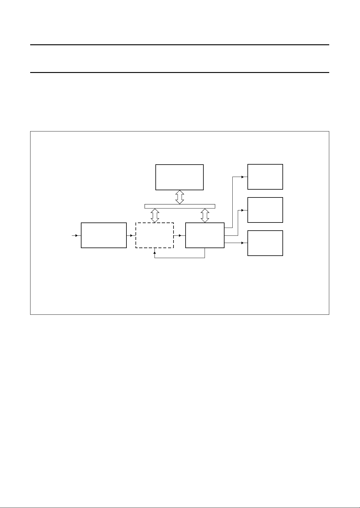
2 GENERAL DESCRIPTION
This document specifies the MPEG-2 systems demultiplexer IC, SAA7205H, for use in MPEG-2 based digital TV
receivers, possibly incorporating conditional access. Such receivers are to be implemented in, for instance, a Digital
Video Broadcasting (DVB) set-top box, or Integrated Receiver Decoder (IRD). An example of a
demultiplexer/descrambler system configuration, containing a channel decoder module, source decoders, a system
microcontroller and a conditional access system is shown in Fig.1. The main function of the demultiplexer is to separate
relevant data from an incoming MPEG-2 systems compliant data stream and pass it to both the individual source
decoders and to the system microcontroller. To support descrambling, the demultiplexer interfaces with the descrambler
part of a conditional access system (optional). The demultiplexer therefore generates a 9 MHz descrambler chip clock.
3 QUICK REFERENCE DATA
SYMBOL PARAMETER CONDITIONS MIN. TYP. MAX. UNIT
V
DDD
V
DDD(core)
P
tot
f
CLK
T
amb
digital supply voltage 4.5 5.0 5.5 V
digital supply voltage for core 3.0 3.3 3.6 V
total power consumption −−380 mW
clock frequency f
≤ 9 MHz −−27 MHz
byte
operating ambient temperature 0 − 70 °C
4 ORDERING INFORMATION
TYPE
NUMBER
NAME DESCRIPTION VERSION
PACKAGE
SAA7205H QFP128 plastic quad flat package; 128 leads (lead length 1.6 mm);
body 28 × 28 × 3.4 mm; high stand-off height
handbook, full pagewidth
CONDITIONAL
ACCESS
SYSTEM
DEMODULATOR PLUS
FORWARD ERROR
CORRECTOR
(AND DESCRAMBLER)
9 MHz DCLK
MICROCONTROLLER
SAA7205H
32K x 8
SRAM
DECODER
DECODER
TELETEXT
DECODER
SOT320-2
AUDIO
SOURCE
VIDEO
SOURCE
Fig.1 Demultiplexer system configuration.
1997 Jan 21 4
MGG374
Philips Semiconductors Preliminary specification
MPEG-2 systems demultiplexer SAA7205H
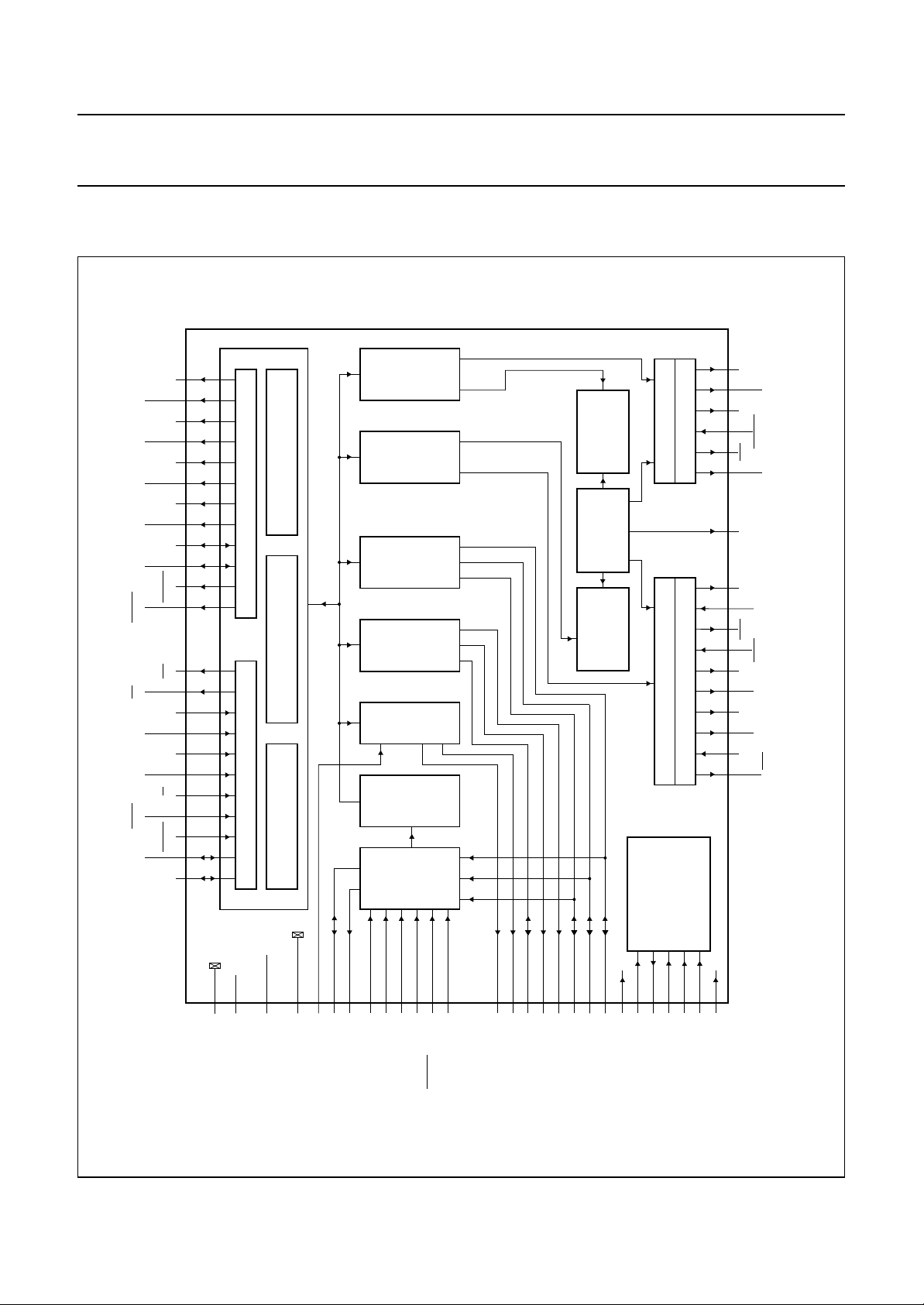
5 BLOCK DIAGRAM
MGG373
59
to
RAMA5
65,
RAMA8
75 71,
70
RAMA11
68
73
RAMA13
69
55
RAMIO0
74 49
WERAM
54
NMI
86 101 102
MA0
87
88
MA9
97
R/W
100 99 98
77
CSDEM
1
VO0
64
66
72
SUBTITLING/
PRIVATE FILTER
RAM INTERFACE
to
57
to
53
MODULE
LONG FILTER
to
95
DATA
AUDIO
FILTER
DATA
VIDEO
FILTER
DATA
FILTER
GENERIC
FILTER
H/S DATA
TXT
FILTER
DECODING
TIME STAMP
PROCESSOR
PRESENTATION/
REFERENCE
PROCESSOR
PROGRAM CLOCK
DECODING
TIME STAMP
PROCESSOR
PRESENTATION/
BUFFER
BUFFER
CONTROL
CONTROL
SAA7205H
ERROR
STREAM
TRANSPORT
HANDLING
AND
AF PARSER
FOR
TEST CONTROL BLOCK
BOUNDARY SCAN TEST
AND
SCAN TEST
MODULE
MICROCONTROLLER INTERFACE
to
84
to
8
SHORT FILTER
AUDAT
AUDATCLK
AUDATV
AUDATR
AUE
10 11 15 14 13 12
AUDECLK
33
COMSYNC PWMO
VSEL
CLKP
VREQ
CLK13.5
CbREF
HSYNC
VSYNC
VIN
40 47 42 43 45 46 128 127 104 44
EVEN/ODD
Fig.2 Block diagram.
to
RAMA0
RAMA7
RAMA6,
RAMA9,
RAMA10
RAMA12
RAMA14
to
RAMIO2
to
RAMIO3
RAMIO7
OERAM
handbook, full pagewidth
IRQ
MA1
to
MA2
MA10
CSVID
to
MDAT0
MDAT7
to
VO7
16, 85
SSD(core)
V
23, 76
9, 34, 41,
DDD(core)
V
32, 36, 48, 67,
105, 113, 126
58, 96, 120
DDD6
V
DDD1 to
V
37
SSD7
V
SSD1 to
V
24 to 31
TTR
109 to 112
118
119
DCLK
PKTBCLK
GPO7 to GPO0
114 to 117
PKTDAT7 to PKTDAT4
PKTDAT3 to PKTDAT0
107
108
106
PKTDATV
PKTSYNC
PKTBAD/PKTBAD
1997 Jan 21 5
38
39
TTD
TTC
171819
21
20
22
HSE
HSV
HSSYNC
GPV
GPST
35
CCLKI
GPSYNC
121
TC0/TDI
122
TDO
123
TMS
124
125
TRST
TC1/TCLK
103
POR

Philips Semiconductors Preliminary specification
MPEG-2 systems demultiplexer SAA7205H
6 PINNING
SYMBOL PIN I/O DESCRIPTION
VO7 1 I/O data output bit 7 to video decoder (shared with microcontroller data)
VO6 2 I/O data output bit 6 to video decoder (shared with microcontroller data)
VO5 3 I/O data output bit 5 to video decoder (shared with microcontroller data)
VO4 4 I/O data output bit 4 to video decoder (shared with microcontroller data)
VO3 5 I/O data output bit 3 to video decoder (shared with microcontroller data)
VO2 6 I/O data output bit 2 to video decoder (shared with microcontroller data)
VO1 7 I/O data output bit 1 to video decoder (shared with microcontroller data)
VO0 8 I/O data output bit 0 to video decoder (shared with microcontroller data)
V
DDD1
AUDECLK 10 O audio decoder clock output [equals CCLKI/M (programmable)]
AUE 11 O audio data error indicator output (active LOW)
AUDAT 12 O data output to audio decoder (elementary stream)
AUDATCLK 13 O audio data clock output (frequency range 32 to 448 kHz; 9 Mbit/s)
AUDATV 14 O audio data valid indicator output
AUDATR 15 I audio data request input (active LOW)
V
SSD1(core)
GPV 17 I/O valid data byte indicator input/output
GPST 18 I/O byte strobe signal input/output (equals 9 MHz gated byte clock)
GPSYNC 19 I/O packet sync byte indicator input/output
HSE 20 I/O indicates erroneous HS data input/output
HSV 21 O valid high speed data indicator
HSSYNC 22 O indicates the first output byte of either a packet or payload
V
DDD1(core)
GPO7 24 I/O high speed byte output bit 7 for transport packets/general purpose byte output
GPO6 25 I/O high speed byte output bit 6 for transport packets/general purpose byte output
GPO5 26 I/O high speed byte output bit 5 for transport packets/general purpose byte output
GPO4 27 I/O high speed byte output bit 4 for transport packets/general purpose byte output
GPO3 28 I/O high speed byte output bit 3 for transport packets/general purpose byte output
GPO2 29 I/O high speed byte output bit 2 for transport packets/general purpose byte output
GPO1 30 I/O high speed byte output bit 1 for transport packets/general purpose byte output
GPO0 31 I/O high speed byte output bit 0 for transport packets/general purpose byte output
V
SSD1
PWMO 33 O pulse width modulated VCO control signal output (local STC)
9 supply digital supply voltage 1 (+5 V)
16 GND digital ground 1 for core
23 supply digital supply voltage 1 for core (+3.3 V)
(e.g. for SAA7201)/alternative transport stream input
(e.g. for SAA7201)/alternative transport stream input
(e.g. for SAA7201)/alternative transport stream input
(e.g. for SAA7201)/alternative transport stream input
(e.g. for SAA7201)/alternative transport stream input
(e.g. for SAA7201)/alternative transport stream input
(e.g. for SAA7201)/alternative transport stream input
(e.g. for SAA7201)/alternative transport stream input
32 GND digital ground 1
1997 Jan 21 6

Philips Semiconductors Preliminary specification
MPEG-2 systems demultiplexer SAA7205H
SYMBOL PIN I/O DESCRIPTION
V
DDD2
CCLKI 35 I 27 MHz demultiplexer chip clock Input
V
SSD2
TTR 37 I teletext data request input (for VBI insertion of TXT)
TTD 38 O serial teletext data output (6.75 or 6.9375 Mbit/s)
TTC 39 O TXT clock (6.75 MHz = CCLKI/4)
ODD 40 O field parity output, internally generated, locked to COMSYNC
EVEN/
V
DDD3
VSYNC 42 O vertical sync output, locked to CCLKI and optionally VIN
HSYNC 43 O horizontal sync output, internally generated
COMSYNC 44 O (CCIR601) composite sync (50 and 60 Hz)
CbREF 45 O indicating U samples in UY and VY video decoder output
CLK13.5 46 O equals CCLKI/2
VIN 47 I receiver local vertical sync input, locked to CCLKI (optional)
V
SSD3
RAMIO3 49 I/O external SRAM input/output bus bit 3
RAMIO4 50 I/O external SRAM input/output bus bit 4
RAMIO5 51 I/O external SRAM input/output bus bit 5
RAMIO6 52 I/O external SRAM input/output bus bit 6
RAMIO7 53 I/O external SRAM input/output bus bit 7
OERAM 54 O output enable for external 32K × 8 SRAM (active LOW)
RAMIO2 55 I/O external SRAM input/output bus bit 2
RAMIO1 56 I/O external SRAM input/output bus bit 1
RAMIO0 57 I/O external SRAM input/output bus bit 0
V
DDD4
RAMA0 59 O external SRAM address bus output bit 0
RAMA1 60 O external SRAM address bus output bit 1
RAMA2 61 O external SRAM address bus output bit 2
RAMA3 62 O external SRAM address bus output bit 3
RAMA4 63 O external SRAM address bus output bit 4
RAMA5 64 O external SRAM address bus output bit 5
RAMA6 65 O external SRAM address bus output bit 6
RAMA7 66 O external SRAM address bus output bit 7
V
SSD4
RAMA12 68 O external SRAM address bus output bit 12
RAMA14 69 O external SRAM address bus output bit 14
RAMA11 70 O external SRAM address bus output bit 11
RAMA9 71 O external SRAM address bus output bit 9
RAMA8 72 O external SRAM address bus output bit 8
RAMA13 73 O external SRAM address bus output bit 13
WERAM 74 O write enable output for external SRAM (active LOW)
34 supply digital supply voltage 2 (+5 V)
36 GND digital ground 2
41 supply digital supply voltage 3 (+5 V)
48 GND digital ground 3
58 supply digital supply voltage 4 (+5 V)
67 GND digital ground 4
1997 Jan 21 7

Philips Semiconductors Preliminary specification
MPEG-2 systems demultiplexer SAA7205H
SYMBOL PIN I/O DESCRIPTION
RAMA10 75 O external SRAM address bus output bit 10
V
DDD2(core)
MDAT0 77 I/O microcontroller bidirectional data bus bit 0
MDAT1 78 I/O microcontroller bidirectional data bus bit 1
MDAT2 79 I/O microcontroller bidirectional data bus bit 2
MDAT3 80 I/O microcontroller bidirectional data bus bit 3
MDAT4 81 I/O microcontroller bidirectional data bus bit 4
MDAT5 82 I/O microcontroller bidirectional data bus bit 5
MDAT6 83 I/O microcontroller bidirectional data bus bit 6
MDAT7 84 I/O microcontroller bidirectional data bus bit 7
V
SSD2(core)
MA0 86 I microcontroller MSByte/
MA1 87 I microcontroller address/
MA2 88 I microcontroller address input bit 2 for direct access to selected registers
MA3 89 I microcontroller address input bit 3 for direct access to selected registers
MA4 90 I microcontroller address input bit 4 for direct access to selected registers
MA5 91 I microcontroller address input bit 5 for direct access to selected registers
MA6 92 I microcontroller address input bit 6 for direct access to selected registers
MA7 93 I microcontroller address input bit 7 for direct access to selected registers
MA8 94 I microcontroller address input bit 8 for direct access to selected registers
MA9 95 I microcontroller address input bit 9 for direct access to selected registers
V
DDD5
MA10 97 I microcontroller direct addressing/indirect addressing indicator input bit 10
W 98 I read/write input selection
R/
CSVID 99 I (audio)/video decoder chip select input (active LOW)
CSDEM 100 I demultiplexer chip select input (active LOW)
IRQ 101 O interrupt request output for microcontroller (active LOW, open-drain)
NMI 102 O non-maskable interrupt output for VOUT bus access handling (open-drain)
POR 103 I power-on reset input
VSEL 104 I video input select signal (bus control by microcontroller)
V
SSD5
PKTSYNC 106 I indicates the first input byte (sync) of a transport packet
PKTDATV 107 I valid input data indicator
PKTBAD/
PKTBAD
PKTDAT7 109 I 8-bit wide modem data input bit 7
PKTDAT6 110 I 8-bit wide modem data input bit 6
PKTDAT5 111 I 8-bit wide modem data input bit 5
PKTDAT4 112 I 8-bit wide modem data input bit 4
V
SSD6
PKTDAT3 114 I 8-bit wide modem data input bit 3
76 supply digital supply voltage 2 for core (+3.3 V)
85 GND digital ground 2 for core
LSByte indicator input bit 0
data indicator input bit 1
96 supply digital supply voltage 5 (+5 V)
105 GND digital ground 5
108 I packet error indicator input (programmable polarity)
113 GND digital ground 6
1997 Jan 21 8

Philips Semiconductors Preliminary specification
MPEG-2 systems demultiplexer SAA7205H
SYMBOL PIN I/O DESCRIPTION
PKTDAT2 115 I 8-bit wide modem data input bit 2
PKTDAT1 116 I 8-bit wide modem data input bit 1
PKTDAT0 117 I 8-bit wide modem data input bit 0
PKTBCLK 118 I byte strobe input signal (< 9 MHz)
DCLK 119 O 9 MHz descrambler chip clock output (33% duty cycle)
V
DDD6
TC0/TDI 121 I scan test data input/boundary scan test data input
TDO 122 O boundary scan test data output
TMS 123 I boundary scan test input mode select
TC1/TCLK 124 I scan test clock input/ boundary scan test clock input
TRST 125 I boundary scan test reset input (LOW in normal operation)
V
SSD7
CLKP 127 O gated clock output signal indicating valid data (9 MHz = CCLKI/3; active LOW)
VREQ 128 I video data request input (active LOW)
120 supply digital supply voltage 6 (+5 V)
126 GND digital ground 7
1997 Jan 21 9
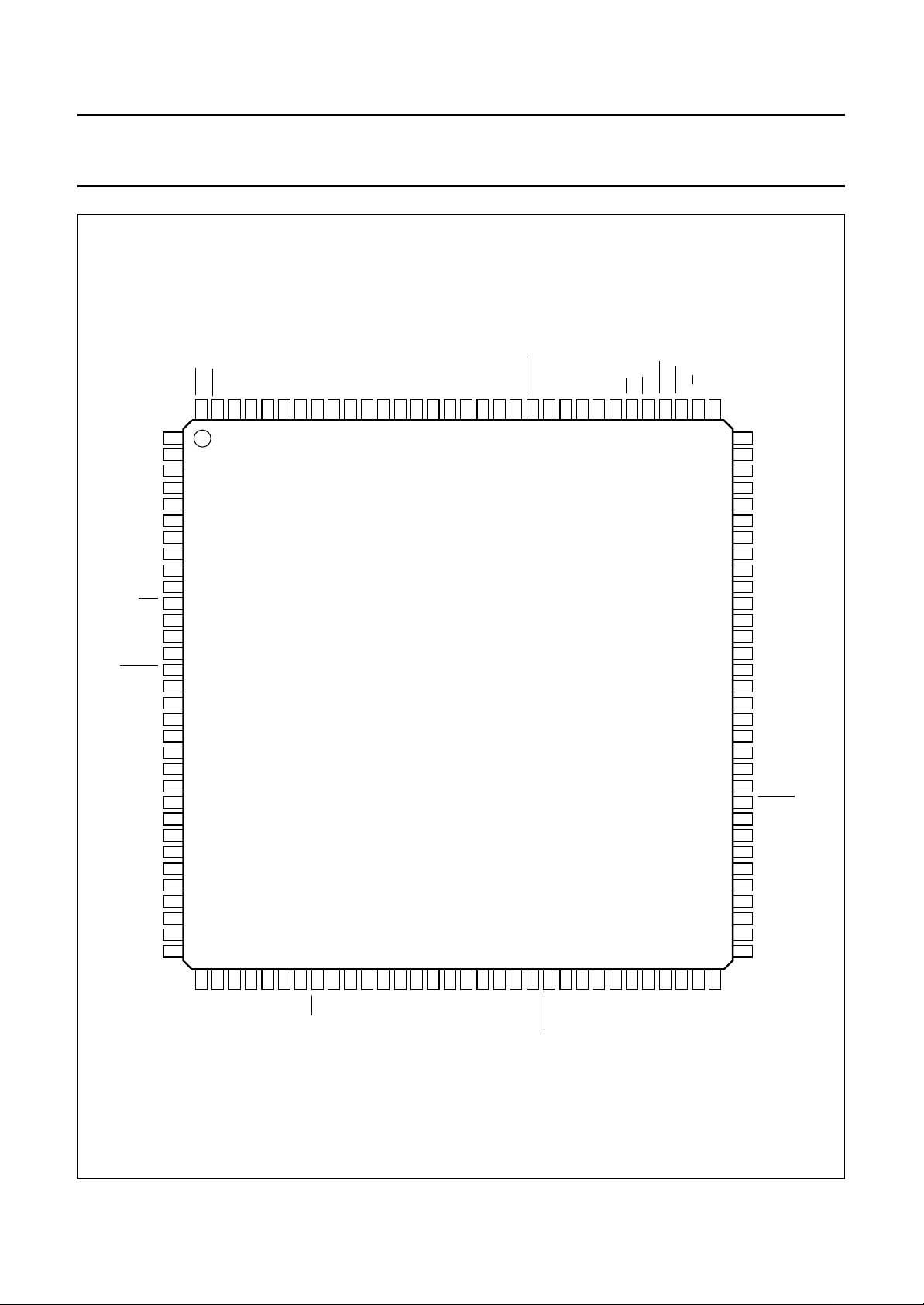
Philips Semiconductors Preliminary specification
MPEG-2 systems demultiplexer SAA7205H
handbook, full pagewidth
VO7
1
VO6
2
3
VO5
4
VO4
5
VO3
6
VO2
7
VO1
VO0
8
V
9
DDD1
AUE
AUDAT
AUDATV
AUDATR
GPV
GPST
HSE
HSV
GPO7
GPO6
GPO5
GPO4
GPO3
GPO2
GPO1
GPO0
V
SSD1
10
11
12
13
14
15
16
17
18
19
20
21
22
23
24
25
26
27
28
29
30
31
32
AUDECLK
AUDATCLK
V
SSD1(core)
GPSYNC
HSSYNC
V
DDD1(core)
VREQ
128
CLKP
127
SSD7
V
126
TRST
125
TC1/TCLK
TMS
TDO
122
124
123
DDD6
TC0/TDI
V
121
120
DCLK
119
PKTBCLK
PKTDAT0
118
117
PKTDAT1
116
PKTDAT2
115
SSD6
PKTDAT3
V
PKTDAT4
114
112
113
SAA7205H
PKTDAT5
111
PKTDAT6
PKTDAT7
PKTBAD/PKTBAD
110
109
108
PKTDATV
PKTSYNC
107
106
SSD5
V
105
VSEL
104
POR
103
NMI
102
IRQ
101
CSDEM
CSVID
999897
100
R/W
MA10
96
95
94
93
92
91
90
89
88
87
86
85
84
83
82
81
80
79
78
77
76
75
74
73
72
71
70
69
68
67
66
65
V
DDD5
MA9
MA8
MA7
MA6
MA5
MA4
MA3
MA2
MA1
MA0
V
SSD2(core)
MDAT7
MDAT6
MDAT5
MDAT4
MDAT3
MDAT2
MDAT1
MDAT0
V
DDD2(core)
RAMA10
WERAM
RAMA13
RAMA8
RAMA9
RAMA11
RAMA14
RAMA12
V
SSD4
RAMA7
RAMA6
3334353637
SSD2
DDD2
CCLKI
PWMO
V
V
39404142434445464748495051525354555657585960616263
38
TTR
TTD
TTC
EVEN/ODD
DDD3
V
VSYNC
HSYNC
COMSYNC
CbREF
CLK13.5
VIN
SSD3
V
Fig.3 Pin configuration.
1997 Jan 21 10
RAMIO3
RAMIO4
RAMIO5
RAMIO6
OERAM
RAMIO7
RAMIO2
RAMIO1
DDD4
V
RAMIO0
RAMA0
RAMA1
RAMA2
RAMA3
64
RAMA4
RAMA5
MGG372

Philips Semiconductors Preliminary specification
MPEG-2 systems demultiplexer SAA7205H
7 FUNCTIONAL DESCRIPTION
7.1 Functional overview
A schematic diagram of the internal structure of the
MPEG-2 demultiplexer is shown in Fig.2. The diagram
illustrates the main functional entities in the demultiplexer.
7.1.1 MPEG-2
SYNTAX PARSER
The MPEG-2 syntax parser, parsing transport streams
which comply with the MPEG-2 systems specification
(International Standard, November 1994).
7.1.2 E
RROR HANDLING
Error handling is invoked whenever an error is detected.
Error handling is started on the basis of either the
PKTBAD/PKTBAD input signal (driven by the FEC
decoder), or the transport_error_indicator in the transport
packet header, or discovery of a syntax error by the parser.
7.1.3 T
ELETEXT FILTER
A teletext (TXT) filter, generating a teletext clock
(TTC = 6.75 MHz, derived from the chip clock,
CCLKI = 27 MHz) and providing a serial TXT data stream
(TTD) locked to both TTC and the horizontal video sync
(HSYNC) generated by the demultiplexer. In accordance
with the DVB specification, TXT data is transported in
MPEG-2 PES packets. The incoming transport stream is
filtered on the basis of a Programmable Packet
Identification (PID) and elementary stream data is stored
in a 2 kbyte FIFO buffer. Data is read from the TXT buffer
at 6.75 Mbit/s.
The TXT filter can, alternatively, be programmed to a
mode in which it provides TXT bits at 6.9375 MHz, on the
basis of an external request (TTR). This mode is applied
for vertical blanking interval insertion of TXT data. It is
compatible with the TXT input of the EURO-DENC
(SAA7183).
7.1.4 G
ENERIC DATA FILTER
A generic data filter is connected to the generic interface.
This filter in fact does not filter, but passes the entire
transport stream in byte format. A byte strobe signal
(GPST), indicating consecutive valid bytes, a valid signal
(GPV) and a header sync byte indicator (GPSYNC) are
generated.
Alternatively the general purpose interface can be
configured to function as transport stream input
(GP_Direction = 1; address 0x0700; see Table 13).
7.1.5 H
IGH SPEED DATA FILTER
A high speed data filter (HS), retrieves the entire transport
packets, packet payloads, PES payloads or sections from
the input stream on the basis of a programmable filter.
Data is output at the byte clock frequency
(DCLK = 9 MHz = CCLKI/3, 33% duty cycle). Selected
parts of a data stream are indicated by the HSV signal.
The first byte of a data entity is indicated by HSSYNC. The
HS filter shares its data output pins with the generic data
filter.
It should be noted that in the event that the HS filter is
programmed to the section mode, the GP bus only outputs
selected sections and not an entire transport stream.
7.1.6 V
IDEO DATA FILTER
A video data filter, with a decoder specific interface. This
filter selects either Packetized Elementary Stream (PES)
data, or Elementary Stream (ES) data (programmable) on
the basis of a programmable PID, and passes it to the
video FIFO. Presentation Time Stamps and Decoding
Time Stamps (PTS and DTS) are obtained from the PES
stream and can be read by the microcontroller (optional).
Video PES or ES data is output at 9 MHz, via a
bidirectional 8-bit wide bus which is time-shared with the
microcontroller. Access to the output bus is controlled by
the microcontroller using the VSEL signal.
The demultiplexer therefore, halts output video data
whenever VSEL = 0 and creates a bidirectional
communication link between the microcontroller and the
video decoder.
7.1.7 A
UDIO DATA FILTER
An audio data filter with a decoder specific interface. This
filter selects PES or ES data (programmable) on the basis
of a programmable PID and passes it to the audio FIFO.
Time-stamps are retrieved from audio PES headers and
can be read by the microcontroller (optional).
The audio filter can be switched to a mode in which the
microcontroller controls audio and video synchronization
(software sync). In this mode the filter outputs audio data
at 9 Mbit/s. The filter is also capable of handling
synchronization independently from the microcontroller.
In this situation the audio elementary stream output is
(hardware) synchronized to the System Time Clock (STC)
automatically. In the hardware synchronization mode, the
audio elementary stream data is output via a bit serial data
link at a bit rate between 32 to 448 kbit/s. The actual bit
rate depends on the type of audio frame that is handled
(as specified in the MPEG-2 audio specification).
1997 Jan 21 11

Philips Semiconductors Preliminary specification
MPEG-2 systems demultiplexer SAA7205H
It should be noted that audio and video data can be
optionally combined on the output bus to interface to
combined audio/video decoders. In this mode the video
bus is controlled by the VSEL signal, an audio request
signal (AUDATR) and a video request signal (VREQ;
optional). Video and audio bytes are output at 9 MBytes
and are interleaved with a programmable audio/video
ratio.
7.1.8 P
ROGRAM CLOCK REFERENCE PROCESSOR
The PCR processor is capable of regenerating a local
system time clock. This block contains a digital clock
recovery loop. Two local clock counters generate an
absolute timing value (cycle time approximately 24 hours),
which is used to verify the phase relationship between the
local system time clock and the transmitter reference clock
(Program Clock Reference, or PCR). Two STC counters
are implemented to allow for correct handling of PCR
discontinuations.
7.1.9 T
IME STAMP PROCESSORS
These two PTS/DTS processors are capable of
synchronizing attached source decoders. The PTS/DTS
processors retrieve time stamps from the incoming
transport stream. They also compare emulated time
stamps (PTS/DTS) with the local absolute time value
generated by the PCR processor. In the event of equality
a microcontroller interrupt is generated.
The microcontroller can respond to this pulse by
instructing the attached source decoders to start decoding,
or to start presentation. For audio, the PTS values are
stored in the audio FIFO to be used for synchronization of
the FIFO output stream (called lip-sync).
7.1.10 FIFO
BUFFERS
There are two FIFO buffers for audio and video (6 kBytes
and 768 Bytes respectively), including buffer control, to
interface between different clock systems. These FIFOs
are filled at byte clock (CCLKI/3) frequency and emptied
on the acquisition clocks of the respective source
decoders [9 MByte/s for video and combined audio/video,
and a frequency in the range 32 to 448 kbit/s (hardware
sync), or 9 Mbit/s (software sync) for audio].
7.1.11 M
ICROCONTROLLER INTERFACE
The microcontroller interface provides protocol handling
for the memory mapped I/O control bus (Philips
P90CE201 compatible). This module also contains an
interrupt request handler and data filters for retrieval of
Program Specific Information (PSI), service information
(SI), Electronic Program Guides (EPG) (private sections),
subtitling (private sections) and low speed (LS) data
(private).
7.1.11.1 Short filters
The short filters select data on the basis of PIDs and a
combination of MPEG-2 section addressing fields.
Selected data is stored in twelve 1 kByte (constrained
random access) buffers. These buffers are located in the
external SRAM memory and can be read by the
microcontroller. The short filters are capable of monitoring
12 section streams simultaneously.
7.1.11.2 Long filters
The long filters also select data on the basis of PIDs and a
combination of MPEG-2 section addressing fields.
Selected data is stored in four 4 kByte (constrained
random access) buffers. These buffers are located in the
external SRAM memory and can be read by the
microcontroller. The long filters are capable of monitoring
4 section streams simultaneously.
7.1.11.3 Subtitling filter
The subtitling filter is capable of retrieving transport packet
payloads or PES payloads from the input stream, on the
basis of a programmable filter. It is also capable of
retrieving adaptation field and PES header private data.
Data is stored in a 4 kByte FIFO which is located in the
external SRAM memory and can be read by the
microcontroller.
Table 1 Filter types
FILTER TYPE NUMBER OF FILTERS BUFFER SIZE REMARKS
Short (sections) 12 12 × 1 kByte −
Long (sections) 4 4 × 4 kByte −
Subtitling 1 1 × 4 kByte PES and PES payload (ES), adaption field
private data, PES header private data
1997 Jan 21 12

Philips Semiconductors Preliminary specification
MPEG-2 systems demultiplexer SAA7205H
7.2 MPEG-2 systems parsing
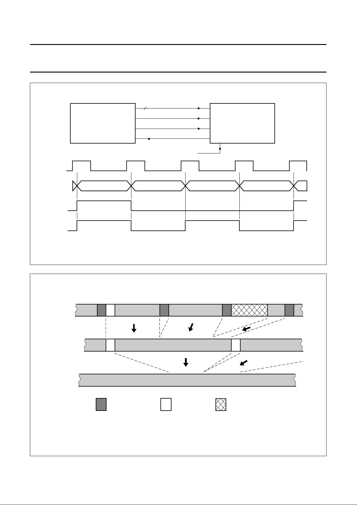
The demultiplexer receives data from a Forward Error
Correction (FEC) decoder (see Fig.4) or a descrambler
(see Fig.5) in a digital TV receiver in the following input
data format:
• A number of data bits via PKTDAT7 to PKTDAT0
(8-bit wide input bus)
• A valid input data indicator signal (PKTDATV) which is
HIGH for consecutive valid bytes and output by either a
FEC decoder or a descrambler. The demultiplexer input
is allowed to have a ‘bursty’ nature.
• A transport packet error indicator (
which is HIGH for the duration of each 188 byte
transport packet in which the FEC decoder found more
errors than it could correct. The polarity (active HIGH or
LOW) of the error indicator is programmable
(bit Bad_polarity, address 0x0100; see Table 13).
• A packet sync signal (PKTSYNC) which goes HIGH at
the start of the first byte of a transport packet. Only the
rising edge of PKTSYNC is used for synchronization,
the exact HIGH time of the signal is therefore irrelevant.
• A byte strobe signal [PKTBCLK (< 9 MHz)] which
indicates consecutive data bytes in the input stream, in
the non-9 MHz mode only (bit 9 MHz_interface = 0,
address 0x0100;see Table 13). PKTBCLK is used as an
enable signal and transport stream input bytes are
sampled on its rising edges of the clock pulse. If the
input interface is programmed to the 9 MHz mode
(9 MHz interface = 1), the PKTBCLK signal is ignored.
• A descrambler clock signal [DCLK (9 MHz, 30% duty
cycle)] which is the data output clock for the
descrambler. If rising edges of this clock signal are used
to input data to the demultiplexer the 9 MHz mode must
be used (bit 9 MHz_interface = 1, address 0x0100;
see Table 13).
The parser module in the demultiplexer parses MPEG-2
systems compliant transport streams. MPEG-2 systems
specifies a hierarchical two level multiplex (see Fig.6).
The top hierarchical level is the transport stream,
consisting of relatively short (188 byte) transport packets.
Each transport packet consists of a 4 byte transport
header, an optional adaptation field and a payload.
PKTBAD/PKTBAD)
The transport header contains a 13-bit packet
identification field. The adaptation field may contain
Program Clock Reference (PCR) data and transport
private data, among others. Both the transport header and
the optional adaptation fields are parsed by the parser
module within the demultiplexer. The individual states of
the MPEG-2 parser in the demultiplexer are listed in
Table 14.
The hierarchical multiplex level below the MPEG-2
transport stream and the packetized elementary stream, is
partly parsed by the demultiplexer, for instance in the
audio and video filters. A packetized elementary stream
consists of an elementary stream (e.g. MPEG-2 audio, or
video data) which is divided into subsequent variable
section lengths. To each section a PES header is added,
thus creating PES packets. A PES header may contain
time stamp information (PTS or DTS), scrambling control,
copy information and PES private data.
In the demultiplexer, parsing is performed for all incoming
transport packets. The parser is synchronized to a rising
edge on the PKTSYNC input. A microcontroller can
compose a set of PIDs by programming the appropriate
registers in the various filters within the demultiplexer. If a
packet is part of an audio or video transport stream, some
of the information fields in the transport and PES packet
headers are automatically retrieved. The microcontroller
can read the obtained information. Table 2 lists data that
can be accessed by the microcontroller, for both video
(address 0x0509; see Table 13) and audio streams
(address 0x0609; see Table 13).
MPEG-2 multiplex fields which are related to program
specific information (PSI), service information (SI), private
data and conditional access data (called sections) are
parsed partly in the section data filters. Program
association tables, program map tables and conditional
access tables can be retrieved from the stream and stored
in buffers in an external 32K × 8 SRAM. The same can be
performed (optional) for transport_private_data,
PES_private_data, and private sections in the subtitling
and section data filters. A microcontroller may access data
in the section data and subtitling buffers for further
processing in software.
1997 Jan 21 13
Philips Semiconductors Preliminary specification
MPEG-2 systems demultiplexer SAA7205H
Table 2 Microcontroller accessible MPEG-2 systems information
POSITION NUMBER OF BITS FIELD NAME FUNCTION
Transport packet
header
PES header 2 PES_scrambling_control
2 transport_scrambling_control
(bits: ts_scr_ctrl1 and 0)
indicates whether the associated bit
stream is scrambled or not
indicates whether the associated
(bits: pes_scr_ctrl1 and 0)
PES payload is scrambled or not
1 copyright (bit: cp_info1) anticopy management
1 original_or_copy (bit: cp_info0) anticopy management
1 additional_copy_info_flag
anticopy management
(bit: ad_cp_flag)
7 additional_copy_info
anticopy management
(bits: ad_cp_info7 to 0)
handbook, full pagewidth
PKTBCLK
PKTDAT7
PKTDAT0
PKTSYNC
PKTDATV
PKTBAD/PKTBAD
PKTBAD/PKTBAD
8
PKTDAT7 to PKTDAT0
FORWARD
ERROR
CORRECTOR
to
message invalid data
error-free transport packet (programmable polarity)
PKTBCLK
PKTDATV
PKTBAD/PKTBAD
PKTSYNC
erroneous transport packet
DEMULTIPLEXER
CCLKI
message invalid data
MGG375
Fig.4 Signal constellation FEC decoder - demultiplexer interfacing.
1997 Jan 21 14
Philips Semiconductors Preliminary specification
MPEG-2 systems demultiplexer SAA7205H
8
handbook, full pagewidth
DESCRAMBLER
DCLK
PKTDAT7 to PKTDAT0
PKTDATV
PKTSYNC
DCLK
DEMULTIPLEXER
CCLKI
PKTDAT7
to
PKTDAT0
PKTSYNC
PKTDATV
handbook, full pagewidth
transport
stream
packetized
elementary
stream
message invalid data
message
Fig.5 Signal constellation descrambler - demultiplexer interfacing.
invalid data
MGG376
elementary
stream
= transport_header = pes_header = stuffing
Fig.6 MPEG-2 two level hierarchical demultiplexing.
1997 Jan 21 15
MGG318

Philips Semiconductors Preliminary specification
MPEG-2 systems demultiplexer SAA7205H
7.3 Error handling
The error handling module responds to four situations in
which errors are present in the incoming stream:
• An erroneous packet is signalled to the demultiplexer,
by means of the PKTBAD/PKTBAD input signal.
The FEC decoder drives this signal LOW (or HIGH)
should it discovers that the number of errors in a packet
exceeds its correction capability. The polarity of the
PKTBAD/PKTBAD input signal is programmable
(bit Bad_pol, address 0x0100; see Table 13).
• The transport_error_indicator bit in the transport packet
header is set (equals logic 1), indicating that an error
occurred prior to, or during transmission
• A continuity counter discontinuity is detected
• The parser detects a syntax error in a packet, or is out
of sync.
In the first two cases, the transport_error_indicator bit in
the transport packet header is set. In all cases error
handling depends on the data stream the packet belongs
to, as indicated in Table 3. Most of the functions in this
table are executed in the data filters, not in the error
handling module. Error handling is therefore implemented
as a distributed function.
If the parser detects a syntax error or is out of sync, the
error handling module discards all incoming data, and an
interrupt is set (bit prs_sync_lost, address 0x0000,
see Table 13).
The error handling module keeps track of an average error
count. The module counts every occurrence of both
PKTBAD = 0 (or PKTBAD = 1) and
“transport_error_indicator = 1. The 16-bit error count value
can be read by the microcontroller, which can also reset
the counter every once in a while by writing all zeroes
(00..00) to the register (word cnt15 to cnt0], address
0x0200; see Table 13). The microcontroller can thus
determine an average packet error rate.
Table 3 Error handling algorithms
DATA STREAM OPTION ERROR HANDLING
Video third party decoder erroneous transport packets are discarded, no error flag is set, but a
sequence_error_code (0x000001B4) is inserted, whenever a
continuity_counter discontinuity is discovered
SAA7201 handling is altogether done in the SAA7201 source decoder
Audio − discard erroneous packets
TXT − discard erroneous packets
Subtitling − PES packet data are passed to the microcontroller. The error handling
decision is left to the microcontroller.
High speed
data
Section data − CRC calculation is performed in the filters. If an error is detected, an error flag
− programmable error handling (see Section “High speed data interfacing”)
(bit err_stat, address 0x0305 to 0x0314, see Table 13) is set. The error
handling decision is left to the microcontroller.
1997 Jan 21 16
Philips Semiconductors Preliminary specification
MPEG-2 systems demultiplexer SAA7205H
7.4 Interfacing to the external descrambler
An optional external descrambler can be incorporated in a digital TV receiver in the configuration indicated in Fig.7.
In such a configuration the demultiplexer generates a 9 MHz, 33% duty cycle descrambler clock (DCLK) signal
(see Fig.5). A descrambler could use this clock signal for data processing and outputting data. In such a configuration
the demultiplexer input interface is set to 9 MHz mode (bit 9 MHz_interface = 1, address 0x0100, see Table 13).
handbook, full pagewidth
SYSTEM
MICROCONTROLLER
VIDEO
DECODER
AUDIO
DECODER
DEMODULATOR
AND
FORWARD ERROR
CORRECTOR
OPTIONAL
DESCRAMBLER
DCLK (9 MHz)
MPEG2
DEMULTIPLEXER
SAA7205H
Fig.7 Digital TV receiver configuration including a descrambler.
TELETEXT
AND
H/S DATA
APPLICATIONS
MGG767
1997 Jan 21 17

Philips Semiconductors Preliminary specification
MPEG-2 systems demultiplexer SAA7205H
7.5 High speed data interfacing
The High Speed (HS) data filter module retrieves entire
transport packets, packet payloads, PES payloads, or
sections from the input stream, on the basis of a
programmable filter. The packets may contain data for
specific high speed data applications. In test mode
however, by reprogramming the filter
(word HS_pid12 to HS_pid0, address 0x0700;
see Table 13), data of other filters can be output. This
enables the user to monitor data streams directed to audio,
video, section data, and other filters. The HS data filter
features a programmable error handling mechanism. If the
‘HS_err_rmv’ (address 0x0701;see Table 13) bit is set,
erroneous output packets are removed from the stream.
If ‘HS_dupl_rmv’ (address 0x0701, see Table 13) is set,
the same is true for duplicate packets. Both removal
options can also be disabled.
In the single PID mode, the HS filter can be programmed
to operate in one of four filter modes (bits HS_mode,
address 0x0700, see Table 13), as indicated in Table 4.
Table 4 HS programmable filtering modes
OPERATING
MODE
Single PID
mode
Single PID
mode
(continued)
Multiple PID
mode
‘1 1..11’, indicating all PID
bits are relevant,
therefore only one
particular PID matches
‘1 1..11’, indicating all PID
bits are relevant,
therefore only one
particular PID matches
‘..0..1..’, indicating one or
more PID bits are don’t
care, so multiple PIDs
may match
PID MASK
(ADDRESS 0X0701;
see Table 13
FILTERING
OPTION
total TS packet outputs entire transport packets.
TS packet
payload
PES packet
payload
section outputs entire sections, based on
total TS packet output packet payloads only.
In multiple PID mode, only entire transport packets can be
output, for packets matching the PID specification.
Selected stream data is output (unbuffered) via the
GPO7 to GPO0 bus, at byte clock (DCLK) frequency
(rate = 9 MByte/s). Data is output in the format indicated in
Fig.8. The DCLK signal is a continuous byte clock.
The HSV signal is set for matching data only, otherwise it
is kept low. The HSSYNC signal indicates the position of
the first byte of the selected data, as indicated in Table 4.
Erroneous data is signalled by means of the HSE signal,
which is high for the duration of the erroneous packet.
In section mode HS data is selected on the basis of
table_id, and two section header bytes following the
section_length indicator (see Fig.26). For this purpose,
programmable filter masks are provided (address
0x0702 to 0x0704, see Table 13). If section mode is
selected, the general purpose output GPO7 to GPO0 does
not carry the full transport stream. Only selected sections
are output
FUNCTION HSSYNC
first byte of transport
(HS_mode = 00,
address 0x0700, see Table 13)
outputs transport packet
payloads for a selected PID.
(HS_mode = 01)
output PES packet payloads for a
selected PID. (HS_mode = 10)
PID, and table_id + 2 bytes
selection (addresses 0x0702 to
0x0704, see Table 13).
(HS_mode = 11 and
HS_sect_flt_en = 1)
(HS_mode = 00)
packet
first byte of transport
packet payload, only
if payload_unit_
start_indicator is set
first byte of PES
packet payload
first byte of section
header
first byte of transport
packet
1997 Jan 21 18
Philips Semiconductors Preliminary specification
MPEG-2 systems demultiplexer SAA7205H
handbook, full pagewidth
DMUX
GPO7 to GPO0
8
HSV
DCLK
HSE
HSSYNC
PID matched data non-matching PID
1 byte 1 byte
Fig.8 High speed data output format.
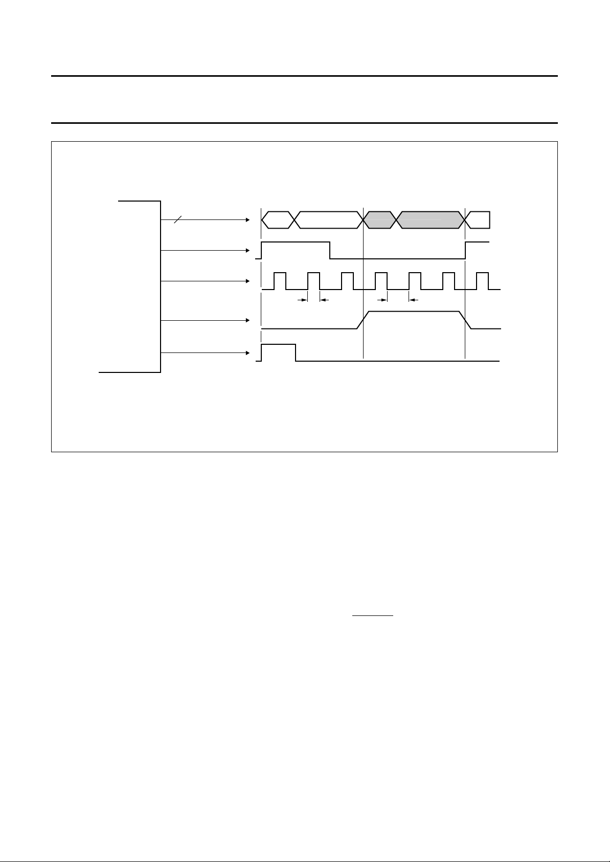
7.6 Interfacing to Philips SAA7201 video decoder
The Generic Data Filter (GDF) is connected to the General
Purpose interface, which shares its output bus
GPO7 to GPO0 with the high speed data interface.
This output can be used to interface with the Philips
SAA7201 video decoder. The GDF does not filter at all, it
merely passes the entire transport stream to the output in
byte format. The filter generates a GPST signal, which is a
gated byte clock, defined by a fixed high time (t
a minimum low time (t
) (see Fig.9). In addition to the
CLKOL
CLKOH
) and
strobe signal, the filter generates a GPV signal which can
be used in combination with the continuous DCLK to select
valid bytes, should a continuous clock be needed.
The filter furthermore generates a packet sync byte
indicator (GPSYNC).
1 byte 1 byte
t
t
CLKOH
CLKOL
MGG769
The general purpose interface is bidirectional and can
therefore serve as an alternative transport stream input to
the demultiplexer. The mode of the general purpose
interface is set by configuring the ‘GP_direction’ bit
(input = 1, output = 0, address 0x0700, see Table 13).
The GP pins have the following meaning when configured
to operate as inputs:
GPO7 to GPO0 = PKTDAT7 to PKTDAT0
GPST = PKTBCLK
GPSYNC = PKTSYNC
GPV = PKTDATV
HSE =
PKTBAD.
It should be noted that the HS filter is programmed to
section mode (see Table 4), the general purpose output is
not available.
1997 Jan 21 19

Philips Semiconductors Preliminary specification
MPEG-2 systems demultiplexer SAA7205H
handbook, full pagewidth
GPO7 to GPO0 byte 187 sync byte (0)
GPST
GPSYNC
GPV
consecutive transport packet bytes
t
CLKOH
Fig.9 Signal constellation for general purpose interface (SAA7201 compatible).
7.7 Interfacing to a third party video decoder
Communication to a third party video decoder involves
merging both video packetized elementary stream (PES)
or elementary stream (ES) data and control data on the
same 8-bit bidirectional bus VO7 to VO0 (see Fig.10).
PES or ES (bit: ‘video_pes_esn’, address 0x050A, see
Table 13) data is filtered by the video data filter and is
passed to a 768 Byte video FIFO buffer (see Section
“Output buffering for audio and video”), in which it is stored
at byte clock frequency (9 MHz). The video PES or ES
stream is read from the FIFO at video data acquisition
clock frequency
CLKP (equals 9 MHz = CCLKI/3, 67%
duty cycle, see Fig.10). However, CLKP is a gated clock
signal, which is frozen to logic 1 in case of control
exchange between the microcontroller and the video
decoder (⇒ VSEL = 0), or FIFO underflow (see Fig.10).
A bidirectional bus multiplexer (‘Merger’) is therefore
located at the output of the video FIFO. The timing
associated with the video output interface is illustrated in
Fig.11.
t
CLKOL
byte 1
bytes 2 to 187
The third party video interface outputs clock and
synchronization references. The set of references consists
of a 13.5 MHz clock (CLK13.5, programmable phase, bit:
‘clk_13p5_pol’, address 0x050A, see Table 13), a CbREF
signal,
“CCIR 601”
compliant H, V, composite syncs, and
a field parity (EVEN/ODD) signal (both 50 Hz and 60 Hz,
bit: ‘ccir_50_60n’, address 0x050A, see Table 13).
The CbREF signal is locked to CCLKI and indicates
U samples in the UY/VY video decoder output.
To compensate for the delay in the decoding path, the
phase of CbREF (active LOW) is programmable as
illustrated in Fig.13 [bits: cb_ref_phase (1 to 0)], address
0x050A, see Table 13). The clock period immediately
following a COMSYNC falling edge in normal lines (equals
HSYNC falling edge) corresponds to counter position 0,
the clock period preceding the falling edge corresponds to
position 1727 (50 Hz), or 1715 (60 Hz),
MGG770
1997 Jan 21 20
Philips Semiconductors Preliminary specification
MPEG-2 systems demultiplexer SAA7205H
The set of references can be generated either in master
(internal), or in slave (external) mode. Both options are
compared in Fig.12. If bit ‘v_in_pol’ (address 0x050A,
see Table 13) is programmed to logic 1, the sync
generator synchronizes to a rising edge on VIN, or it locks
to a falling edge. The sync circuitry automatically operates
in slave mode, if an appropriate edge occurs on VIN.
The position in the
CCIR 601
field at a VIN triggering edge
is determined by the programmable registers ‘horiz_offset’
and ‘verti_offset’ (addresses 0x050F and 0x0510,
see Table 13). The phase relationships between the
COMSYNC and the HSYNC and VSYNV are
programmable (words: ‘h_sync_fall’, ‘h_sync_rise’,
‘v_sync_fall’, ‘v_sync_rise’, addresses 0x050B to 0x050E,
see Table 13). For details on the sync signal constellation
see Fig.13. It should be noted that the sync generator is
not reset by ‘Pwr_On_Rst’.
In the slave mode, the demultiplexer offers a possibility to
lock the 27 MHz system clock to the incoming vertical sync
pulses (VIN). The demultiplexer stores the position of the
horizontal and vertical sync counters as soon as a
triggering edge occurs on VIN (‘vin_hpos’, ‘vin_vpos’,
addresses 0x0408 and 0x0409, see Table 13).
The triggering edge furthermore resets the H and V
counters. The microcontroller can retrieve the position
data and calculate the difference between the detected
position and the required position (horiz_offset,
verti_offset). From this the microcontroller is able to derive
VCO control values (see Section “Program clock reference
processing”). The 27 MHz system clock can thus be
locked to external display sync sources.
handbook, full pagewidth
TS
CSDEM VSEL
VSEL = 1
VO7 to VO0
DMUX
MUX
FIFO
control
MICROCONTROLLER
CLKP
MDAT7
to
MDAT0
t
CLKOL
VO7 to VO0
video/control
CLKP
address
CSVID
VIDEO
(THIRD
PARTY)
t
CLKOH
video FIFO
output
1
VSEL
MGG772
DATA
1
VSEL
VO
MUX
Fig.10 Merger of video elementary stream and video control data within the demultiplexer.
1997 Jan 21 21

Philips Semiconductors Preliminary specification
MPEG-2 systems demultiplexer SAA7205H
Table 5 VSEL = 0; see Fig.10
R/W CSVID = 0 CSVID = 1
W = 0 DMUX drives VO7 to VO0
R/
DMUX does not drive MDAT7 to MDAT0
W = 1 DMUX does not drive VO7 to VO0
R/
DMUX drives MDAT7 to MDAT0 DMUX does not drive MDAT7 to MDAT0
handbook, full pagewidth
VSEL
R/W
Address
CSVID
MDAT7
to MDAT0
VO7 to VO0
t
1
t1=2×111 = 222 ns.
t2= demultiplexer throughput delay = 24 ns.
t3>0ns
t4> 5 ns.
t5< 17 ns.
≤90 µs ≥360 µs
to video from video
to video from video video datavideo data
t
2
t
3
t
4
t
2
t
5
t
1
MGG773
Fig.11 Video output interface timing diagram (read and write cycle).
1997 Jan 21 22
Philips Semiconductors Preliminary specification
MPEG-2 systems demultiplexer SAA7205H
handbook, halfpage
Internal timing
reference
÷
CCLKI
DMUX
CLK13.5
CbREF
HSYNC
COMSYNC
VSYNC
EVEN/ODD
PWMO
External timing
reference
CCLKI
VIN
DMUX
÷
Fig.12 Reference timing alternatives.
CLK13.5
CbREF
HSYNC
COMSYNC
VSYNC
EVEN/ODD
PWMO
MGG774
1997 Jan 21 23
Philips Semiconductors Preliminary specification
MPEG-2 systems demultiplexer SAA7205H
dbook, full pagewidth
626 half lines
VSYNC rise
VSYNC fall
MGG775
. . . .1726 1727 0 1 2 3 4 5 6 7 . . . . .
623 624 0 1 2 3 4
624 half lines
COMSYNC
EVEN/ODD
VSYNC
(= field_sync!)
(half line count)
COMSYNC
1997 Jan 21 24
HSYNC fall HSYNC rise
0 1 2 3 4 5 6 7 . . . .
HSYNC
(pixel count)
CCLKI
2468101214161820222410 35791113151719212325
CLK 13.5
CbREF
('clk_13p5_pol' = '0')
Fig.13 Reference timing (CCIR 601; 50 Hz).
"01" "10" "11" "00"
cb_ref_phase

Philips Semiconductors Preliminary specification
MPEG-2 systems demultiplexer SAA7205H
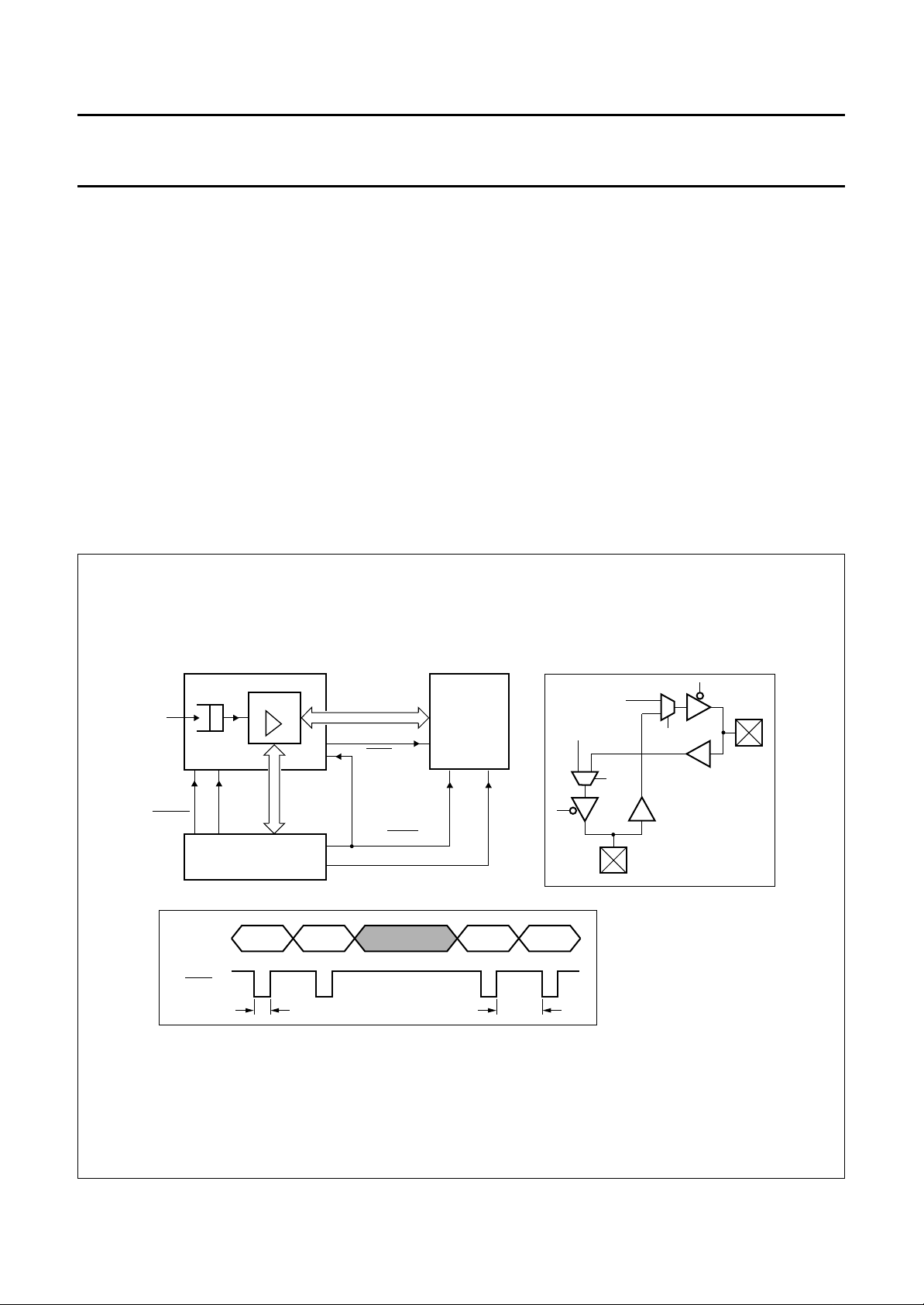
7.8 Interfacing to SAA2500 and third party audio decoders
The audio interface performs system support for Philips
SAA2500 or third party audio decoders. The pin
assignment for the interface and a description of the
respective functions is given in Table 6. Audio PES or
elementary stream data are filtered by the audio data filter
and passed to a 6 kByte FIFO buffer in which they are
stored at the byte clock frequency (9 MHz). Audio
elementary stream data is read from the FIFO at the
AUDATCLK frequency. The frequency of this clock is
adapted to the audio bit rate index (32 to 448 kbit/s), which
is derived from audio frame header information. However,
to compensate for decoder delays, the output process is
conditioned to synchronize to presentation time stamps
(PTS).
The AUDECLK output is derived from the 27 MHz
demultiplexer chip clock through division by a real
number M, which is generated by programming I0 and I1
(words: ‘audio_incr0’, ‘audio_incr1’, addresses 0x060B
and 0x060C, see Table 13). The AUDECLK can be used
as an audio decoder chip clock and is generated by the
circuitry illustrated in Fig.14. The decoder clock is
generated with a maximum edge jitter of 37/2 = 18.5 ns.
Therefore, if this clock is used for audio digital-to-analog
conversion, for high quality audio it may have to be
dejittered using an external PLL or an LC filter.
Since most audio decoders accept only elementary audio
data, the demultiplexer takes care of the following basic
tasks in the audio path:
• Parsing of audio transport packets with the proper PID
• Suppression of transport packet header data
• Detection of PES packet boundaries to find PES packet
length and PTS time stamps
• Suppression of PES headers and stuffing bytes (bit
‘audio_pes’, address 0x060A, see Table 13), optional
• Detection of audio frame boundaries to find audio frame
length and audio bit rate, optional
• Delay compensation and expansion of audio data to the
correct time and bit rate (bit ‘uc_sw_sync’, address
0x060A, see Table 13), optional.
A block diagram of the audio interface circuitry is illustrated
in Fig.15.
One basic function of the audio data filter is to optionally
determine the audio frame length and find the frame
boundaries. The audio frame length depends on the basic
audio sampling frequency, the coded bit rate, the MPEG
layer used and in case of 44.1 kHz sampling frequency,
the padding bit. The frame length ranges between
32 and 1728 bytes. All frame length related data are
coded in the audio frame header directly after the sync
word. Since the 12-bit sync word is not unique and could
be emulated in the audio stream, a recursive detection
algorithm consisting of the following steps is implemented:
1. Detect first occurrence of sync word
2. Evaluate header and determine frame length
3. If frame length is non valid go to step 1
4. Check whether a sync word exists at frame length
distance in the stream
5. If no valid sync word is detected at this position go to
step 1
6. If sync word is valid go to step 2.
All relevant header parameters are stored in dedicated
registers. Their value is used for internal control but can
also be accessed by the external microcontroller (words:
‘audio_frame_length’, ‘audio_frame_info’, addresses
0x0611 and 0x0612, see Table 13).
The delay of the audio data from input to output of the
FIFO is basically determined by PTS time stamps. In order
to avoid difficult PTS management these time stamps are
stored in the FIFO between consecutive audio frames
(see Fig.15). If a PTS exists for one specific audio frame
the 23 least significant bits of the 33-bit time stamp are
stored together with a PTS_valid flag in three byte
positions preceding the associated audio frame. If no PTS
is available, three bytes are also inserted preceding the
audio frame, but in this case the PTS_valid flag indicates
that the remaining 23 bits may not be interpreted as a valid
PTS (see Fig.15).
The input process to the audio FIFO operates in stand
alone, but can be restarted by the microcontroller
(bit ‘µc_frc_restart’, address 0x060A, see Table 13).
During restart, the write address counter is reset to 0 and
kept at this position until the first audio frame with a valid
PTS is available from the stream. The storage of PTS plus
elementary audio data is then started. The storage
process continues as long as the detected audio frame
length remains the same. If a change in frame length
occurs, or if a sync word is missing, the write counter is
reset to 0 automatically and data storage is halted until a
valid audio frame with associated PTS is retrieved from the
stream. This kind of discontinuity handling is performed
unconditionally and is signalled to the external
microcontroller (interrupt: ‘irpt_audio_restart’, address
0x0000, see Table 13).
1997 Jan 21 25

Philips Semiconductors Preliminary specification
MPEG-2 systems demultiplexer SAA7205H
The FIFO output process can operate in stand alone, but
it can also be controlled by the microcontroller. During
start-up the read address counter is reset to 0. After the
FIFO input process is started the first PTS is retrieved from
the first three byte positions in the FIFO. To this PTS value
a programmable offset is applied [resulting in: PTS* = PTS
- ‘audio_pts_offset’, addresses 0x060D to 0x060E (two’s
complement), see Table 13] to compensate for the delay
of the audio decoder. The FIFO output process is
subsequently put on hold as long as the System Time
Clock (STC) counter has not reached the value of PTS*.
When the STC counter exceeds the PTS* position the
output process is started and audio data is retrieved from
the FIFO at a speed indicated by the bit rate parameter in
the frame header (32 to 448 kbit/s).Only valid audio data is
passed to the output. Each time a valid PTS occurs at the
FIFO output the difference between PTS* and STC is
calculated and stored, to enable reading by the
microcontroller (words: ‘audio_stc_min_epts’, addresses
0x060F to 0x0611, see Table 13). Two modes of
operation can be selected by the microcontroller (bit
‘µc_free_run’, address 0x060A, see Table 13):
• PTS controlled: (‘µc_free_run’ = 0) the output process is
put on hold if PTS* is greater than the STC counter
position. Otherwise the output process continues at the
given bit-rate. In this mode, the output process could be
halted for every valid PTS which is being output by the
FIFO.
• Free running: (uc_free_run = 1) the output process is
synchronized once during start-up only and continues at
the derived bit rate without resynchronizing to new PTS
time stamps. The difference between PTS* and the STC
value is sampled and stored at the moment a PTS is
taken from the FIFO (words: ‘audio_stc_min_epts’,
addresses 0x060F to 0x0611, see Table 13). This event
is signalled to the microcontroller (interrupt:
‘irpt_audio_diff’, address 0x0000, see Table 13).
A decision for a restart (bit ‘µc_frc_restart’, address
0x060A, see Table 13) can consequently be taken in
software, whenever the difference ‘audio_stc_min_epts’
exceeds a certain audible threshold (20 ms for
instance).
After the input process is started a continuous check is
performed on the distance between the FIFO read and
write counters. If one pointer approaches the other one a
wrap around may take place (buffer underflow or
overflow), causing synchronization to be lost completely.
Should this occur an internal start-up (restart) is initiated
automatically and signalled to the microcontroller
(interrupt: ‘irpt_audio_restart’, address 0x0000,
see Table 13).
If a third party audio decoder is capable of adjusting the
output delay by itself, the demultiplexer audio output
process does not have to be PTS controlled. In this case
the functionality of the demultiplexer audio interface can
optionally be reduced to (bit ‘µc_sw_sync’ = 1, address
0x060A, see Table 13):
• Parsing of audio transport packets with the proper PID
• Suppression of transport packet header data
• Detection of PES packet borders to find PES packet
length and PTS time stamps
• Suppression of PES headers and stuffing bytes (bit
‘audio_pes’, address 0x060A, see Table 13), optional
• Time expansion of the audio transport packet payload.
In this so called software sync mode (‘µc_sw_sync’ = 1)
the FIFO input runs freely. Either entire PES packets (bit
‘audio_pes’ = 1, address 0x060A, see Table 13), or the
payload of selected PES packets is stored in the FIFO at
subsequent addresses starting from 0 at start-up.
PTS information is stored in the FIFO but is also available
in registers to make it accessible for the microcontroller
(words: ‘audio_pts’, addresses 0x0601 to 0x0602,
see Table 13).
In the software sync mode, the FIFO output process is
controlled by the microcontroller. The read address
counter is reset to 0 during start-up and stays at this
position until the write address exceeds the read address.
This is the case immediately after the input process starts.
The output process subsequently starts reading data at a
fixed data rate of 9 Mbit/s (AUDATCLK = 9 MHz, 67% duty
cycle (see Table 6 and Fig.10). The output process
continues outputting data as long as the read address
does not exceed the write address. If the read address
equals the write address the output stops (AUDATV is set
to logic 0) until new data is received at the input and the
write address counter increments again. Consequently, if
audio transport packets are equally distributed along the
transport stream, the FIFO remains almost empty.
The FIFO cannot overflow if the output rate equals at least
the average input rate. Given a capacity of 6 kByte for the
FIFO this means that at least 30 audio transport packets
can be stored before an overflow occurs.
Audio data can be downloaded by the microcontroller to
enable generation of ‘beeps’. For this purpose, the
demultiplexer has to be set to download mode (bit
‘µc_downl’ = 1, address 0x060A, see Table 13).
1997 Jan 21 26
 Loading...