

Philips SAA7201H-B-C2, SAA7201H-C1, SAA7201H-C1-S1, SAA7201H-C2, SAA7201H-C2-R1 Datasheet
...
DATA SH EET
Objective specification
File under Integrated Circuits, IC02
1997 Jan 29
INTEGRATED CIRCUITS
SAA7201
Integrated MPEG2 AVG decoder

1997 Jan 29 2
Philips Semiconductors Objective specification
Integrated MPEG2 AVG decoder SAA7201
FEATURES
General
• Uses single external Synchronous DRAM (SDRAM)
organized as 1M × 16 interfacing at 81 MHz; compatible
with the SDRAM ‘lite’ or ‘PC’
• Fast external CPU interface; 16-bit data + 8-bit address
• Dedicated input for audio and video data in PES or ES
format; data input rate: ≤9 Mbytes/s in byte mode;
≤20 Mbit/s in bit serial mode; audio and/or video data
can also serve as input via CPU interface
• Single 27 MHz external clock for time base reference
and internal processing; all required decoding and
presentation clocks are generated internally
• Internal system time base at 90 kHz can be
synchronized via CPU port
• Flexible memory allocation under control of the external
CPU enables optimized partitioning of memory for
different tasks
• Boundary scan (JTAG) plus external SDRAM self test
implemented
• Supply voltage 3.3 V
• Package 160 QFP.
CPU relation
• 16-bit data, 8-bit address, or 16-bit multiplexed bus;
Motorola and Intel mode supported
• Support for fast DMA transfer to either internal registers
or external SDRAM
• Maximum sustained rate to the external SDRAM is
9 Mbytes/s.
MPEG2 system
• Parsing of MPEG2 PES and MPEG1 packet streams
• Double System Time Clock (STC) counters for
discontinuity handling
• Time stamps or CPU controlled audio/video
synchronization
• Support for seamless time base change (edition)
• Processing of errors flagged by channel decoding or
demux section
• Support for retrieval of PES header and PES private
data.
MPEG2 audio
• Decoding of 2 channel, layer I and II MPEG audio;
support for mono, stereo, intensity stereo and dual
channel mode
• Constant and variable bit rates up to 448 kbit/s
• Audio sampling frequencies: 48, 44.1, 32, 24, 22.05 and
16 kHz
• CRC error detection
• Selectable output channel in dual channel mode
• Independent volume control for both channels and
programmable inter-channel crosstalk control through a
baseband audio processing unit
• Storage ancillary data up to 54 bytes
• Dynamic range control at output
• Muting possibility via external controller; automatic
muting in case of errors
• Generation of ‘beeps’ with programmable tone height,
duration and amplitude
• Serial two channel digital audio output with 16, 18, 20 or
22 bits per sample, compatible with either I2S or
Japanese formats
• Serial SPDIF audio output
• Clock output 256 or 384 × fs for external D/A converter
• Audio input buffer in external SDRAM with
programmable size (default is 64 kbit)
• Programmable processing delay compensation
• Software controlled stop, pause, restricted skip, and
restart functions.
MPEG2 video
• Decoding of MPEG2 video up to main level, main profile
• Nominal video input buffer size equals 2.6 Mbit for Video
Main Profile and Main Level (MP@ML)
• Output picture format: CCIR-601 4 : 2 : 2 interlaced
pictures; picture format 720 × 576 at 50 Hz or 720 × 480
at 60 Hz
• 3 : 2 pull-down supported with 24 and 30 Hz sequences
• Support of constant and variable bit rates up to 15 Mbit/s
• Output interface at 8-bit wide, 27 MHz UYVY
multiplexed bus
• Horizontal and vertical pan and scan allows the
extraction of a window from the coded picture

1997 Jan 29 3
Philips Semiconductors Objective specification
Integrated MPEG2 AVG decoder SAA7201
• Flexible horizontal continuous scaling from 0.5 up to 4
allows easy aspect ratio conversion including support
for 2.21 : 1 aspect ratio movies
• Vertical scaling with fixed factors 0.5, 1 or 2 to support
picture scaling and up-sampling
• Scaling of incoming pictures to 25% of their original size
with anti-aliasing filtering to free screen space for
graphics applications like electronic program guides
• Non-full screen MPEG pictures will be displayed in a box
of which position and background colour are adjustable
by the external CPU
• Video output may be slaved to internally (master)
generated or externally (slave) supplied HV
synchronization signals; the position of active video is
programmable; MPEG timebase changes do not
affected the display phase
• Video output direct connectable to SAA718X encoder
family
• Various trick modes under control of external CPU:
– Freeze I or P pictures; restart on I picture
– Freeze on B pictures; restart at any moment
– Scanning and decoding of I or I and P pictures
– Single step mode
– Repeat/Skip field for time base correction.
Graphics
• Graphics is region based and presented in boxes
independent of video format
• Screen arrangement of boxes is determined by display
list mechanism which allows for multiple boxes,
background loading, fast switching, scrolling and fading
of regions
• Support of 2, 4, 8 bits/pixel bit-maps in fixed bit-maps or
coded in accordance to the DVB variable/run length
standard for region bases graphics
• Optimized memory control in MPEG video decoding
allows for storage of graphical bit-maps up to 1.2 Mbit in
50 Hz and 2.0 Mbit in 60 Hz systems
• VL/RL encoding enables full screen graphics at
8 bit/pixel in 50 Hz
• Fast CPU access enables full bit-map updates within a
display field period
• Display colours are obtained via colour look-up tables;
CLUT output is YUVT at 8-bit for each signal component
thus enabling 16M different colours and 6-bit for T
(transparency) which gives 64 mixing levels with video
• Bit-map table mechanism to specify a sub-set of entries
if the CLUT is larger than required by the coded bit
pattern; supported bit-map tables are 16 to 256,
4 to 256 and 4 to 16
• Graphics boxes may not overlap vertically; if 256 entry
CLUT has to be down loaded, a vertical separation of
1 field line is mandatory
• Internal support for fast block moves in the external
SDRAM during MPEG decoding
• Graphics mechanism can be used for signal generation
in the vertical blanking interval; useful for teletext, wide
screen signalling, closed caption etc.
• Support for a single down-loadable cursor of 1 kpixel
with programmable shape; supported shapes are
8 × 128, 16 × 64, 32 × 32, 64 × 16 and 128 × 8
• Cursor colours are determined via a 4-entry CLUT with
YUVT at 6, 4, 4 respectively 2 bits; mixing of cursor with
video + graphics in 4 levels
• Cursor can be moved freely across the screen without
overlapping restrictions.
1997 Jan 29 4
Philips Semiconductors Objective specification
Integrated MPEG2 AVG decoder SAA7201
GENERAL DESCRIPTION
The SAA7201 is an MPEG2 decoder which combines
audio decoding and video decoding. Additionally to these
basic MPEG functions it also provides means for
enhanced graphics and/or on-screen display.
Due to an optimized architecture for audio and video
decoding, maximum capacity in the external memory and
processing power from the external CPU is available for
the support for graphics.
QUICK REFERENCE DATA
ORDERING INFORMATION
SYMBOL PARAMETER MIN. TYP. MAX. UNIT
V
DD
functional supply voltage 3.0 3.3 3.6 V
V
CC
pad supply voltage 3.0 3.3 3.6 V
I
DD(tot)
total supply current at VDD= 3.3 V − tbf − mA
f
CLK
clock frequency − 27.0 − MHz
∆f
CLK
frequency deviation −30 × 10−6− +30 × 10
−6
TYPE
NUMBER
PACKAGE
NAME DESCRIPTION VERSION
SAA7201H QFP160 plastic quad flat package; 160 leads (lead length 1.95 mm);
body 28 × 28 × 3.4 mm; high stand-off height
SOT322-4
1997 Jan 29 5
Philips Semiconductors Objective specification
Integrated MPEG2 AVG decoder SAA7201
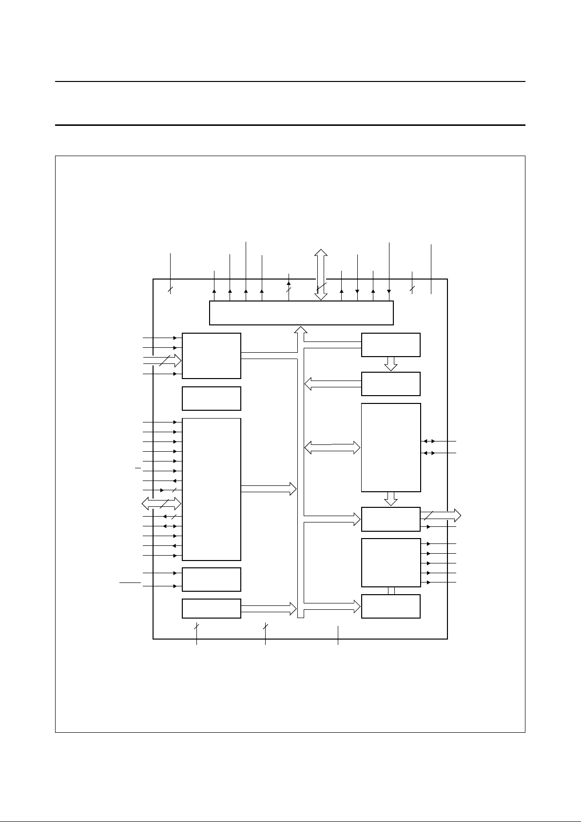
BLOCK DIAGRAM
Fig.1 Block diagram.
handbook, full pagewidth
AUDIO/VIDEO
INTERFACE
HOST
INTERFACE
SYSTEM TIME
BASE UNIT
VIDEO INPUT
BUFFER & SYNC
MEMORY
INTERFACE
VIDEO
DECODER
GRAPHICS
UNIT
AUDIO INPUT
BUFFER & SYNC
CLOCK
GENERATION
JTAG
MGD322
159
A_STROBE
77 75 74 78 84 83 81 80
SDRAM_RAS
V
DDCO1
to
V
DDCO4
SDRAM_WE
CP81M READ
O
READ
I
SDRAM_ADDR
(11 to 0)
SDRAM_DATA
(15 to 0)
SDRAM_CAS SDRAM_UDQ CP81MEXT
CPU_TYPE
DMA_REQ
DMA_ACK
DMA_RDY
DMA_DONE
V_STROBE
ERROR
MUX
HS
VS
106
107
CS
DS
AS
R/W
DTACK
ADDRESS(8 to 1)
DATA(15 to 0)
IRQ(3 to 0)
AV_DATA(0 to 7)
2
1
8
CLK
124
RESET
138
9
10
4
4
3
6
5
DISPLAY
UNIT
SD
SCLK
WS
SPDIF
143
142
145
146
AUDIO
DECODER
GRPH
YUV(7 to 0)
119
FSCLK
139
11
12
8
148
147
8
16
8
16
12
4
SAA7201
V
SSCO1
to V
SSCO4
4
V
SS1
to V
SS16
16
V
SSA
122
V
DD1
to
V
DD16
16
V
DDA
121

1997 Jan 29 6
Philips Semiconductors Objective specification
Integrated MPEG2 AVG decoder SAA7201
PINNING
SYMBOL PIN DESCRIPTION V I/O
MUX 1 multiplexed/non-multiplexed (active LOW) bus input 5.0 I
CPU_TYPE 2 Intel/Motorola (active LOW) selection input 5.0 I
DMA_ACK 3 DMA acknowledge input 3.3 I
DMA_REQ 4 DMA request input and output 3.3 I/O
DMA_DONE 5 DMA end input 3.3 I
DMA_RDY 6 DMA ready output 3.3 O/Z
V
SS1
7 ground for pad ring 3.3 −
CS 8 chip select input 5.0 I
DS 9 data strobe input 5.0 I
AS 10 address strobe input 5.0 I
R/W 11 read/write (active LOW) input 5.0 I
DTACK 12 data acknowledge output 5.0 O/Z
V
DD1
13 supply for pad ring 3.3 −
IRQ0 14 individually maskable interrupts 3.3 O/Z
IRQ1 15 individually maskable interrupts 3.3 O/Z
IRQ2 16 individually maskable interrupts 3.3 O/Z
IRQ3 17 individually maskable interrupts 3.3 O/Z
V
SS2
18 ground for pad ring − −
V
SSCO1
19 ground for core logic − −
V
DDCO1
20 supply for core logic 3.3 −
DATA0 21 CPU data interface 5.0 I/O
DATA1 22 CPU data interface 5.0 I/O
DATA2 23 CPU data interface 5.0 I/O
DATA3 24 CPU data interface 5.0 I/O
V
DD2
25 supply for pad ring 3.3 −
DATA4 26 CPU data interface 5.0 I/O
DATA5 27 CPU data interface 5.0 I/O
DATA6 28 CPU data interface 5.0 I/O
DATA7 29 CPU data interface 5.0 I/O
V
SS3
30 ground for pad ring − −
DATA8 31 CPU data interface 5.0 I/O
DATA9 32 CPU data interface 5.0 I/O
DATA10 33 CPU data interface 5.0 I/O
DATA11 34 CPU data interface 5.0 I/O
V
DD3
35 supply for pad ring − −
DATA12 36 CPU data interface 5.0 I/O
DATA13 37 CPU data interface 5.0 I/O
DATA14 38 CPU data interface 5.0 I/O
DATA15 39 CPU data interface 5.0 I/O
V
SS4
40 ground for pad ring − −

1997 Jan 29 7
Philips Semiconductors Objective specification
Integrated MPEG2 AVG decoder SAA7201
ADDRESS1 41 CPU address interface 5.0 I
ADDRESS2 42 CPU address interface 5.0 I
ADDRESS3 43 CPU address interface 5.0 I
ADDRESS4 44 CPU address interface 5.0 I
V
DD4
45 supply for pad ring 3.3 −
ADDRESS5 46 CPU address interface 5.0 I
ADDRESS6 47 CPU address interface 5.0 I
ADDRESS7 48 CPU address interface 5.0 I
ADDRESS8 49 CPU address interface 5.0 I
V
SS5
50 ground for pad ring − −
V
SSCO2
51 ground for core logic − −
V
DDCO2
52 supply for core logic 3.3 −
SDRAM_DATA0 53 memory data interface 3.3 I/O
SDRAM_DATA15 54 memory data interface 3.3 I/O
SDRAM_DATA1 55 memory data interface 3.3 I/O
V
DD5
56 supply for pad ring 3.3 −
SDRAM_DATA14 57 memory data interface 3.3 I/O
SDRAM_DATA2 58 memory data interface 3.3 I/O
SDRAM_DATA13 59 memory data interface 3.3 I/O
V
SS6
60 ground for pad ring − −
SDRAM_DATA3 61 memory data interface 3.3 I/O
SDRAM_DATA12 62 memory data interface 3.3 I/O
SDRAM_DATA4 63 memory data interface 3.3 I/O
V
DD6
64 supply for pad ring 3.3 −
SDRAM_DATA11 65 memory data interface 3.3 I/O
SDRAM_DATA5 66 memory data interface 3.3 I/O
SDRAM_DATA10 67 memory data interface 3.3 I/O
V
SS7
68 ground for pad ring − −
SDRAM_DATA6 69 memory data interface 3.3 I/O
SDRAM_DATA9 70 memory data interface 3.3 I/O
SDRAM_DATA7 71 memory data interface 3.3 I/O
V
DD7
72 supply for pad ring 3.3 −
SDRAM_DATA8 73 memory data interface 3.3 I/O
SDRAM_WE 74 SDRAM write enable output 3.3 O
SDRAM_CAS 75 SDRAM column address strobe output 3.3 O
V
SS8
76 ground for pad ring − −
SDRAM_RAS 77 SDRAM row address strobe output 3.3 O
SDRAM_UDQ 78 SDRAM write mask output 3.3 O
V
DD8
79 supply for pad ring 3.3 −
READ
I
80 read command input 3.3 I
SYMBOL PIN DESCRIPTION V I/O

1997 Jan 29 8
Philips Semiconductors Objective specification
Integrated MPEG2 AVG decoder SAA7201
READ
O
81 read command output 3.3 O
V
SS9
82 ground for pad ring − −
CP81MEXT 83 81 MHz clock return path input 3.3 I
CP81M 84 81 MHz memory clock output 3.3 O
V
DD9
85 supply for pad ring 3.3 −
SDRAM_ADDR8 86 memory address 3.3 O
SDRAM_ADDR9 87 memory address 3.3 O
SDRAM_ADDR11 88 memory address 3.3 O
V
SS10
89 ground for pad ring − −
SDRAM_ADDR7 90 memory address 3.3 O
SDRAM_ADDR10 91 memory address 3.3 O
SDRAM_ADDR6 92 memory address 3.3 O
V
DD10
93 supply for pad ring 3.3 −
SDRAM_ADDR0 94 memory address 3.3 O
SDRAM_ADDR5 95 memory address 3.3 O
SDRAM_ADDR1 96 memory address 3.3 O
V
SS11
97 ground for pad ring − −
SDRAM_ADDR4 98 memory address 3.3 O
SDRAM_ADDR2 99 memory address 3.3 O
SDRAM_ADDR3 100 memory address 3.3 O
V
SSCO3
101 ground for core logic − −
V
DDCO3
102 supply for core logic 3.3 −
V
DD11
103 supply for pad ring 3.3 −
TEST8 104 IC test interface 3.3 I/O
TEST7 105 IC test interface 3.3 I/O
HS 106 horizontal synchronization input and output 3.3 I/O
VS 107 vertical synchronization input and output 3.3 I/O
V
SS12
108 ground for pad ring − −
YUV0 109 YUV video output at 27 MHz 3.3 O/Z
YUV1 110 YUV video output at 27 MHz 3.3 O/Z
YUV2 111 YUV video output at 27 MHz 3.3 O/Z
YUV3 112 YUV video output at 27 MHz 3.3 O/Z
V
DD12
113 supply for pad ring 3.3 −
YUV4 114 YUV video output at 27 MHz 3.3 O/Z
YUV5 115 YUV video output at 27 MHz 3.3 O/Z
YUV6 116 YUV video output at 27 MHz 3.3 O/Z
YUV7 117 YUV video output at 27 MHz 3.3 O/Z
TEST6 118 IC test interface 3.3 I/O
GRPH 119 indicator for graphics information output 3.3 O
TEST5 120 IC test interface 3.3 I/O
SYMBOL PIN DESCRIPTION V I/O

1997 Jan 29 9
Philips Semiconductors Objective specification
Integrated MPEG2 AVG decoder SAA7201
V
DDA
121 supply for analogue blocks 3.3 −
V
SSA
122 ground for analogue blocks − −
V
SS13
123 ground for pad ring − −
CLK 124 27 MHz clock input 3.3 I
V
SS14
125 ground for pad ring − −
TCLK 126 boundary scan test clock input 3.3 I
TRST 127 boundary scan test reset input 3.3 I
TMS 128 boundary scan test mode select input 3.3 I
TD
O
129 boundary scan test data output 3.3 O
TD
I
130 boundary scan test data input 3.3 I
V
DD13
131 supply for pad ring 3.3 −
TEST4 132 IC test interface 3.3 I/O
TEST3 133 IC test interface 3.3 I/O
TEST2 134 IC test interface 3.3 I/O
TEST1 135 IC test interface 3.3 I/O
TEST0 136 IC test interface 3.3 I/O
V
DD14
137 supply for pad ring 3.3 −
RESET 138 hard reset input (active LOW) 3.3 I
FSCLK 139 256 or 384 fs (audio sampling) output 3.3 O/Z
V
DDCO4
140 supply for core logic 3.3 −
V
SSCO4
141 ground for core logic − −
SCLK 142 serial audio clock output 3.3 O/Z
SD 143 serial audio data output 3.3 O/Z
V
SS15
144 ground for pad ring − −
WS 145 word select output 3.3 O/Z
SPDIF 146 digital audio output 3.3 O/Z
ERROR 147 flag for bitstream error input 5.0 I
V_STROBE 148 video strobe input 5.0 I
V
DD15
149 supply for pad ring 3.3 −
AV_DATA0 150 MPEG input port for PES data 5.0 I
AV_DATA1 151 MPEG input port for PES data 5.0 I
AV_DATA2 152 MPEG input port for PES data 5.0 I
AV_DATA3 153 MPEG input port for PES data 5.0 I
V
SS16
154 ground for pad ring − −
AV_DATA4 155 MPEG input port for PES data 5.0 I
AV_DATA5 156 MPEG input port for PES data 5.0 I
AV_DATA6 157 MPEG input port for PES data 5.0 I
AV_DATA7 158 MPEG input port for PES data 5.0 I
A_STROBE 159 audio strobe input 5.0 I
V
DD16
160 supply for pad ring 3.3 −
SYMBOL PIN DESCRIPTION V I/O

1997 Jan 29 10
Philips Semiconductors Objective specification
Integrated MPEG2 AVG decoder SAA7201
Fig.2 Pin configuration.
handbook, full pagewidth
MGD321
SAA7201
1
2
3
4
5
6
7
8
9
10
11
12
13
14
15
16
17
18
19
20
21
22
23
24
25
26
27
28
29
30
31
32
33
34
35
36
37
38
39
40
MUX
CPU_TYPE
DMA_ACK
DMA_REQ
DMA_DONE
DMA_RDY
V
SS1
CS
DS
AS
R/W
DTACK
V
DD1
IRQ0
IRQ1
IRQ2
IRQ3
V
SS2
V
SSCO1
V
DDCO1
DATA0
DATA1
DATA2
DATA3
V
DD2
DATA4
DATA5
DATA6
DATA7
V
SS3
DATA8
DATA9
DATA10
DATA11
V
DD3
DATA12
DATA13
DATA14
DATA15
V
SS4
120
119
118
117
116
115
114
113
112
111
110
109
108
107
106
105
104
103
102
101
100
99
98
97
96
95
94
93
92
91
90
89
88
87
86
85
84
83
82
81
160
159
158
157
156
155
154
153
152
151
150
149
148
147
146
145
144
143
142
141
140
139
138
137
136
135
134
133
132
131
130
129
128
127
126
125
124
123
122
121
414243444546474849505152535455565758596061626364656667686970717273747576777879
80
TEST5
GRPH
TEST6
YUV7
YUV6
YUV5
YUV4
V
DD12
YUV3
YUV2
YUV1
YUV0
V
SS12
VS
HS
TEST7
TEST8
V
DD11
V
DDCO3
V
SSCO3
SDRAM_ADDR3
SDRAM_ADDR2
SDRAM_ADDR4
V
SS11
SDRAM_ADDR1
SDRAM_ADDR5
SDRAM_ADDR0
V
DD10
SDRAM_ADDR6
SDRAM_ADDR10
SDRAM_ADDR7
V
SS10
SDRAM_ADDR11
SDRAM_ADDR9
SDRAM_ADDR8
V
DD9
CP81M
CP81MEXT
V
SS9
READ
O
V
DD16
A_STROBE
AV_DATA7
AV_DATA6
AV_DATA5
AV_DATA4
V
SS16
AV_DATA3
AV_DATA2
AV_DATA1
AV_DATA0
V
DD15
V_STROBE
ERROR
SPDIFWSV
SS15
SD
SCLK
V
SSCO4VDDCO4
FSCLK
RESET
V
DD14
TEST0
TEST1
TEST2
TEST3
TEST4
V
DD13
TDITDOTMS
TRST
TCLK
V
SS14
CLK
V
SS13VSSAVDDA
ADDRESS1
ADDRESS2
ADDRESS3
ADDRESS4
V
DD4
ADDRESS5
ADDRESS6
ADDRESS7
ADDRESS8
V
SS5
V
SSCO2
V
DDCO2
SDRAM_DATA0
SDRAM_DATA15
SDRAM_DATA1
V
DD5
SDRAM_DATA14
SDRAM_DATA2
SDRAM_DATA13
V
SS6
SDRAM_DATA3
SDRAM_DATA12
SDRAM_DATA4
V
DD6
SDRAM_DATA11
SDRAM_DATA5
SDRAM_DATA10
V
SS7
SDRAM_DATA6
SDRAM_DATA9
SDRAM_DATA7
V
DD7
SDRAM_DATA8
SDRAM_WE
SDRAM_CAS
V
SS8
SDRAM_RAS
SDRAM_UDQ
V
DD8
READ
I
1997 Jan 29 11
Philips Semiconductors Objective specification
Integrated MPEG2 AVG decoder SAA7201
FUNCTIONAL DESCRIPTION
General
The SAA7201 is an MPEG2 decoder which combines
audio decoding, video decoding and enhanced region
based graphics. The decoder operates with a single
16 Mbit external synchronous dynamic random access
memory (SDRAM) and runs from a single external 27 MHz
clock. Due to the optimized memory control for MPEG2
decoding, more than 1 Mbit is available for graphics in
50 Hz systems.
MPEG2 data can be accepted up to 9 Mbytes/s through a
dedicated byte wide interface. The data on this interface
can be either in PES (Packetized Elementary Stream),
MPEG1 packet or ES (Elementary Stream) format as
described in Chapter “References”. Two additional strobe
signals distinguish between audio and video data.
The internal video decoder is capable of decoding all
MPEG compliant streams up to main level main profile as
specified in Chapter “References”. The audio decoder
implements 2 channel audio decoding according to the
standards in Chapter “References”.
All real time audio/video decoding and synchronization
tasks are performed autonomously, so the external
microcontroller only needs to perform high-level tasks like
initialization, status monitoring and trick mode control.
The main support task of the external microcontroller
concerns the control of the graphical unit. This unit should
be supplied with bit-maps, determining the contents of the
graphical regions and by a simple set of instructions
determining the appearance of the graphical data on the
screen. Most graphical information should be stored in the
external memory which implies multiple data transfers
between CPU and the external memory. By performing
these data transfers on a direct memory access (DMA)
basis, full bit-maps can be transferred within one video
frame period.
The video output, containing a mix of MPEG video and
graphical data, is at a YUV multiplexed format which can
be directly connected to an external composite video
encoder. The audio output, containing a mix of MPEG
audio and programmable ‘beeps’, is in a serial, I2S or
Japanese format which can be directly supplied to most
commercially available up-sampling audio DA converters.
A functional block diagram of the decoder is given in Fig.1.
Its application environment is depicted in Fig.24. In the
following sections, a brief description of the individual
internal blocks of the MPEG2 decoder will be given.
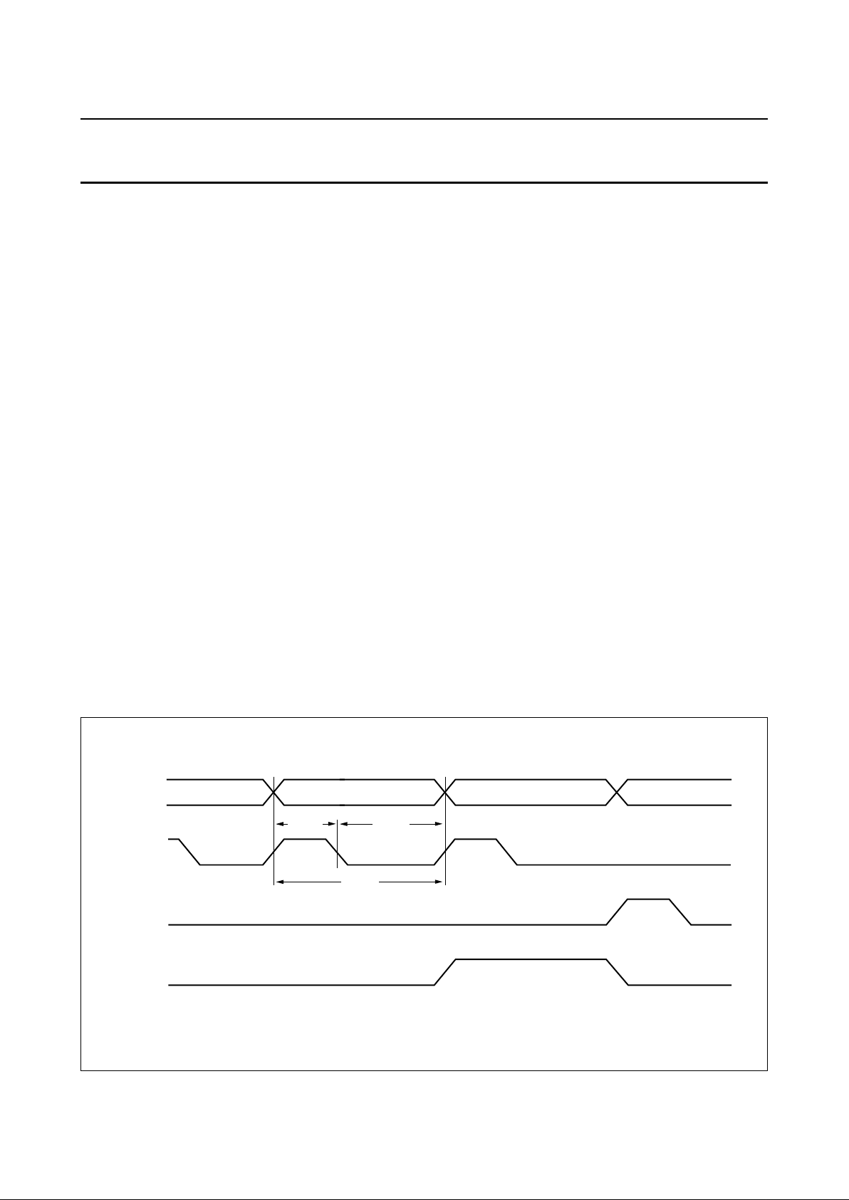
Audio/video interface
In a basic set-top box application the SAA7201 receives
audio and video PES data in a byte wide format at rates up
to 9 Mbytes/s. A timing diagram is shown in Fig.3. Next to
the 8-bit wide data bus an audio and video strobe is
expected at the input. Erroneous data may be flagged via
the error indicator.
handbook, full pagewidth
V_STROBE
A_STROBE
ERROR
AV_DATA
(0 to 7)
≥25 ns ≥25 ns
≥111 ns
video byte (n) video byte (n + 1) audio byte (m)
MGD323
Fig.3 Timing diagram of parallel input mode.
 Loading...