

Philips saa7196 DATASHEETS
INTEGRATED CIRCUITS
DATA SH EET
SAA7196
Digital video decoder, Scaler and
Clock generator circuit (DESCPro)
Product specification
File under Integrated Circuits, IC22
1996 Nov 04

Philips Semiconductors Product specification
Digital video decoder, Scaler and Clock
generator circuit (DESCPro)
CONTENTS
1 FEATURES
2 GENERAL DESCRIPTION
3 QUICK REFERENCE DATA
4 ORDERING INFORMATION
5 BLOCK DIAGRAM
6 PINNING
7 FUNCTIONAL DESCRIPTION
7.1 Decoder part
7.1.1 Chrominance processor
7.1.2 Luminance processor
7.1.3 Synchronization
7.2 Expansion port (see Fig.2)
7.3 Monitor controls BCS (see Fig.2)
7.3.1 Brightness and contrast controls; see
Tables 1 and 2
7.3.2 Saturation control; see Table 3
7.3.3 RTCO output pin 44 (see Fig.11)
7.3.4 RTS1 and RTS0 outputs (pins 34 and 35)
7.4 Scaler part
7.4.1 Decimation filters
7.4.2 Vertical processing (VPU_Y)
7.4.3 RGB matrix
7.4.3.1 Anti-gamma ROM tables
7.4.4 Chrominance signal keyer
7.4.5 Scale control and vertical regions
7.4.5.1 Vertical bypass region
7.4.5.2 Vertical scaling region
7.4.5.3 Vertical regions (see Fig.12)
7.4.6 Output data representation and levels
7.4.7 Output FIFO register and VRAM port
7.4.8 VRAM port transfer procedures
7.4.9 Data burst transfer mode
7.4.10 Transparent data transfer mode
7.4.10.1 Interlaced processing
(OF bits, subaddress 20)
7.4.10.2 INCADR timing
7.4.10.3 Monochrome format (see Table 10)
7.4.10.4 VRAM port specifications
7.4.11 Field processing
7.4.12 Operation cycle
7.5 Power-on reset
8 PROGRAMMING MODEL
8.1 I2C-bus format
8.2 I2C-bus status information
8.3 Decoder part
8.4 Scaler part
SAA7196
9 LIMITING VALUES
10 CHARACTERISTICS
11 PROCESSING DELAYS
12 APPLICATION INFORMATION
12.1 Programming example
13 PACKAGE OUTLINE
14 SOLDERING
14.1 Introduction
14.2 Reflow soldering
14.3 Wave soldering
14.4 Repairing soldered joints
15 DEFINITIONS
16 LIFE SUPPORT APPLICATIONS
17 PURCHASE OF PHILIPS I2C COMPONENTS
1996 Nov 04 2

Philips Semiconductors Product specification
Digital video decoder, Scaler and Clock
generator circuit (DESCPro)
1 FEATURES
• Digital 8-bit luminance input [video (Y) or CVBS]
• Digital 8-bit chrominance input [CVBS or C from CVBS,
Y/C, S-Video (S-VHS or Hi8)]
• Luminance and chrominance signal processing for main
standards PAL, NTSC and SECAM
• Horizontal and vertical sync detection for all standards
• User programmable luminance peaking for aperture
correction
• Compatible with memory-based features (line-locked
clock, square pixel)
• Cross colour reduction by chrominance comb-filtering
for NTSC or special cross-colour cancellation for
SECAM
• UV signal delay lines for PAL to correct chrominance
phase errors
• Square-pixel format with 768/640 active samples per
line
• The bidirectional expansion port (YUV-bus) supports
data rates of 780 × f
SECAM) in 4 :2:2 format
• Brightness, contrast, hue and saturation controls for
scaled outputs
• Down-scaling of video windows with 1023 active
samples per line and 1023 active lines per frame to
randomly sized windows
• 2D data processing for improved signal quality of scaled
luminance data, especially for compression applications
• Chroma key (α-generation)
• YUV to RGB conversation including anti-gamma
ROM tables for RGB
• 16-word output FIFO (32-bit words)
• Output configurable for 32-, 24- and 16-bit
video data bus
• Scaled 16-bit 4 :2:2 YUV output
• Scaled 15-bit RGB (5-5-5+α) and 24-bit (8-8-8+α)
output
• Scaled 8-bit monochrome output
• Line increment, field sequence (odd/even,
interlace/non-interlaced) and vertical reset control for
easy memory interfacing
• Output of discontinuous data bursts of scaled video data
or continuous data output with corresponding qualifier
signals
• Real-time status information
(NTSC) and 944 × fH (PAL,
H
SAA7196
2
C-bus control
• I
• Only one crystal of 26.8 MHz required
• Clock generator on chip.
2 GENERAL DESCRIPTION
The CMOS circuit SAA7196, digital video decoder, scaler
and clock generator (DESCPro), is a highly integrated
circuit for DeskTop Video applications. It combines the
functions of a digital multistandard decoder (SAA7191B),
a digital video scaler (SAA7186) and a clock generator
(SAA7197).
The decoder is based on the principle of line-locked clock
decoding. It runs at square-pixel frequencies to achieve
correct aspect ratio. Monitor controls are provided to
ensure best display.
Four data ports are supported:
• Port CVBS7 to CVBS0 of input interface; used in Y/C
mode (see Fig.1) to decode digitized luminance and
chrominance signals (digitized in two external ADCs).
In normal mode, only this input port is used and only one
ADC is necessary (see Fig.4)
• Port CHR7 to CHR0 of input interface; used in Y/C
mode (see Fig.1) to decode digitized luminance and
chrominance signals (digitized in two external ADCs)
• 32-bit VRAM output port; interface to the video memory.
It outputs the down-scaled video data; different formats
and operation modes are supported by this circuit
• 16-bit expansion port; this is a bidirectional port.
In general, it establishes the digital YUV as known from
the SAA71x1 family of digital decoders. In addition, the
expansion port is configurable to send data from the
decoder unit or to accept external data for input into the
scaler. In input mode the clock rate and/or the sync
signals may be delivered by the external data source.
Decoder and scaler units can run at different clock rates.
The decoder processing always operates with a Line
Locked Clock (LLC). This clock is derived from the CVBS
signal and is suited best for memory based video
processing; the LLC clock is always present. The scaler
clock may be driven by the LLC clock or by an external
clock depending on the configuration of the expansion
port.
1996 Nov 04 3
Philips Semiconductors Product specification
Digital video decoder, Scaler and Clock
SAA7196
generator circuit (DESCPro)
The circuit is I2C-bus controlled. The I2C-bus interface is
clocked by LLC to ensure proper control.
The I2C-bus control is identical to that of the SAA7194.
It is divided into two sections:
• Subaddress 00H to 1FH for the decoder part
(Tables 16 and 17)
• Subaddress 20H to 3FH for the scaler part
(Tables 29 and 30).
3 QUICK REFERENCE DATA
Measured over full voltage and temperature ranges.
SYMBOL PARAMETER MIN. TYP. MAX. UNIT
V
DD
I
DD(tot)
V
I
V
O
f
BCK
T
amb
supply voltage 4.5 5 5.5 V
total supply current − 180 280 mA
data input level TTL-compatible
data output level TTL-compatible
input clock frequency −−32 MHz
operating ambient temperature 0 − 70 °C
The programming of the subaddresses for the scaler part
becomes effective at the first Vertical Sync (VS) pulse after
a transmission.
4 ORDERING INFORMATION
PACKAGE
TYPE NUMBER
NAME DESCRIPTION VERSION
SAA7196H QFP120 plastic quad flat package; 120 leads (lead length 1.95 mm);
body 28 × 28 × 3.4 mm; high stand-of height
SOT349-1
1996 Nov 04 4
Philips Semiconductors Product specification
Digital video decoder, Scaler and Clock
generator circuit (DESCPro)
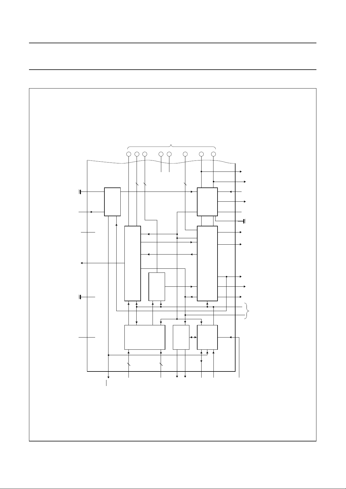
5 BLOCK DIAGRAM
B
A
C
VDDV
Y7 to Y0
8
+5 V
CTST
CGCE
15
3776, 105
HREF
UV7 to UV0
8
CGC
SAA7196
to
part
scaler
D
SS
HS, VS
2
clock A
G
CREF
H
LLC
CLOCK A
GENERATOR
F
E
MHA381
CREF
LLCXTALHCL
XT ALIRTS0RTS1LFCOHSY
1 2 40 38
+5 V
DDA
V
SSA
V
internally
connected
+5 V
44
RTCO
SSD7
to V
SSD1
16, 30, 47, 60,
V
DDD7
to V
DDD1
14, 31, 45, 61,
V
75, 104, 120
77, 91, 106
36
RES
SAA7196
DECODER PART
8
CHR7
CHROMINANCE PROCESSOR
13 to 6
to
CHR0
INPUT
INTERFACE
LUMINANCE
PROCESSOR
8
24 to 17
to
CVBS7
CVBS0
SYNC PLIN
clock
33
status
STATUS
PORT AND
32
GPSW1
REGISTER
GPSW2
SYNCHRONIZATION
C-BUS
2
I
CONTROL
3
4
SCL
SDA
26 28 34 35 29 27
25
control and
status to and
from scaler part
5
CSA
2
I
handbook, full pagewidth
Fig.1 Block diagram of decoder part (continued in Fig.2).
1996 Nov 04 5
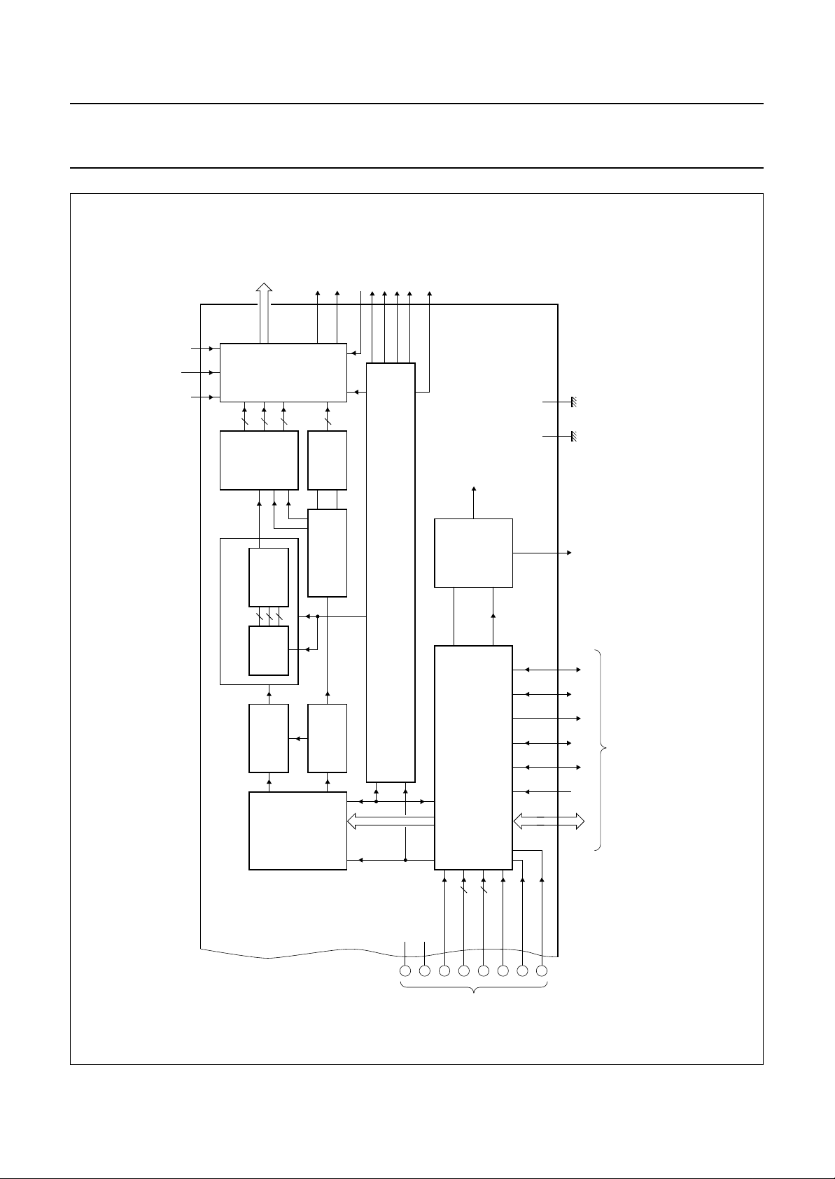
Philips Semiconductors Product specification
Digital video decoder, Scaler and Clock
generator circuit (DESCPro)
port output
RGB or YUV
VOEN
VCLK BTST
56 53 43
57 to 59
62 to 74
8
RGB
MATRIX
32-bit VRAM
VRO31 to VRO0
78 to 90
92 to 94
OUTPUT
FORMATTER
8
FOLLOWED
Y
U
BY
55
OUTPUT
8
ROMs
ANTI-GAMMA
V
U
INCADR
HFL
54
FIFO
REGISTER
15
KEYER
CHROMA
V
VMUX
SODD
SVS
SHREF
4648495051
PXQ
52
LNQ
SAA7196 SCALER PART
clock B
brightness,
to scaler and
SAA7196
MHA382
119
SP
AP
controls
contrast
saturation
VERTICAL FILTER
ARITHMETIC
LINE
(8 x 384)
MEMORY
FILTER
LUMINANCE
DECIMATION
Y
AND
CONTRAST
BRIGHTNESS
SATURATION
CHROMA
UV
CONTROLS
INTERPOLATOR
DECIMATION
(BCS)
FILTER
SCALE CONTROL
to
YUV15
VS
YUV0
HREF
VDDV
42 118
116 39117 41
95 115
YUV15 to YUV0
LLC2
CREFB
HREF HS LLCB
DIR VS
96 to 103
107 to 114
handbook, full pagewidth
expansion port
input/output
Fig.2 Block diagram of brightness, contrast, saturation controls and scaler part (continued from Fig.1).
CLOCK B
GENERATOR
LLCINB
CREFINB
BUS INTERFACE
8
8
SS
HREF
UV7 to UV0
Y7 to Y0
HS, VS
CREF
LLC
D
1996 Nov 04 6
F
B
E
A
from
C
part
decoder
H
G
Philips Semiconductors Product specification
Digital video decoder, Scaler and Clock
SAA7196
generator circuit (DESCPro)
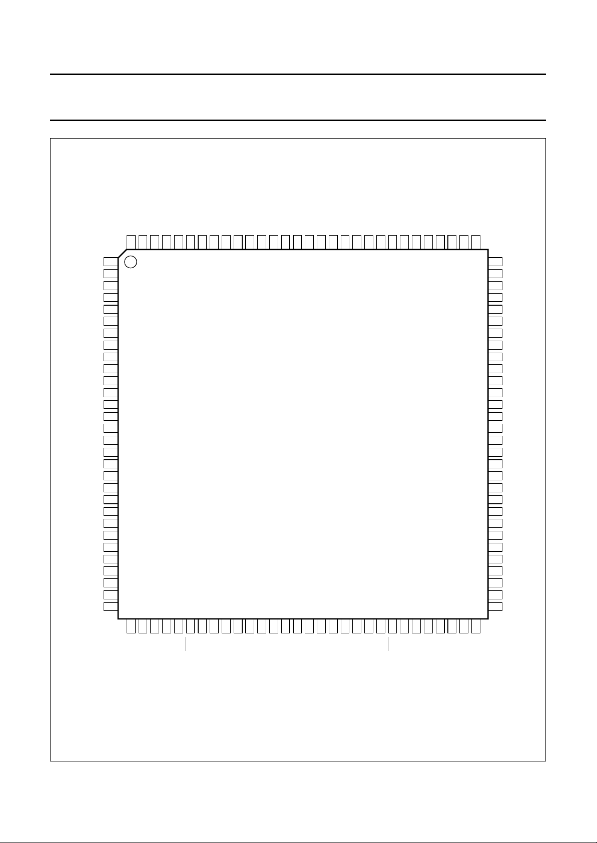
6 PINNING
SYMBOL PIN STATUS DESCRIPTION
XTAL 1 O 26.8 MHz crystal oscillator output, not used if TTL clock signal is used
XT ALI 2 I 26.8 MHz crystal oscillator input or external clock input (TTL, square wave)
2
SDA 3 I/O I
SCL 4 I I
2
CSA 5 I I2C-bus set address
I
CHR0 6 I digital chrominance input signal (bit 0)
CHR1 7 I digital chrominance input signal (bit 1)
CHR2 8 I digital chrominance input signal (bit 2)
CHR3 9 I digital chrominance input signal (bit 3)
CHR4 10 I digital chrominance input signal (bit 4)
CHR5 11 I digital chrominance input signal (bit 5)
CHR6 12 I digital chrominance input signal (bit 6)
CHR7 13 I digital chrominance input signal (bit 7)
V
DDD1
14 − +5 V digital supply voltage 1
CTST 15 − connected to ground (clock test pin)
V
SSD1
16 − digital ground 1 (0 V)
CVBS0 17 I digital CVBS input signal (bit 0)
CVBS1 18 I digital CVBS input signal (bit 1)
CVBS2 19 I digital CVBS input signal (bit 2)
CVBS3 20 I digital CVBS input signal (bit 3)
CVBS4 21 I digital CVBS input signal (bit 4)
CVBS5 22 I digital CVBS input signal (bit 5)
CVBS6 23 I digital CVBS input signal (bit 6)
CVBS7 24 I digital CVBS input signal (bit 7)
HSY 25 O horizontal sync indicator output (programmable)
HCL 26 O horizontal clamping pulse output (programmable)
V
DDA
27 − +5 V analog supply voltage
LFCO 28 O line frequency control output signal to CGC
V
V
V
SSA
SSD2
DDD2
29 − analog ground (0 V)
30 − digital ground 2 (0 V)
31 − +5 V digital supply voltage 2
GPSW2 32 O general purpose output 2 (controllable via I
GPSW1 33 O general purpose output 1 (controllable via I
RTS1 34 O real time status output1; controlled by bit RTSE
RTS0 35 O real time status output0; controlled by bit RTSE
RES 36 O reset output, active LOW
CGCE 37 I enable input for internal CGC (connected to +5 V)
CREF 38 O clock qualifier output (test only)
C-bus data line
2
C-bus clock line
(multiple of present line frequency)
2
C-bus)
2
C-bus)
1996 Nov 04 7
Philips Semiconductors Product specification
Digital video decoder, Scaler and Clock
SAA7196
generator circuit (DESCPro)
SYMBOL PIN STATUS DESCRIPTION
CREFB 39 I/O clock reference qualifier input/output (HIGH indicates valid data on
expansion port)
LLC 40 O line-locked video system clock output, for front-end (ADCs) only;
frequency: 1888 × f
for 60 Hz/525 lines per field systems
LLCB 41 I/O line-locked clock signal input/output, maximum 32 MHz (twice of pixel rate
in 4 : 2 : 2); frequency: 1888 × f
1560 × fH for 60 Hz/525 lines per field systems; or variable input clock up
to 32 MHz in input mode
LLC2 42 O line-locked clock signal output (pixel clock)
BTST 43 I connected to ground; BTST = HIGH sets all outputs (except
pins 1, 28, 38, 40 and 42) to high-impedance state (testing)
RTCO 44 O real time control output
V
DDD3
45 − +5 V digital supply voltage 3
VMUX 46 I VRAM output multiplexing, control input for the 32- to 16-bit multiplexer
(see Table 7)
V
SSD3
47 − digital ground 3 (0 V)
SODD 48 O odd/even field sequence reference output related to the scaler output
(test only)
SVS 49 O vertical sync signal related to the scaler output (test only)
SHREF 50 O delayed HREF signal related to the scaler output (test only)
PXQ 51 O pixel qualifier output signal to mark active pixels of a qualified line
(polarity: bit QPP; test only)
LNQ 52 O line qualifier output signal to mark active video phase
(polarity: bit QPP; test only)
VOE 53 I enable input of VRAM output
HFL 54 O FIFO half-full flag output signal
INCADR 55 O line increment/vertical reset control output
VCLK 56 I clock input signal of FIFO output
VRO31 57 O 32-bit digital VRAM output port (bit 31)
VRO30 58 O 32-bit digital VRAM output port (bit 30)
VRO29 59 O 32-bit digital VRAM output port (bit 29)
V
V
SSD4
DDD4
60 − digital ground 4 (0 V)
61 − +5 V digital supply voltage 4
VRO28 62 O 32-bit VRAM output port (bit 28)
VRO27 63 O 32-bit VRAM output port (bit 27)
VRO26 64 O 32-bit VRAM output port (bit 26)
VRO25 65 O 32-bit VRAM output port (bit 25)
VRO24 66 O 32-bit VRAM output port (bit 24)
VRO23 67 O 32-bit VRAM output port (bit 23)
VRO22 68 O 32-bit VRAM output port (bit 22)
VRO21 69 O 32-bit VRAM output port (bit 21)
VRO20 70 O 32-bit VRAM output port (bit 20)
for 50 Hz/625 lines per field systems and 1560 × f
H
for 50 Hz/625 lines per field systems and
H
H
1996 Nov 04 8
Philips Semiconductors Product specification
Digital video decoder, Scaler and Clock
SAA7196
generator circuit (DESCPro)
SYMBOL PIN STATUS DESCRIPTION
VRO19 71 O 32-bit VRAM output port (bit 19)
VRO18 72 O 32-bit VRAM output port (bit 18)
VRO17 73 O 32-bit VRAM output port (bit 17)
VRO16 74 O 32-bit VRAM output port (bit 16)
V
SSD5
i.c. 76 − internally connected
V
DDD5
VRO15 78 O 32-bit VRAM output port (bit 15)
VRO14 79 O 32-bit VRAM output port (bit 14)
VRO13 80 O 32-bit VRAM output port (bit 13)
VRO12 81 O 32-bit VRAM output port (bit 12)
VRO11 82 O 32-bit VRAM output port (bit 11)
VRO10 83 O 32-bit VRAM output port (bit 10)
VRO9 84 O 32-bit VRAM output port (bit 9)
VRO8 85 O 32-bit VRAM output port (bit 8)
VRO7 86 O 32-bit VRAM output port (bit 7)
VRO6 87 O 32-bit VRAM output port (bit 6)
VRO5 88 O 32-bit VRAM output port (bit 5)
VRO4 89 O 32-bit VRAM output port (bit 4)
VRO3 90 O 32-bit VRAM output port (bit 3)
V
DDD6
VRO2 92 O 32-bit VRAM output port (bit 2)
VRO1 93 O 32-bit VRAM output port (bit 1)
VRO0 94 O 32-bit VRAM output port (bit 0)
DIR 95 I direction control of expansion bus
YUV15 96 I/O digital 16-bit video input/output signal (bit 15); luminance (Y)
YUV14 97 I/O digital 16-bit video input/output signal (bit 14); luminance (Y)
YUV13 98 I/O digital 16-bit video input/output signal (bit 13); luminance (Y)
YUV12 99 I/O digital 16-bit video input/output signal (bit 12); luminance (Y)
YUV11 100 I/O digital 16-bit video input/output signal (bit 11); luminance (Y)
YUV10 101 I/O digital 16-bit video input/output signal (bit 10); luminance (Y)
YUV9 102 I/O digital 16-bit video input/output signal (bit 9); luminance (Y)
YUV8 103 I/O digital 16-bit video input/output signal (bit 8); luminance (Y)
V
SSD6
i.c. 105 − internally connected
V
DDD7
YUV7 107 I/O digital 16-bit video input/output signal (bit 7); colour difference signals (UV)
YUV6 108 I/O digital 16-bit video input/output signal (bit 6); colour difference signals (UV)
YUV5 109 I/O digital 16-bit video input/output signal (bit 5); colour difference signals (UV)
YUV4 110 I/O digital 16-bit video input/output signal (bit 4); colour difference signals (UV)
YUV3 111 I/O digital 16-bit video input/output signal (bit 3); colour difference signals (UV)
75 − digital ground 5 (0 V)
77 − +5 V digital supply voltage 5
91 − +5 V digital supply voltage 6
104 − digital ground 6 (0 V)
106 − +5 V digital supply voltage 7
1996 Nov 04 9
Philips Semiconductors Product specification
Digital video decoder, Scaler and Clock
SAA7196
generator circuit (DESCPro)
SYMBOL PIN STATUS DESCRIPTION
YUV2 112 I/O digital 16-bit video input/output signal (bit 2); colour difference signals (UV)
YUV1 113 I/O digital 16-bit video input/output signal (bit 1); colour difference signals (UV)
YUV0 114 I/O digital 16-bit video input/output signal (bit 0); colour difference signals (UV)
HREF 115 I/O horizontal reference signal
VS 116 I/O vertical sync input/output signal with respect to the YUV input signal
HS 117 O horizontal sync signal, programmable
AP 118 I connected to ground (action pin for testing)
SP 119 I connected to ground (shift pin for testing)
V
SSD7
120 − digital ground 7 (0 V)
1996 Nov 04 10
Philips Semiconductors Product specification
Digital video decoder, Scaler and Clock
generator circuit (DESCPro)
handbook, full pagewidth
XTAL
XTALI
SDA
SCL
I2CSA
CHR0
CHR1
CHR2
CHR3
CHR4
CHR5
CHR6
CHR7
V
DDD1
CTST
V
SSD1
CVBS0
CVBS1
CVBS2
CVBS3
CVBS4
CVBS5
CVBS6
CVBS7
HSY
HCL
V
DDA
LFCO
V
SSA
V
SSD2
SSD7
V
120
1
2
3
4
5
6
7
8
9
10
11
12
13
14
15
16
17
18
19
20
21
22
23
24
25
26
27
28
29
30
SP
119
AP
118
HS
117
VS
116
HREF
115
YUV0
114
YUV1
113
YUV2
112
YUV3
111
YUV4
110
YUV5
109
YUV6
108
SAA7196
YUV7
107
DDD7
V
106
i.c.
105
SSD6
V
104
YUV8
103
YUV9
102
YUV15
YUV14
YUV13
YUV12
YUV11
YUV10
999897969594939291
101
100
DIR
VRO0
SAA7196
DDD6
VRO2
VRO1
V
90
89
88
87
86
85
84
83
82
81
80
79
78
77
76
75
74
73
72
71
70
69
68
67
66
65
64
63
62
61
VRO3
VRO4
VRO5
VRO6
VRO7
VRO8
VRO9
VRO10
VRO11
VRO12
VRO13
VRO14
VRO15
V
DDD5
i.c.
V
SSD5
VRO16
VRO17
VRO18
VRO19
VRO20
VRO21
VRO22
VRO23
VRO24
VRO25
VRO26
VRO27
VRO28
V
DDD4
3132333435363738394041424344454647484950515253545556575859
DDD2
V
GPSW2
GPSW1
RTS1
RTS0
RES
CGCE
CREF
LLC
CREFB
LLCB
LLC2
BTST
RTCO
Fig.3 Pin configuration.
1996 Nov 04 11
DDD3
V
VMUX
V
SSD3
SVS
SODD
PXQ
SHREF
LNQ
VOE
HFL
VCLK
INCADR
VRO31
VRO30
60
SSD4
VRO29
V
MHA379

Philips Semiconductors Product specification
Digital video decoder, Scaler and Clock
generator circuit (DESCPro)
7 FUNCTIONAL DESCRIPTION
7.1 Decoder part
PAL, NTSC and SECAM standard colour signals based on
line-locked clock are decoded (see Fig.27). In Y/C mode,
digitized luminance CVBS7 to CVBS0 and chrominance
CHR7 to CHR0 signals (digitized in two external ADCs)
are input. In normal mode only CVBS7 to CVBS0 is used.
The data rate is 29.5 MHz (50 MHz systems) or
24.54 MHz (60 MHz systems).
7.1.1 C
The input signal passes the input interface and the
chrominance band-pass filter to eliminate DC components
and is finally fed to the multiplicative inputs of a quadrature
demodulator, where two subcarrier signals (0 and 90°
phase-shifted) from a local digital oscillator (DTO1) are
applied.
The frequency is dependent on the present colour
standard. The signals are low-pass filtered and amplified
in a gain-controlled amplifier. A final low-pass stage
provides a correct bandwidth performance.
PAL signals are comb-filtered to eliminate crosstalk
between the chrominance channels according to PAL
standard requirements.
NTSC signals are comb-filtered to eliminate crosstalk from
luminance to chrominance for vertical structures.
SECAM signals are fed through a cloche filter, a phase
demodulator and a differentiator to achieve proportionality
to the instantaneous frequency. The signals are
de-multiplexed in the SECAM recombination stage after
passing a de-emphasis stage to provide the two serially
transmitted colour difference signals.
The PLL for quadrature demodulation is closed via the
cloche filter (to improve noise performance), a phase
demodulator, a burst gate accumulator, a loop filter PI1
and a discrete time oscillator DTO1. The gain control loop
is closed via the cloche filter, amplitude detector, a burst
gate accumulator and a loop filter PI2.
The sequence processor switches signals according to
standards.
7.1.2 L
The data rate of the input signal is reduced to LLC2
frequency by a sample rate converter in the input interface.
The high frequency components are emphasized in a
prefilter to compensate for losses in the succeeding
chrominance trap. The chrominance trap is adjusted to a
HROMINANCE PROCESSOR
UMINANCE PROCESSOR
SAA7196
centre frequency of 3.58 MHz (NTSC) or 4.4 MHz (PAL,
SECAM) to eliminate most of the colour carrier
components. The chrominance trap is bypassed for
S-VHS signals.
The high frequency components in the luminance signal
are ‘peaked’ using a band-pass filter and a coring stage.
The ‘peaked’ (high frequent) component is added to the
‘unpeaked’ signal part for sharpness improvement and
output via variable delay to the expansion bus.
7.1.3 S
The sync input signal is reduced in bandwidth to 1 MHz
before it is sliced and separated from the luminance signal.
The sync pulses are compared in a detector with the
divided clock signal of a counter. The resulting output
signal is fed to a loop filter that accumulates all the phase
deviations. Thereby, a discrete time oscillator DTO2 is
driven generating the line frequency control signal LFCO.
An external PLL generates the line-locked clock LLC from
the signal LFCO. A noise-limited vertical deflection pulse is
generated for vertical processing that also inserts artificial
pulses if vertical input pulses are missing. 50/60 Hz as well
as odd/even field is automatically detected by the
identification stage.
7.2 Expansion port
The expansion port is a bidirectional interface for digital
video signals YUV15 to YUV0 in 4:2:2 format (see
Table 5). External video signals can be inserted to the
scaler or decoded video signals of the decoder part can be
output.
The data direction is controlled by pin 95 (DIR = HIGH:
data from external; see Table 4).
YUV15 to YUV0, HREF, VS, LLCB and CREFB pins are
inputs when bits OECL, OEHV, OEYC of subaddress 0E
are set to ‘0’. Different modes are provided (for timing see
Figs 6 to 8):
• Mode 0: all bidirectional terminals are outputs.
The signal of the decoder part (internal YUV15 to YUV0)
is switched to be scaled.
• Mode 1: external YUV15 to YUV0 is input to the scaler.
LLCB/CREFB clock system and HREF/VS from the
SAA7196 are used to control the external source. It is
possible to switch between mode 0 and mode 1 by
means of DIR input (see Fig.5).
• Mode 2: External YUV15 to YUV0 is input to the scaler.
LLCB/ CREFB clock system and HREF/VS from
external are used.
YNCHRONIZATION
1996 Nov 04 12
Philips Semiconductors Product specification
Digital video decoder, Scaler and Clock
generator circuit (DESCPro)
• Mode 3: YUV15 to YUV0 and HREF/VS terminals are
inputs. External YUV15 to YUV0 is input to the scaler
with HREF/VS reference from external. LLCB/CREFB
clock system of the SAA7196 is used.
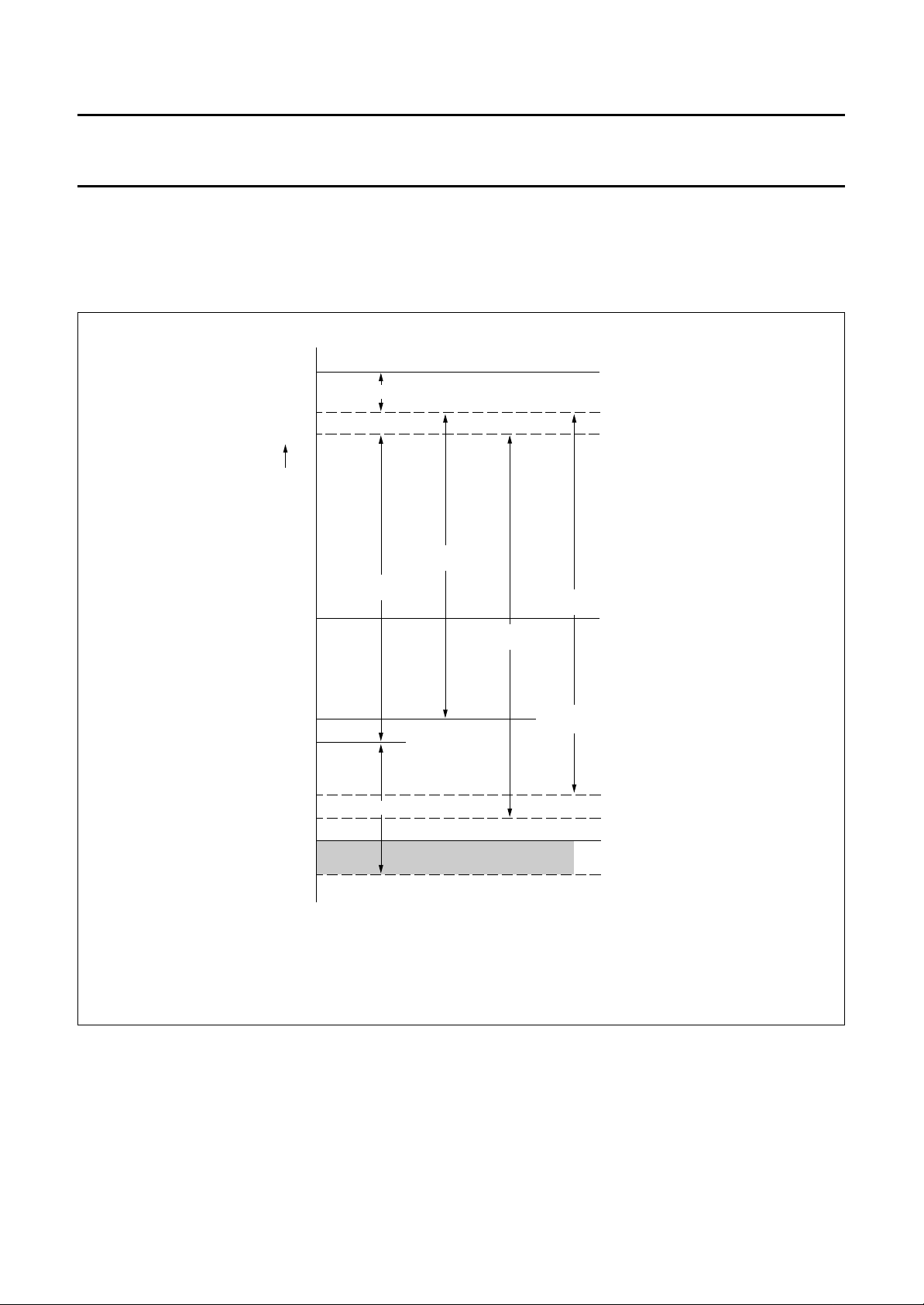
handbook, full pagewidth
+127
reserved
+106
+95
digital
signal
value
luminance
60 Hz mode
luminance
50 Hz mode
0
SAA7196
pixel wise switching of the scaler source is possible
because the internal clock and sync sources are used.
100% white (60 Hz mode)
100% white (50 Hz mode)
chrominance
60 Hz mode
chrominance
50 Hz mode
−52
−64
−91
−103
−128
−132
All levels are related to EBU colour bar. Values in
decimal at 100% luminance and 75%chrominance
amplitude.
Fig.4 CVBS7 to CVBS0 input signal ranges.
black (60 Hz mode)
= black (50 Hz mode)
blanking level
sync
clipped
MHA380
1996 Nov 04 13
Philips Semiconductors Product specification
Digital video decoder, Scaler and Clock
generator circuit (DESCPro)
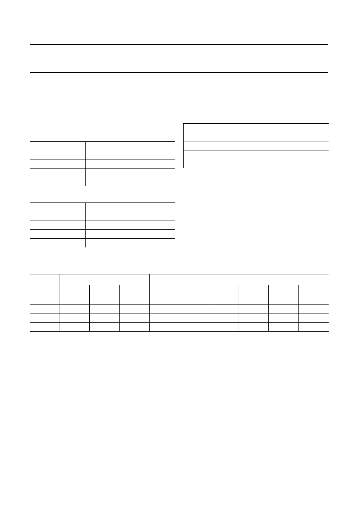
7.3 Monitor controls BCS
7.3.1 B
The luminance signal can be controlled via I2C-bus
(see Table 16) by the bits BRIG7 to BRIG0 and
CONT6 to CONT0.
Table 1 Brightness control
00H minimum offset
80H CCIR level
FFH maximum offset
Table 2 Contrast control
00H luminance off
40H CCIR level
7FH 1.9999 amplitude
RIGHTNESS AND CONTRAST CONTROLS
BRIGHTNESS
CONTROL
CONTRAST
CONTROL
VALUE
VALUE
SAA7196
7.3.2 SATURATION CONTROL
The chrominance signal can be controlled via I2C-bus (see
Table 16) by the bits SAT6 to SAT0 and HUE7 to HUE0.
Table 3 Saturation control
SATURATION
CONTROL
00H colour off
40H CCIR level
7FH 1.9999 amplitude
Clipping: all resulting output values are clipped to
minimum (equals 1) and maximum (equals 254).
VALUE
Table 4 Operation modes; notes 1 to 3
MODE
OEYC OEHV OECL PIN 95 YUV HREF VS LLCB CREFB
0111LOWOOOOO
1 X 1 1 HIGH I OOOO
2 X 0 0 HIGH IIIII
3 X 0 1 HIGH I I I O O
Notes
1. X = don’t care.
2. I = input to monitor control/scaler.
3. O = output from decoder.
I2C BIT DIR INPUT SOURCE
1996 Nov 04 14
Philips Semiconductors Product specification
Digital video decoder, Scaler and Clock
generator circuit (DESCPro)
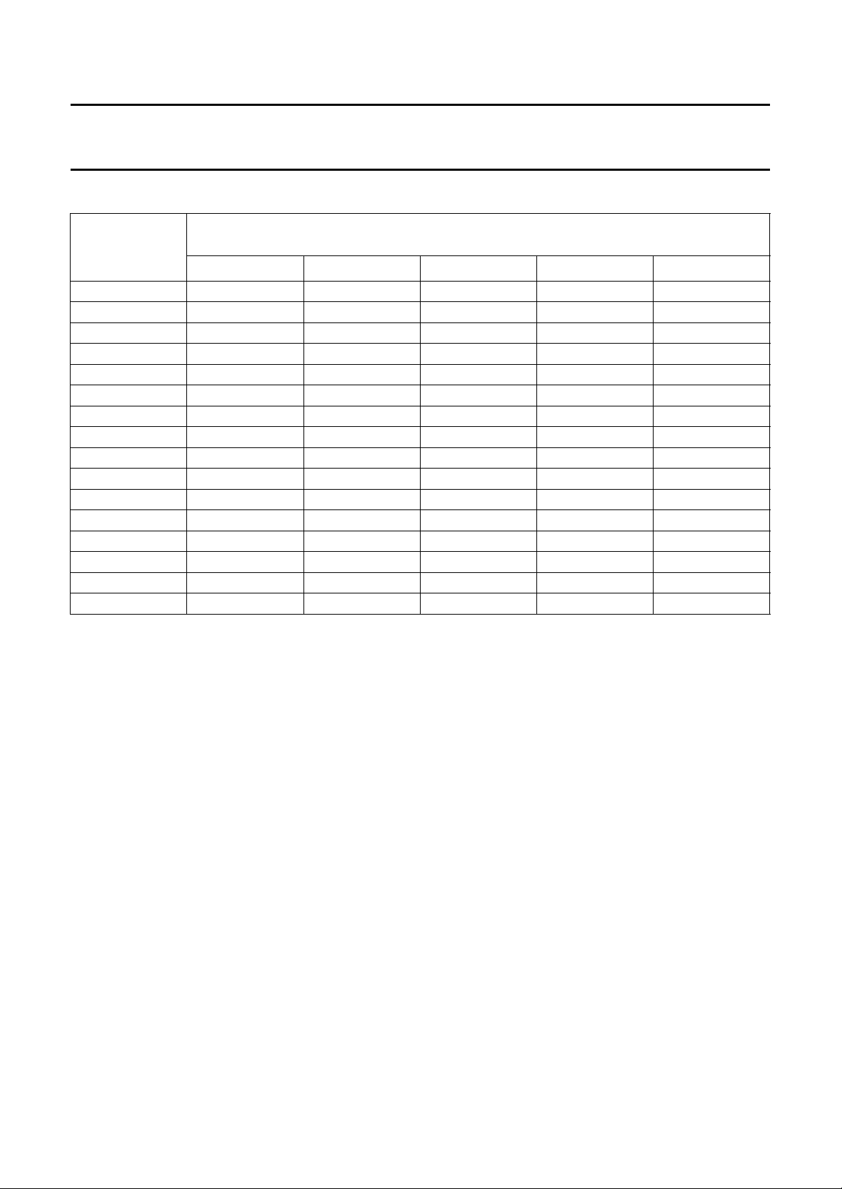
Table 5 YUV-bus format on expansion port; note 1
SIGNALS ON EXPANSION PORT (PIXEL BYTE SEQUENCE ON PINS)
PIN
n n+1 n+2 n+3 n+4
YUV15 Ye7 Yo7 Ye7 Yo7 Ye7
YUV14 Ye6 Yo6 Ye6 Yo6 Ye6
YUV13 Ye5 Yo5 Ye5 Yo5 Ye5
YUV12 Ye4 Yo4 Ye4 Yo4 Ye4
YUV11 Ye3 Yo3 Ye3 Yo3 Ye3
YUV10 Ye2 Yo2 Ye2 Yo2 Ye2
YUV9 Ye1 Yo1 Ye1 Yo1 Ye1
YUV8 Ye0 Yo0 Ye0 Yo0 Ye0
YUV7 Ue7 Ve7 Ue7 Ve7 Ue7
YUV6 Ue6 Ve6 Ue6 Ve6 Ue6
YUV5 Ue5 Ve5 Ue5 Ve5 Ue5
YUV4 Ue4 Ve4 Ue4 Ve4 Ue4
YUV3 Ue3 Ve3 Ue3 Ve3 Ue3
YUV2 Ue2 Ve2 Ue2 Ve2 Ue2
YUV1 Ue1 Ve1 Ue1 Ve1 Ue1
YUV0 Ue0 Ve0 Ue0 Ve0 Ue0
PIXEL ORDER
SAA7196
Note
1. e = even pixel number; o = odd pixel number.
1996 Nov 04 15
Philips Semiconductors Product specification
Digital video decoder, Scaler and Clock
generator circuit (DESCPro)
handbook, full pagewidth
LLCB
CREFB
HREF
DIR
UV
dec
(from decoder)
UV
ext
(from external
port)
UV to scaler
U
0(dec)
U
0(dec)
t
to 3-state
t
SU
t
OH
V
V
0(dec)
0(dec)
t
PZ
t
U
U
HD
2(ext)
2(ext)
t
from 3-state
V
2(ext)
V
2(ext)
U
4(dec)
U
4(dec)
SAA7196
V
4(dec)
V
4(dec)
MHA383
t
from 3-state(min)
t
from 3-state>tto 3-state
t
to 3-state(max)
= 1.5LLC + t
= 1.5LLC + t
Fig.5 Real-time switching between mode 0 and mode 1 (internal/external YUV15 to YUV0).
PZ(min)
PZ(max)
1996 Nov 04 16
Philips Semiconductors Product specification
Digital video decoder, Scaler and Clock
generator circuit (DESCPro)
handbook, full pagewidth
input CVBS
HREF
VS
ODD (RTSO)
1625 23456
SAA7196
789
540 × 2/LLC
1 × 2/LLC
MHA384
handbook, full pagewidth
input CVBS
HREF
VS
ODD (RTSO)
a. 1st field.
314313 315 316 317 318 319
b. 2nd field
320 321
68 × 2/LLC
1 × 2/LLC
MHA385
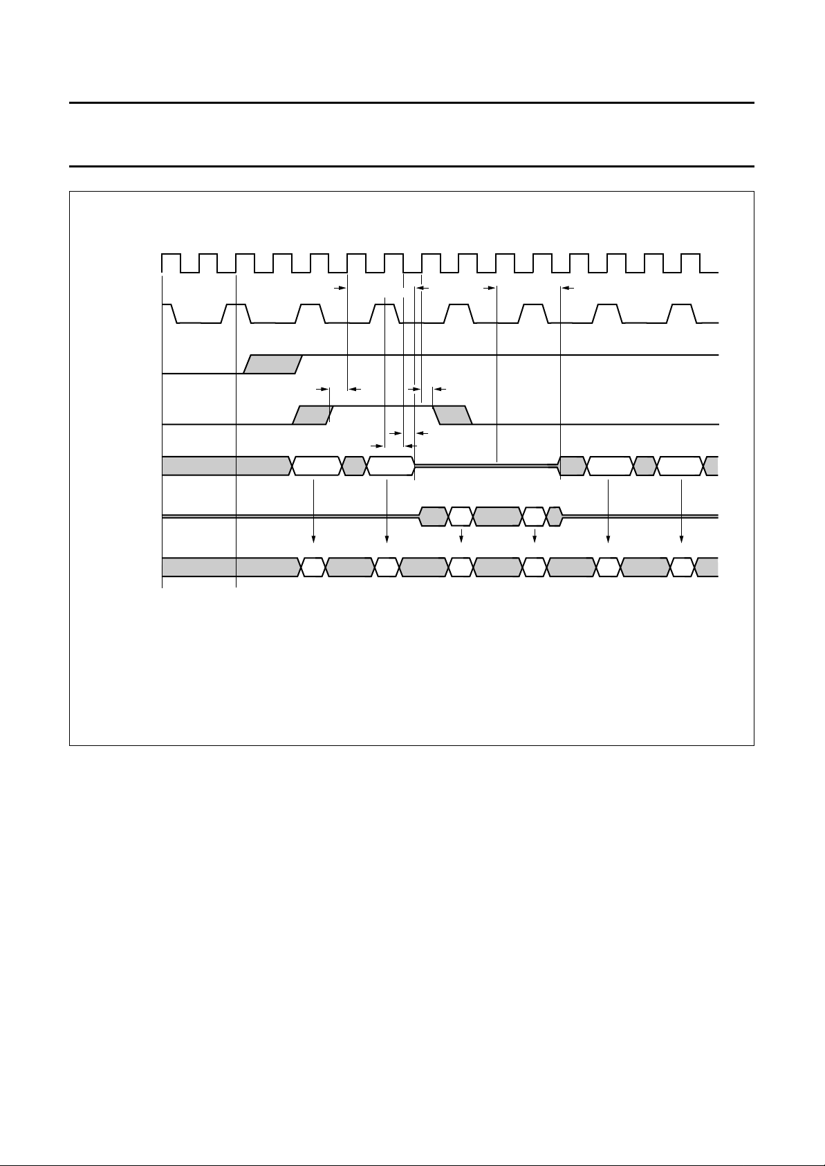
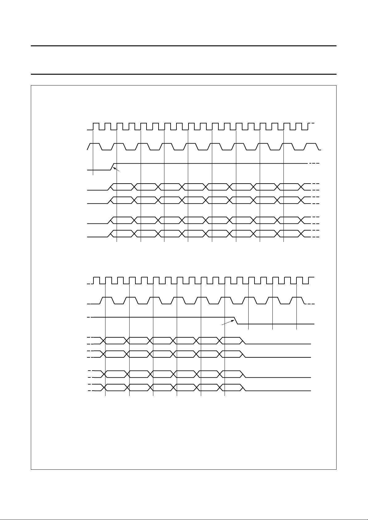
Fig.6 VS and ODD timing on expansion port (50 Hz).
1996 Nov 04 17
Philips Semiconductors Product specification
Digital video decoder, Scaler and Clock
generator circuit (DESCPro)
handbook, full pagewidth
input CVBS
HREF
VS
ODD (RTSO)
1525 2 3 4 5 6
a. 1st field.
SAA7196
78
448 × 2/LLC
1 × 2/LLC
9
MHA386
handbook, full pagewidth
input CVBS
HREF
VS
ODD (RTSO)
263 264 265 266 267 268
b. 2nd field.
269 270 271
58 × 2/LLC
1 × 2/LLC
MHA387
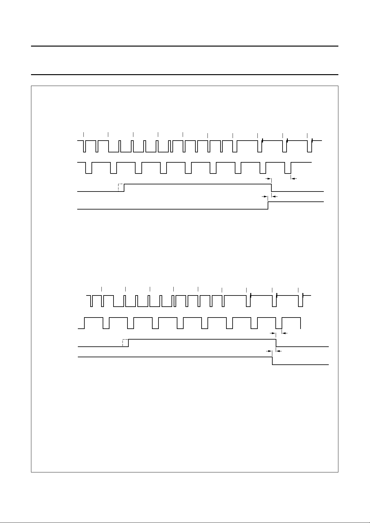
Fig.7 VS and ODD timing on expansion port (60 Hz).
1996 Nov 04 18
Philips Semiconductors Product specification
Digital video decoder, Scaler and Clock
generator circuit (DESCPro)
handbook, full pagewidth
programming range
(step size: 2/LLC)
programming range
(step size: 2/LLC)
CVBS
HSY
HSY
HCL
HCL
62 × 2/LLC
(1)
+191
(1)
+127
216 LLC
processing delay CVBS - YUV
at YDEL = 000b
0
0
0
SAA7196
burst
−64
−128
10 × 2/LLC
Y−output
HREF (50 Hz)
PLIN (RTS1)
(50 Hz only)
HS (50 Hz)
HS (50 Hz)
programming range
(step size: 8/LLC)
HREF (60 Hz)
HS (60 Hz)
HS (60 Hz)
programming range
(step size: 8/LLC)
(2)
(2)
+117
+97
768 × 2/LLC
36 × 2/LLC
640 × 2/LLC
176 × 2/LLC
104 × 2/LLC
64 × 2/LLC
0
36 × 2/LLC
140 × 2/LLC
64 × 2/LLC
0
2 × 2/LLC
−118
−97
MHA388
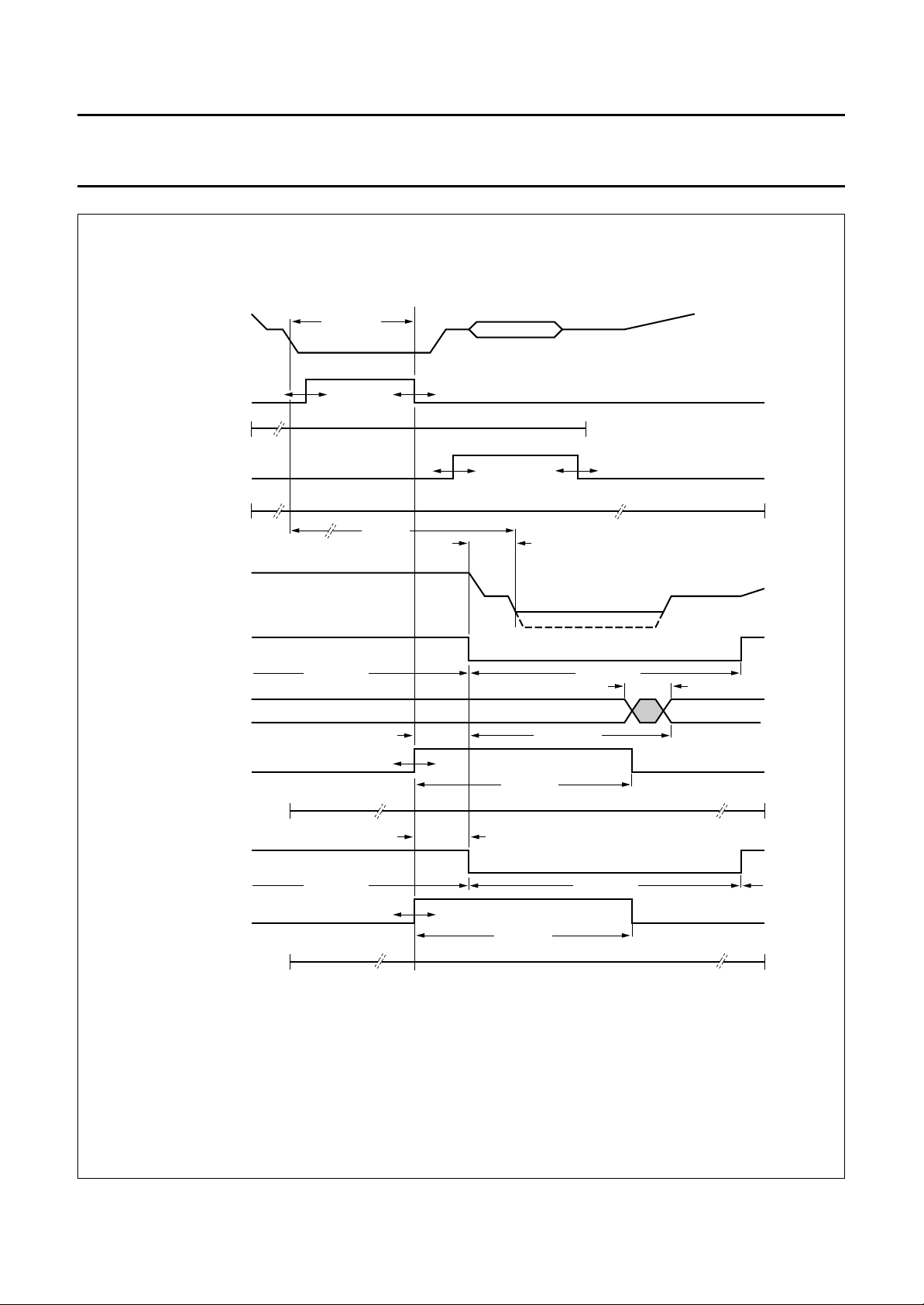
Fig.8 Horizontal sync timing at HRMV = 0 and HRFS = 0 (signals HSY, HCL, HREF, PLIN and HS; 50 and 60 Hz).
1996 Nov 04 19
Philips Semiconductors Product specification
Digital video decoder, Scaler and Clock
generator circuit (DESCPro)
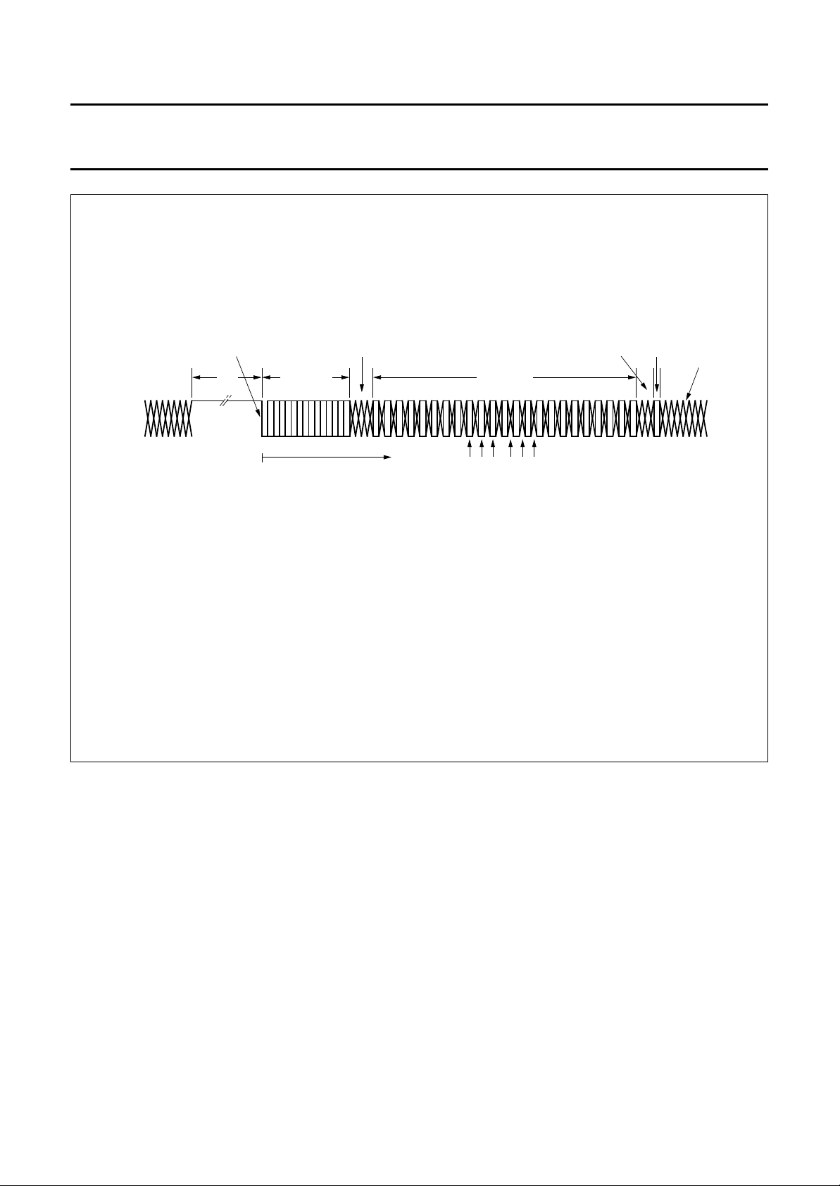
ndbook, full pagewidth
LLCB
CREFB
HREF
Byte numbers for pixels:
Y signal
50 Hz
U and V signal
Y signal
60 Hz
U and V signal
start of
active line
0
U0
0
U0
V0
V0
1
1
2
U2
2
U2
V2
V2
SAA7196
U4
U4
4
4
5
V4
5
V4
U6
U6
6
6
7
V6
7
V6
3
3
LLCB
CREFB
HREF
Byte numbers for pixels:
Y signal
50 Hz
U and V signal
Y signal
60 Hz
U and V signal
762
U762
634
U634
763
V762
635
V634
764
U764
636
U636
765
V764
637
V636
end of
active line
766
U766
638
U638
767
V766
639
V638
MHA389
Fig.9 Horizontal and data multiplex timing on expansion port.
1996 Nov 04 20
Philips Semiconductors Product specification
Digital video decoder, Scaler and Clock
generator circuit (DESCPro)
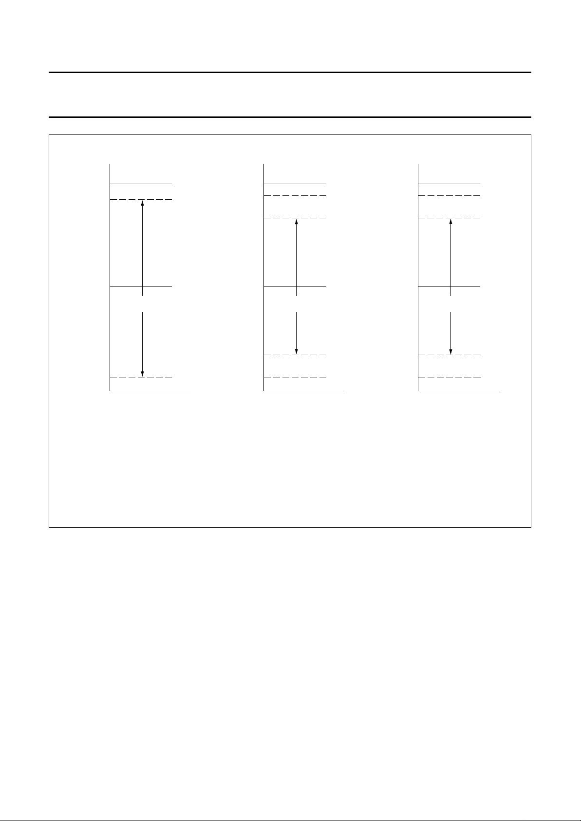
handbook, full pagewidth
digital
signal
value
+254
+235
+128
white 100%
luminance
levels
digital
signal
value
+254
+240
+212
+128
+44
U-component
levels
blue 100%
blue 75%
yellow 75%
digital
signal
value
+254
+240
+212
+128
+44
SAA7196
red 100%
red 75%
V-component
levels
cyan 75%
+16
1
black yellow 100%
+16
1
b. U signal range (B − Y). c. V signal range (R − Y).a. Y signal range.
Fig.10 Input and output signal levels on expansion port.
7.3.3 RTCO OUTPUT PIN 44
This real-time control and status output signal contains
serial information about actual system clock, subcarrier
frequency and PAL/SECAM sequence (see Fig.11).
The signal can be used for various applications in external
circuits, e.g. in a digital encoder to achieve ‘clean’
encoding.
+16
1
cyan 100%
MHA390
7.3.4 RTS1 AND RTS0 OUTPUTS (PINS 34 AND 35)
These outputs can be configured in two modes dependent
on bit RTSE (subaddress 0D):
• RTSE = 0: the output RTS0 contains the odd/even field
identification bit (HIGH equals odd); output RTS1
contains the inverted PAL/SECAM sequence bit [HIGH
equals non-inverted (R − Y)-line/DB-line]
• RTSE = 1: the output RTS0 contains the horizontal lock
bit (HIGH equals PLL locked); output RTS1 contains the
vertical detection bit (HIGH equals vertical sync
detected).
1996 Nov 04 21
Philips Semiconductors Product specification
Digital video decoder, Scaler and Clock
generator circuit (DESCPro)
handbook, full pagewidth
RTCO
H/L transition
(counter start)
128
clock cycles
4 bits
HPLL
increment
bits 13 to 0
13
048 1419 6367
reserve
022201510 51
time slot
(LLC/4)
FSCPLL increment
bits 22 to 0
valid
not valid
3 bits
reserve
sequence
bit (1)
0
SAA7196
reserved (2)
MHA391
(1) Sequence bit:
SECAM: 0 equals DB-line; 1 equals DR-line.
PAL: 0 equals (R − Y) line normal; 1 equals (R − Y) line inverted.
NTSC: 0 (no change).
(2) Reserve bits: 276 for 50 Hz systems; 188 for 60 Hz systems.
Fig.11 RTCO timing.
7.4 Scaler part
The scaler part receives YUV15 to YUV0 input data in
4:2:2 format.
The video data from the BCS control are processed in
horizontal direction in two separate decimation filters.
The luminance component is also processed in vertical
direction (VPU_Y).
Chrominance data are interpolated to a 4 : 4 : 4 format;
a chroma keying bit is generated. The 4 :4:4 YUV data
are then converted from the YUV to the RGB domain in a
digital matrix. ROM tables in the RGB data path can be
used for anti-gamma correction of gamma-corrected input
signals. Uncorrected RGB and YUV signals can be
bypassed.
A scale control unit generates reference and gate signals
for scaling of the processed video data. After data
formatting to the various VRAM port formats, the scaled
video data are buffered in the 16 word 32-bit output FIFO
register. The scaling is performed by pixel and line
dropping at the FIFO input. The FIFO output is directly
connected to the VRAM output bus VRO31 to VRO0.
Specific reference signals support an easy memory
interfacing.
1996 Nov 04 22

Philips Semiconductors Product specification
Digital video decoder, Scaler and Clock
generator circuit (DESCPro)
7.4.1 DECIMATION FILTERS
The decimation filters perform accurate horizontal filtering
of the input data stream.
The signal bandwidth is matched in front of the pixel
decimation stage, thus disturbing artifacts, caused by the
pixel dropping, are reduced.
The signal bandwidth can be reduced in steps of
(see Figs 29 and 30):
2-tap filter = −6 dB at 0.325 pixel rate
3-tap filter = −6 dB at 0.25 pixel rate
4-tap filter = −6 dB at 0.21 pixel rate
5-tap filter = −6 dB at 0.125 pixel rate
9-tap filter = −6 dB at 0.075 pixel rate.
The different characteristics are chosen independently by
2
C-bus control bits HF2 to HF0 when AFS = 0
I
(subaddress 28). In the adaptive mode with AFS = 1,
the filter characteristics are chosen dependent on the
defined sizing parameters (see Table 6).
SAA7196
7.4.3 RGB MATRIX
Y data and UV data are converted after interpolation into
RGB data according to CCIR601 recommendation. Data is
bypassed in 16-bit YUV formats or monochrome modes.
The matrix equations are these considering the digital
quantization:
R = Y + 1.375 V
G=Y−0.703125 V − 0.34375 U
B = Y + 1.734375 U.
7.4.3.1 Anti-gamma ROM tables
ROM tables are implemented at the matrix output to
provide anti-gamma correction of the RGB data. A curve
for a gamma of 1.4 is implemented. The tables can be
used (bit RTB = 0, subaddress 20) to compensate gamma
correction for linear data representation of RGB output
data.
7.4.4 C
HROMINANCE SIGNAL KEYER
7.4.2 V
Luminance data is fed to a vertical filter consisting of a
384 × 8-bit RAM and an arithmetic block (see Fig.2).
Subsampled and interpolation operations are applied.
The luminance data is processed in vertical direction to
preserve the video information for small scaling factors
and to reduce artifacts caused by the dropping.
The available modes respectively transfer functions are
selectable by bits VP1 and VP0 (subaddress 28).
Adaptive modes, controlled by AFS and AFG bits
(subaddresses 28 and 30) are also available (see
Table 6).
Table 6 Adaptive filter selection (AFS = 1)
SCALING RATIO FILTER FUNCTION
XD/XS horizontal
≤1 bypassed
≤14/15 filter 1
≤11/15 filter 6
≤7/15 filter 3
≤3/15 filter 4
YD/YS vertical
≤1 bypassed
≤13/15 filter 1
≤4/15 filter 2
ERTICAL PROCESSING (VPU_Y)
(1)
The keyer generates an alpha signal to achieve a 5-5-5+α
RGB alpha output signal. Therefore, the processed UV
data amplitudes are compared with thresholds set via
I2C-bus (subaddresses ‘2C to 2F’). A logic ‘1’ signal is
generated if the amplitude is inside the specified amplitude
range, otherwise a logic ‘0’ is generated.
Keying can be switched off by setting the lower limit higher
than the upper limit (‘2C or 2E’ and ‘2D or 2F’).
7.4.5 S
The scale control block SC includes address/sequence
counters to define the current position in the input field and
to address the internal VPU memories. To perform scaling,
XD of XS pixel selection in horizontal direction and YD of
YS line selection in vertical direction are applied. The pixel
and line dropping are controlled at the input of the FIFO
register.
The scaling ratio in horizontal and vertical direction is
estimated to control the decimation filter function and the
vertical data processing in the adaptive mode (AFS and
AFG bits). The input field can be divided into two vertical
regions - the bypass region and the scaling region, which
are defined via I2C-bus by the parameters VS, VC, YO and
YS.
CALE CONTROL AND VERTICAL REGIONS
Note
1. See Chapter 8.
1996 Nov 04 23
 Loading...