

Philips saa7188a DATASHEETS
INTEGRATED CIRCUITS
DATA SH EET
SAA7188A
Digital Video Encoder (DENC2-M)
Preliminary specification
Supersedes data of 1995 Sep 21
File under Integrated Circuits, IC22
1996 Jul 08
Philips Semiconductors Preliminary specification
Digital Video Encoder (DENC2-M) SAA7188A
FEATURES
• CMOS 5 V device
• Digital PAL/NTSC encoder
• System pixel frequency 13.5 MHz
• Accepts MPEG decoded data
• 8-bit wide MPEG port
• Input data format Cb, Y, Cr, etc. (CCIR 656)
• 16-bit wide YUV input port
• I2C-bus control port or alternatively MPU parallel
control port
• Encoder can be master or slave
• Programmable horizontal and vertical input
synchronization phase
• Programmable horizontal sync output phase
• OSD overlay with Look-Up Tables (LUTs) 8 × 3 bytes
• Colour bar generator
• Line 21 Closed Caption encoder
• Macrovision Pay-per-View copy protection system as
option
The device is protected by USA patent numbers
4631603, 4577216 and 4819098 and other intellectual
property rights. Use of the Macrovision anti-copy
process in the device is licensed for non-commercial
home use only, which is its sole intended use in
this device.
Please contact your nearest Philips Semiconductors
sales office for more information.
• Cross-colour reduction
• DACs operating at 27 MHz with 10-bit resolution
• Controlled rise/fall times of output syncs and blanking
• Down-mode of DACs
• CVBS and S-Video output simultaneously
• PLCC68 package.
GENERAL DESCRIPTION
The SAA7188A encodes digital YUV video data to an
NTSC, PAL CVBS or S-Video signal.
The circuit accepts CCIR compatible YUV data with
720 active pixels per line in 4:2:2 multiplexed formats,
e.g. MPEG decoded data. It includes a sync/clock
generator and on-chip Digital-to-Analog Converters
(DACs).
The circuit is compatible to the DIG-TV2 chip family.
QUICK REFERENCE DATA
SYMBOL PARAMETER MIN. TYP. MAX. UNIT
V
V
I
DDA
I
DDD
V
V
DDA
DDD
i
o(p-p)
analog supply voltage 4.75 5.0 5.25 V
digital supply voltage 4.5 5.0 5.5 V
analog supply current − 50 55 mA
digital supply current − 140 170 mA
input signal voltage levels TTL compatible
analog output signal voltages Y, C and CVBS without load
− 2 − V
(peak-to-peak value)
R
L
load resistance 80 −−Ω
ILE LF integral linearity error −−±2 LSB
DLE LF differential linearity error −−±1 LSB
T
amb
operating ambient temperature 0 − +70 °C
1996 Jul 08 2
Philips Semiconductors Preliminary specification
Digital Video Encoder (DENC2-M) SAA7188A
ORDERING INFORMATION
TYPE NUMBER
PACKAGE
NAME DESCRIPTION VERSION
SAA7188AWP PLCC68 plastic leaded chip carrier; 68 leads SOT188-2
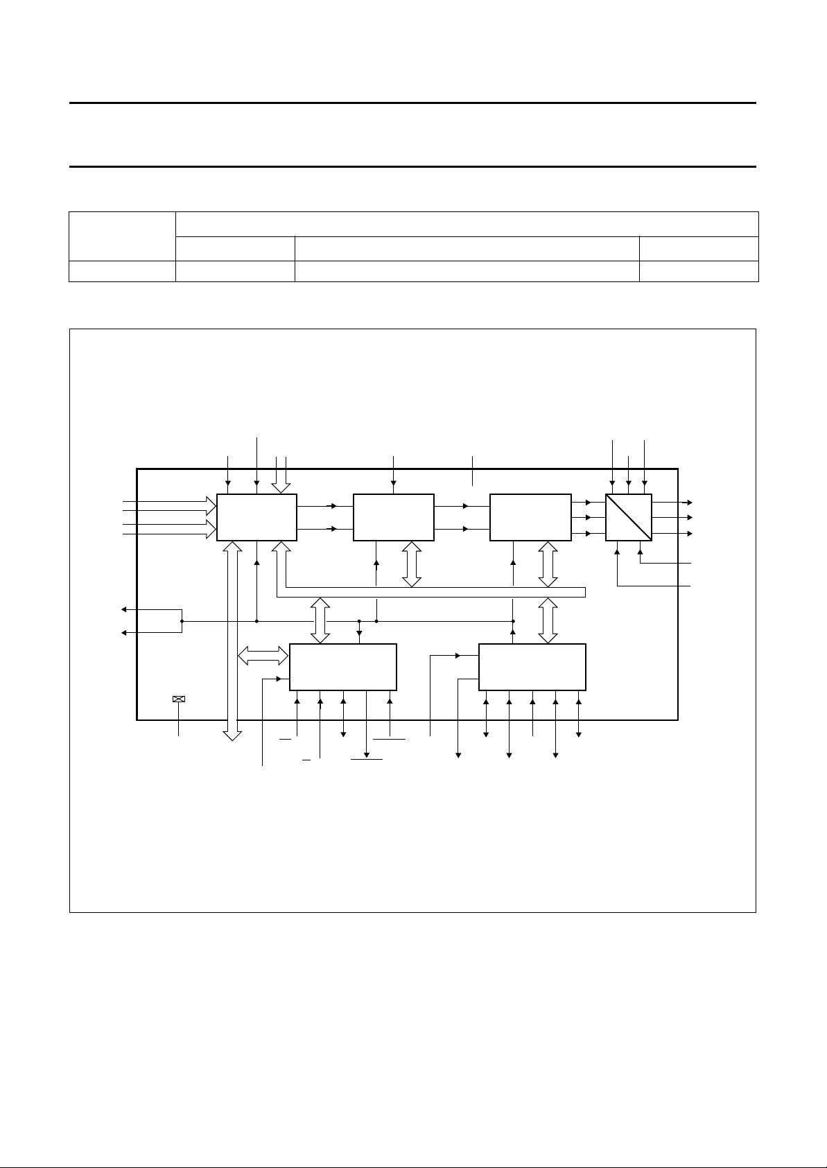
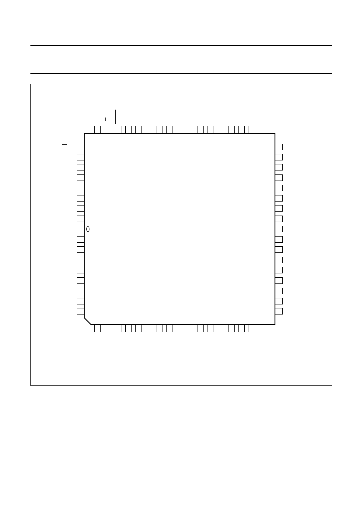
BLOCK DIAGRAM
V
DDA1
refH
to
V
DDA4
I
I
48,50,
5547
54,56
53
51
49
52
46
CVBS
Y
CHROMA
V
SSA
V
refL
A
D
MBG266
MP7
to MP0
VP0
to VP7
RCM1
RCM2
20 to 27
9 to 16
29
30
1,8,19
28,35,
42,62
V
SSD1
V
SSD7
to
SEL_ED
8
8
63 to 66
2 to 5
18
MANAGER
8
DP0
to DP7
SEL_MPU
KEY
DATA
OSD0
to OSD2
31
8
CS/SA
V
DDD1
RTCI
32 to 34
8
CONTROL
INTERFACE
6168
59 60 58 57 41 40 38 39 36 6 7
A0/SDA
RW/SCL
DTACK
43
ENCODER
88
clock timing signals
RESET
to V
DDD3
17,37,67
internal control bus
XTALI
LLC
XTALO
INTERFACE
CREF
OUTPUT
SYNC
CLK
CDIR
8
RCV1
V
SAA7188A
RCV2
Fig.1 Block diagram.
1996 Jul 08 3
k, full pagewidth
Philips Semiconductors Preliminary specification
Digital Video Encoder (DENC2-M) SAA7188A
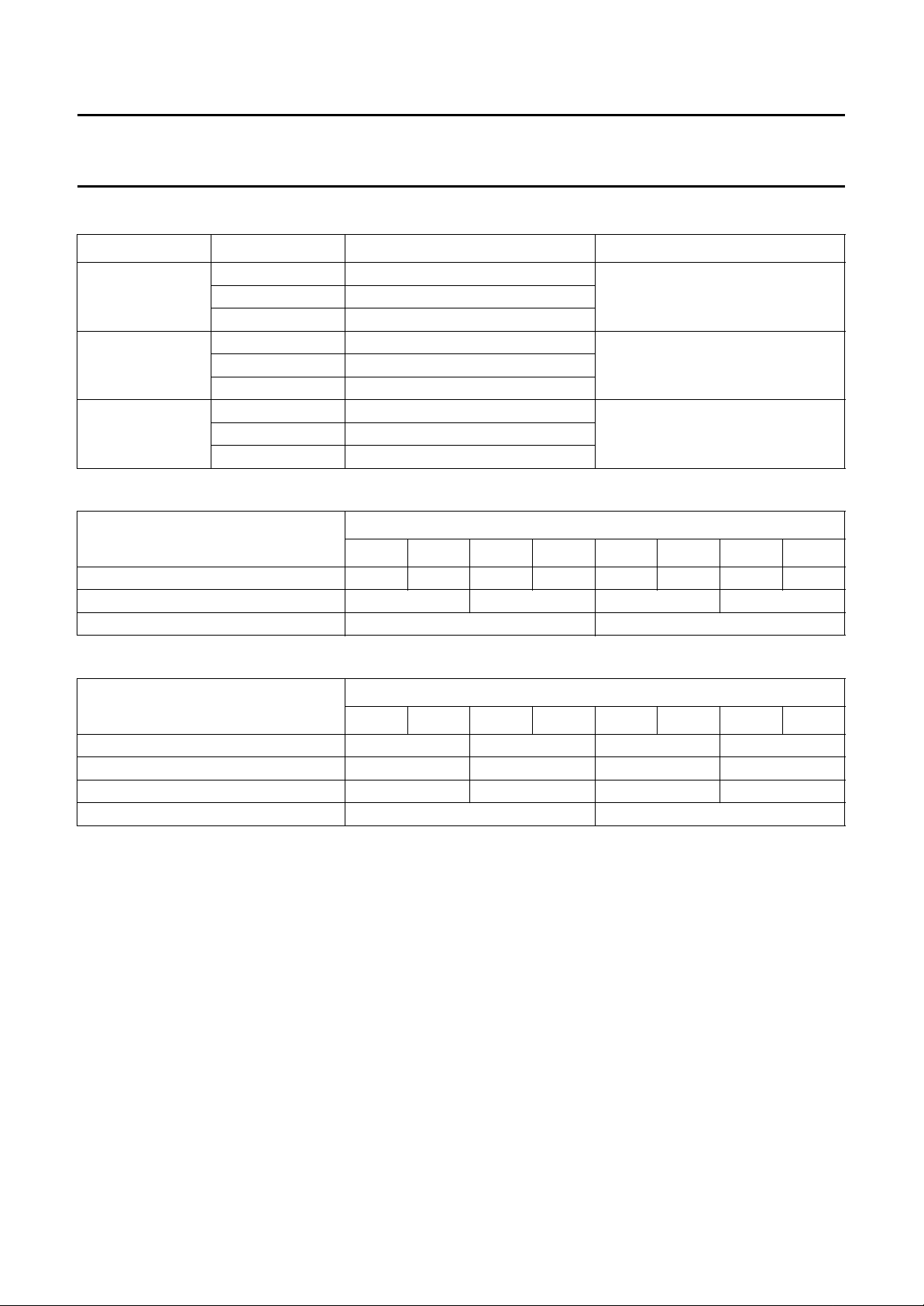
PINNING
SYMBOL PIN DESCRIPTION
V
SSD1
DP4 2
DP5 3
DP6 4
DP7 5
RCV1 6 Raster Control 1 for Video port. Depending on the synchronization mode, this pin
RCV2 7 Raster Control 2 for Video port. Depending on the synchronization mode, this pin
V
SSD2
VP0 9
VP1 10
VP2 11
VP3 12
VP4 13
VP5 14
VP6 15
VP7 16
V
DDD1
SEL_ED 18 Select Encoder Data. Selects data either from MPEG port or from video port as encoder input.
V
SSD3
MP7 20
MP6 21
MP5 22
MP4 23
MP3 24
MP2 25
MP1 26
MP0 27
V
SSD4
RCM1 29 Raster Control 1 for MPEG port. This pin provides a VS/FS/FSEQ signal.
RCM2 30 Raster Control 2 for MPEG port. This pin provides an HS pulse for the MPEG decoder.
KEY 31 Key signal for OSD. It is active HIGH.
OSD0 32
OSD2 34
V
SSD5
CDIR 36 Clock direction. If the CDIR input is HIGH, the circuit receives a clock signal, otherwise LLC
V
DDD2
1 digital ground 1
Upper 4 bits of the Data Port. If pin 68 (SEL_MPU) is HIGH, this is the data bus of the parallel
MPU interface. If it is LOW, they are the UV lines of the Video Port.
receives/provides a VS/FS/FSEQ signal.
receives/provides an HS/HREF/CBL signal.
8 digital ground 2
Video Port. This is an input for CCIR 656 compatible, multiplexed video data. If the 16-bit
DIG-TV2 format is used, this is the Y data.
17 digital supply voltage 1
19 digital ground 3
MPEG Port. It is an input for CCIR 656 style multiplexed YUV data.
28 digital ground 4
On-Screen Display data. This is the index for the internal OSD look-up table.OSD1 33
35 digital ground 5
and CREF are generated by the internal crystal oscillator.
37 digital supply voltage 2
1996 Jul 08 4
Philips Semiconductors Preliminary specification
Digital Video Encoder (DENC2-M) SAA7188A
SYMBOL PIN DESCRIPTION
LLC 38 Line-Locked Clock. This is the 27 MHz master clock for the encoder. The direction is set by
the CDIR pin.
CREF 39 Clock Reference signal. This is the clock qualifier for DIG-TV2 compatible signals.
XTALO 40 Crystal oscillator output (to crystal).
XT ALI 41 Crystal oscillator input (from crystal). If the oscillator is not used, this pin should be connected
to ground.
V
SSD6
RTCI 43 Real Time Control Input. If the clock is provided by an SAA7151B, RTCI should be connected
AP 44 Test pin. Connect to digital ground for normal operation.
SP 45 Test pin. Connect to digital ground for normal operation.
V
refL
V
refH
V
DDA1
CHROMA 49 Analog output of the chrominance signal.
V
DDA2
Y 51 Analog output of the luminance signal.
V
SSA
CVBS 53 Analog output of the CVBS signal.
V
DDA3
I
I
V
DDA4
RESET 57 Reset input, active LOW. After reset is applied, all outputs are in 3-state input mode.
DTACK 58 Data acknowledge output of the parallel MPU interface, active LOW, otherwise high
W/SCL 59 If pin 68 (SEL_MPU) is HIGH, this is the read/write signal of the parallel MPU interface,
R
A0/SDA 60 If pin 68 (SEL_MPU) is HIGH, this is the address signal of the parallel MPU interface,
CS/SA 61 If pin 68 (SEL_MPU) is HIGH, this is the chip select signal of the parallel MPU interface,
V
SSD7
DP0 63
DP1 64
DP2 65
DP3 66
V
DDD3
SEL_MPU 68 Select MPU interface input. If it is HIGH, the parallel MPU interface is active, otherwise the
42 digital ground 6
to the RTCO pin of the decoder to improve the signal quality.
46 Lower reference voltage input for the DACs.
47 Upper reference voltage input for the DACs.
48 Analog positive supply voltage 1 for the DACs and output amplifiers.
50 Analog supply voltage 2 for the DACs and output amplifiers.
52 Analog ground for the DACs and output amplifiers.
54 Analog supply voltage 3 for the DACs and output amplifiers.
55 Current input for the output amplifiers, connect via a 15 kΩ resistor to V
56 Analog supply voltage 4 for the DACs and output amplifiers.
The I2C-bus receiver waits for the start condition.
impedance.
otherwise it is the I2C-bus serial clock input.
2
otherwise it is the I
C-bus serial data input/output.
otherwise it is the I2C-bus slave address select pin. LOW: slave address = 88h, HIGH = 8Ch.
62 digital ground 7
Lower 4 bits of the Data Port. If pin 68 (SEL_MPU) is HIGH, this is the data bus of the parallel
MPU interface. If it is LOW, they are the UV lines of the Video Port.
67 digital supply voltage 3
2
C-bus interface will be used.
I
DDA
.
1996 Jul 08 5
Philips Semiconductors Preliminary specification
Digital Video Encoder (DENC2-M) SAA7188A
handbook, full pagewidth
refL
refH
A0/SDA
RW/SCL
60
59
DTACK
58
RESET
57
DDA4
V
56
DDA3
I
V
I
55
54
CVBS
53
V
52
SSA
DDA2
Y
V
51
50
DDA1
V
CHROMA
49
48
V
V
47
46
SP
45
AP
44
CS/SA
V
SSD7
DP0
DP1
DP2
DP3
V
DDD3
SEL_MPU
V
SSD1
DP4
DP5
DP6
DP7
RCV1
RCV2
V
SSD2
VP0
61
62
63
64
65
66
67
68
1
2
3
4
5
6
7
8
9
SAA7188A
43
42
41
40
39
38
37
36
35
34
33
32
31
30
29
28
27
RTCI
V
SSD6
XTALI
XTALO
CREF
LLC
V
DDD2
CDIR
V
SSD5
OSD2
OSD1
OSD0
KEY
RCM2
RCM1
V
SSD4
MP0
10
11
12
13
14
15
16
17
VP1
VP2
VP3
VP4
VP5
VP6
VP7
DDD1
V
Fig.2 Pin configuration.
1996 Jul 08 6
18
19
V
SEL_ED
SSD3
20
MP7
21
MP6
22
MP5
23
MP4
24
MP3
25
MP2
26
MBG265
MP1

Philips Semiconductors Preliminary specification
Digital Video Encoder (DENC2-M) SAA7188A
2
FUNCTIONAL DESCRIPTION
The digital MPEG-compatible video encoder (DENC2-M)
encodes digital luminance and chrominance into analog
CVBS and simultaneously S-Video (Y/C) signals. NTSC-M
and PAL B/G standards also sub-standards are supported.
The basic encoder function consists of subcarrier
generation and colour modulation also insertion of
synchronization signals. Luminance and chrominance
signals are filtered in accordance with the standard
requirements RS-170-A and CCIR 624.
For ease of analog post filtering the signals are twice
oversampled with respect to pixel clock before
digital-to-analog conversion.
For total filter transfer characteristics see Figs 3 to 6. The
DACs are realized with full 10-bit resolution. The encoder
provides three 8-bit wide data ports, that serve different
applications.
The MPEG Port (MP) and the Video Port (VP) accept
8 lines multiplexed Cb-Y-Cr data.
The Video Port (VP) is also able to handle DIG-TV2 family
compatible 16-bit YUV signals. In this event, the Data Port
(DP) is used for the U/V components.
The Data Port can alternatively handle the data of an 8-bit
wide microprocessor interface.
The 8-bit multiplexed Cb-Y-Cr formats are CCIR 656
(D1 format) compatible, but the SAV, EAV etc. codes are
not decoded.
A crystal-stable master clock (LLC) of 27 MHz, which is
twice the CCIR line-locked pixel clock of 13.5 MHz, needs
to be supplied externally. Optionally, a crystal oscillator
input/output pair of pins and an on-chip clock driver is
provided. Additionally, a DMSD2 compatible clock
interface, using CREF (input or output) and RTC (see
“data sheet SAA7151B”
) is available.
The IC can be programmed via I
interface, but only one interface configuration can be
active at a time; if the 16-bit Video Port mode (VP and DP)
is being used, only the I2C-bus interface can be selected.
A number of possibilities are provided for setting of
different video parameters such as:
Black and blanking level control
Colour subcarrier frequency
Variable burst amplitude etc.
During reset (RESET = LOW) and after reset is released,
all digital I/O stages are set to input mode. A reset forces
the control interfaces to abort any running bus transfer and
to set register 3AH to contents 13H, register 61H to
contents 15H, and register 6CH to contents 00H. All other
control registers are not influenced by a reset.
Data manager
In the data manager, real time arbitration on the data
stream to be encoded is performed.
Depending on hardware conditions (signals on pins
SEL_ED, KEY, OSD2 to OSD0, MP7 to to MP0,
VP7 to VP0 and DP7 to DP0) and different software
programming either data from the MP port, from the
VP port, or from the OSD port are selected to be encoded
to CVBS and Y/C signals.
Optionally, the OSD colour look-up tables located in this
block, can be read out in a pre-defined sequence (8 steps
per active video line), achieving e.g. a colour bar test
pattern generator without need for an external data
source. The colour bar function is only under software
control.
C-bus or 8-bit MPU
The DENC2-M synthesizes all necessary internal signals,
colour subcarrier frequency, and synchronization signals,
from that clock. DENC2-M is always timing master for the
MPEG Port (MP), but it can additionally be configured as
master or slave for the Video Port (VP).
The IC also contains Closed Caption and Extended Data
Services Encoding (Line 21) and supports Anti-Taping
signal generation in accordance with Macrovision; it also
supports OSD via KEY and three-bit overlay techniques by
a 24 × 8 LUT.
1996 Jul 08 7

Philips Semiconductors Preliminary specification
Digital Video Encoder (DENC2-M) SAA7188A
Encoder
V
IDEO PATH
The encoder generates out of Y, U and V baseband
signals luminance and colour subcarrier output signals,
suitable for use as CVBS or separate Y/C signals.
Luminance is modified in gain and in offset (latter
programmable in a certain range to enable different black
level set-ups). After having been inserted a fixed
synchronization level, in accordance with standard
composite synchronization schemes, a variable blanking
level, programmable also in a certain range to allow for
manipulations with Macrovision Anti-Taping, additional
insertion of AGC super white pulses, programmable in
height, is supported.
In order to enable easy analog post filtering, luminance is
interpolated from 13.5 MHz data rate to 27 MHz data rate,
providing luminance in 10-bit resolution. This filter is also
used to define smoothed transients for synchronization
pulses and blanking period. For transfer characteristic of
the luminance interpolation filter see Figs 5 and 6.
Chrominance is modified in gain (programmable
separately for U and V), standard dependent burst is
inserted, before baseband colour signals are interpolated
from 6.75 MHz data rate to 27 MHz data rate. One of the
interpolation stages can be bypassed, thus providing a
higher colour bandwidth, which can be made use of for Y/C
output. For transfer characteristics of the chrominance
interpolation filter see Figs 3 and 4.
The amplitude of inserted burst is programmable in a
certain range, suitable for standard signals and for special
effects. Behind the succeeding quadrature modulator,
colour in 10-bit resolution is provided on subcarrier.
The numeric ratio between Y and C outputs is in
accordance with set standards.
LOSED CAPTION ENCODER
C
Using this circuit, data in accordance with the specification
of Closed Caption or Extended Data Service, delivered by
the control interface, can be encoded (Line 21). Two
dedicated pairs of bytes (two bytes per field), each pair
preceded by run-in clocks and framing code, are possible.
The actual line number where data is to be encoded in, can
be modified in a certain range.
Data clock frequency is in accordance with definition for
NTSC-M standard 32 times horizontal line frequency.
Data LOW at the output of the DACs corresponds to 0 IRE,
data HIGH at the output of the DACs corresponds to
approximately 50 IRE.
It is also possible to encode Closed Caption Data for 50 Hz
field frequencies at 32 times horizontal line frequency.
Output Interface
In the output interface encoded Y and C signals are
converted from digital-to-analog in 10-bit resolution both Y
and C signals are combined to a 10-bit CVBS signal, also;
in front of the summation point, the luminance signal can
optionally be fed through a further filter stage, suppressing
components in the range of subcarrier frequency. Thus, a
type of cross colour reduction is provided, which is useful
in a standard TV set with CVBS input.
Slopes of synchronization pulses are not affected with any
cross colour reduction active.
Three different filter characteristics or bypass are
available, see Fig.5.
The CVBS output occurs with the same processing delay
as the Y and C outputs. Absolute amplitudes at the input
15
of the DAC for CVBS is reduced by
⁄16 with respect to Y
and C DACs to make maximum use of conversion ranges.
Outputs of all DACs can be set together via software
control to minimum output voltage for either purpose.
Synchronization
The synchronization of the DENC2-M is able to operate in
two modes; slave mode and master mode.
In the slave mode, the circuit accepts synchronization
pulses at the bidirectional RCV1 port. The timing and
trigger behaviour related to the video signal on VP (and
DP, if used) can be influenced by programming the polarity
and on-chip delay of RCV1. Active slope of RCV1 defines
the vertical phase and optionally the odd/even and colour
frame phase to be initialized, it can be also used to set the
horizontal phase.
If the horizontal phase is not be influenced by RCV1, a
horizontal pulse needs to be supplied at the RCV2 pin.
Timing and trigger behaviour can also be influenced for
RCV2.
If there are missing pulses at RCV1 and/or RCV2, the time
base of DENC2-M runs free, thus an arbitrary number of
synchronization slopes may miss, but no additional pulses
(such with wrong phase) must occur.
1996 Jul 08 8

Philips Semiconductors Preliminary specification
Digital Video Encoder (DENC2-M) SAA7188A
If the vertical and horizontal phase is derived from RCV1,
RCV2 can be used for horizontal or composite blanking
input or output.
In the master mode, the time base of the circuit
continuously runs free. On the RCV1 port, the IC can
output:
• A Vertical Sync signal (VS) with 3 or 2.5 lines duration,
or
• An ODD/EVEN signal which is LOW in odd fields, or
• A field sequence signal (FSEQ) which is HIGH in the first
of 4 respectively 8 fields.
On the RCV2 port, the IC can provide a horizontal pulse
with programmable start and stop phase; this pulse can be
inhibited in the vertical blanking period to build up e.g. a
composite blanking signal.
The phase of the pulses output on RCV1 or RCV2 are
referenced to the VP port, polarity of both signals is
selectable.
The DENC2-M is always the timing master for the source
at the MP input. The IC provides two signals for
synchronizing this source:
On the RCM1 port the same signals as on RCV1 (as
output) are available; on RCM2 the IC provides a
horizontal pulse with programmable start and stop
phase.
The length of a field also start and end of its active part
can be programmed. The active part of a field always
starts at the beginning of a line.
2
C-bus slave addresses can be selected
Two I
(pin SEL_MPU must be LOW):
88H: LOW at pin 61
8CH: HIGH at pin 61.
The parallel interface is defined by:
D7 to D0 data bus
CS active-LOW chip select signal
RW read/not write signal, LOW for a write cycle
DTACK 680XX style data acknowledge (handshake),
active-LOW
A0 register select, LOW selects address, HIGH selects
data.
The parallel interface uses two registers, one
auto-incremental containing the current address of a
control register (equals subaddress with I2C-bus control),
one containing actual data. The currently addressed
register is mapped to the corresponding control register.
The status byte can be read optionally via a read access
to the address register, no other read access is provided.
Input levels and formats
DENC2-M expects digital YUV data with levels (digital
codes) in accordance with CCIR 601.
Deviating amplitudes of the colour difference signals can
be compensated by independent gain control setting,
while gain for luminance is set to predefined values,
distinguishable for 7.5 IRE set-up or without set-up.
Control interface
DENC2-M contains two control interfaces: an I
2
C-bus
slave transceiver and 8-bit parallel microprocessor
interface. The interfaces cannot be used simultaneously.
The I2C-bus interface is a standard slave transceiver,
supporting 7-bit slave addresses and 100 kbits/s
guaranteed transfer rate. It uses 8-bit subaddressing with
an auto-increment function. All registers are write only,
except one readable status byte.
1996 Jul 08 9
The MPEG port accepts only 8-bit multiplexed CCIR 656
compatible data.
2
If the I
C-bus interface is used, the VP port can handle
both formats, 8-bit multiplexed Cb-Y-Cr data on the
VP lines, or the 16-bit DTV2 format with the Y signal on the
VP lines and the UV signal on the DP port.
Reference levels are measured with a colour bar,
100% white, 100% amplitude and 100% saturation.
Philips Semiconductors Preliminary specification
Digital Video Encoder (DENC2-M) SAA7188A
Table 1 CCIR signal component levels
SIGNAL IRE DIGITAL LEVEL CODE
016
Y
100 235
bottom peak 16
Cb
top peak 240
bottom peak 16
Cr
top peak 240
Table 2 8-bit multiplexed format (similar to CCIR 656)
straight binary50 126
straight binarycolourless 128
straight binarycolourless 128
TIME
FORMAT
01234567
Sample Cb
0
Y
0
Cr
0
Y
1
Cb
2
Y
2
Cr
2
Luminance pixel number 0 1 2 3
Colour pixel number 0 2
Table 3 16-bit multiplexed format (DTV2 format)
FORMAT
TIME
01234567
Sample Y line Y
Sample UV line Cb
0
0
Y
Cr
1
0
Y
Cb
2
2
Luminance pixel number 0 1 2 3
Colour pixel number 0 2
Y
Cr
Y
3
3
2
1996 Jul 08 10
Philips Semiconductors Preliminary specification
Digital Video Encoder (DENC2-M) SAA7188A
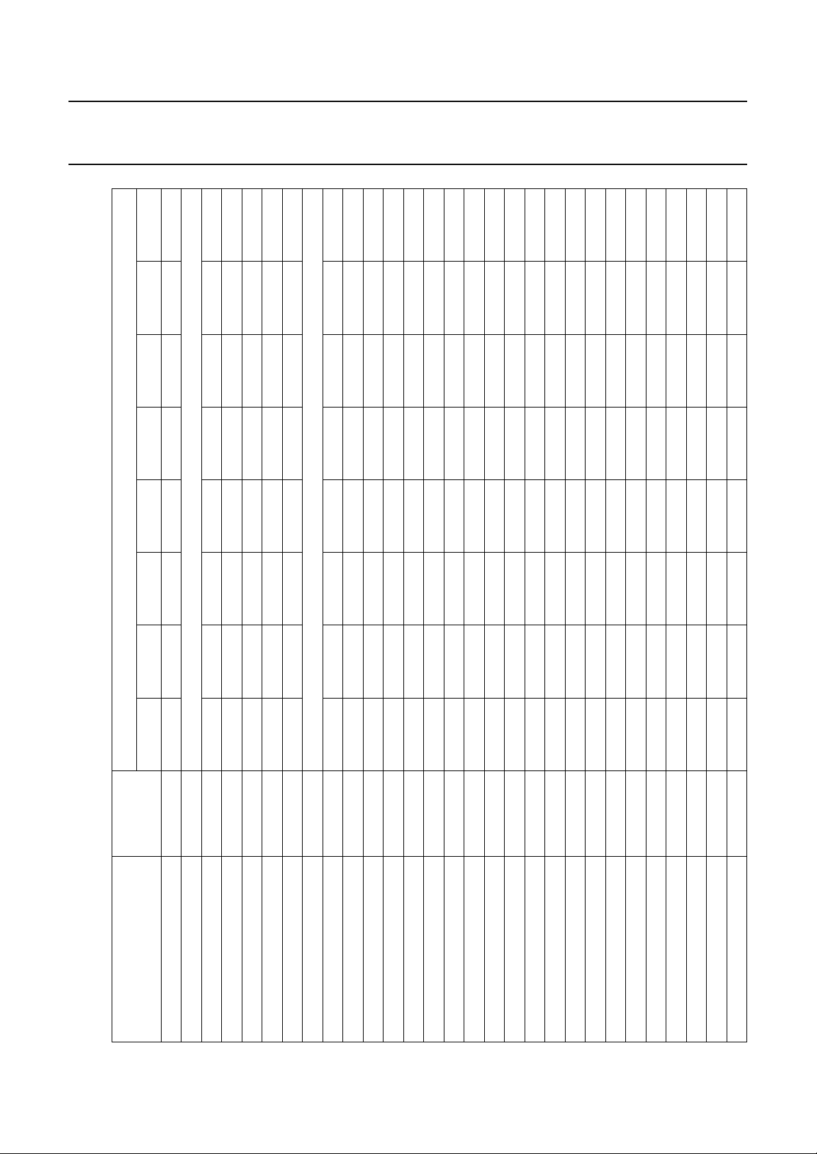
DATA BYTE (note 1)
D7 D6 D5 D4 D3 D2 D1 D0
SUB
ADDRESS
01 to 38 ↓
45 to 56 ↓
REGISTER FUNCTION
Null 00 00000000
Null 39 00000000
Input port control 3A CBENB 0 0 V656 VY2C VUV2C MY2C MUV2C
OSD LUT Y0 42 OSDY07 OSDY06 OSDY05 OSDY04 OSDY03 OSDY02 OSDY01 OSDY00
OSD LUT U0 43 OSDU07 OSDU06 OSDU05 OSDU04 OSDU03 OSDU02 OSDU01 OSDU00
Bit allocation map
Table 4 Slave receiver (slave address 88H or 8CH)
1996 Jul 08 11
OSD LUT V0 44 OSDV07 OSDV06 OSDV05 OSDV04 OSDV03 OSDV02 OSDV01 OSDV00
OSD LUT Y7 57 OSDY77 OSDY76 OSDY75 OSDY74 OSDY73 OSDY72 OSDY71 OSDY70
OSD LUT U7 58 OSDU77 OSDU76 OSDU75 OSDU74 OSDU73 OSDU72 OSDU71 OSDU70
OSD LUT V7 59 OSDV77 OSDV76 OSDV75 OSDV74 OSDV73 OSDV72 OSDV71 OSDV70
Chrominance phase 5A CHPS7 CHPS6 CHPS5 CHPS4 CHPS3 CHPS2 CHPS1 CHPS0
Gain U 5B GAINU7 GAINU6 GAINU5 GAINU4 GAINU3 GAINU2 GAINU1 GAINU0
Gain V 5C GAINV7 GAINV6 GAINV5 GAINV4 GAINV3 GAINV2 GAINV1 GAINV0
Gain U MSB, black level 5D GAINU8 0 BLCKL5 BLCKL4 BLCKL3 BLCKL2 BLCKL1 BLCKL0
Gain V MSB, blanking level 5E GAINV8 0 BLNNL5 BLNNL4 BLNNL3 BLNNL2 BLNNL1 BLNNL0
Null 5F 00000000
Cross-colour select 60 CCRS1 CCRS0 000000
Standard control 61 0 DOWN INPI1 YGS RTCE SCBW PAL FISE
Burst amplitude 62 SQP BSTA6 BSTA5 BSTA4 BSTA3 BSTA2 BSTA1 BSTA0
Subcarrier 0 63 FSC07 FSC06 FSC05 FSC04 FSC03 FSC02 FSC01 FSC00
Subcarrier 1 64 FSC15 FSC14 FSC13 FSC12 FSC11 FSC10 FSC09 FSC08
Subcarrier 2 65 FSC23 FSC22 FSC21 FSC20 FSC19 FSC18 FSC17 FSC16
Subcarrier 3 66 FSC31 FSC30 FSC29 FSC28 FSC27 FSC26 FSC25 FSC24
Line 21 odd 0 67 L21O07 L21O06 L21O05 L21O04 L21O03 L21O02 L21O01 L21O00
Line 21 odd 1 68 L21O17 L21O16 L21O15 L21O14 L21O13 L21O12 L21O11 L21O10
Line 21 even 0 69 L21E07 L21E06 L21E05 L21E04 L21E03 L21E02 L21E01 L21E00
Line 21 even 1 6A L21E17 L21E16 L21E15 L21E14 L21E13 L21E12 L21E11 L21E10
Encoder control, CC line 6B MODIN1 MODIN0 0 SCCLN4 SCCLN3 SCCLN2 SCCLN1 SCCLN0
 Loading...