

Philips saa7182, saa7183 DATASHEETS
INTEGRATED CIRCUITS
DATA SH EET
SAA7182; SAA7183
Digital Video Encoder
(EURO-DENC)
Preliminary specification
Supersedes data of 1995 Sep 19
File under Integrated Circuits, IC22
1996 Jul 08
Philips Semiconductors Preliminary specification
Digital Video Encoder (EURO-DENC) SAA7182; SAA7183
FEATURES
• CMOS 5 V device
• Digital PAL/NTSC/SECAM encoder
• System pixel frequency 13.5 MHz
• Accepts MPEG decoded data on 8-bit wide input port.
Input data format Cb, Y, Cr etc. or Y and Cb, Cr on
16 lines (
“CCIR 656”
)
• Three DACs for CVBS, Y and C operating at 27 MHz
with 10-bit resolution
• Three DACs for RGB operating at 27 MHz with 9-bit
resolution, RGB sync on CVBS and Y
• CVBS, Y, C and RGB output simultaneously
• Closed captioning and teletext encoding including
sequencer and filter
• On-chip YUV to RGB matrix
2
• Fast I
C-bus control port (400 kHz)
• Encoder can be master or slave
• Programmable horizontal and vertical input
synchronization phase
• Programmable horizontal sync output phase
• Internal Colour Bar Generator (CBG)
• Overlay with Look-Up Tables (LUTs) 8 × 3 bytes
• Macrovision Pay-per-View protection system as option,
also used for RGB output
This applies to SAA7183 only. The device is protected
by USA patent numbers 461603, 4577216 and 4819098
and other intellectual property rights.
Use of the Macrovision anti-copy process in the device
is licensed for non-commercial home use only. Reverse
engineering or disassembly is prohibited. Please
contact your nearest Philips Semiconductor sales office
for more information
• Controlled rise/fall times of output syncs and blanking
• Down-mode of DACs
• PLCC84 package.
GENERAL DESCRIPTION
The SAA7182; SAA7183 encodes digital YUV video data
to an NTSC, PAL, SECAM CVBS or S-Video signal and
also RGB.
The circuit accepts CCIR compatible YUV data with
720 active pixels per line in 4:2:2 multiplexed formats,
for example MPEG decoded data. It includes a sync/clock
generator and on-chip Digital-to-Analog Converters
(DACs).
The circuit is compatible to the DIG-TV2 chip family.
QUICK REFERENCE DATA
SYMBOL PARAMETER MIN. TYP. MAX. UNIT
V
V
I
DDA
I
DDD
V
V
DDA
DDD
i
o(p-p)
analog supply voltage 4.75 5.0 5.25 V
digital supply voltage 4.75 5.0 5.25 V
analog supply current − 90 110 mA
digital supply current − 220 250 mA
input signal voltage levels TTL compatible
analog output signal voltages Y, C, CVBS and RGB
− 2 − V
without load (peak-to-peak value)
R
L
load resistance 80 −−Ω
ILE LF integral linearity error −−±2 LSB
DLE LF differential linearity error −−±1 LSB
T
amb
operating ambient temperature 0 − +70 °C
1996 Jul 08 2
Philips Semiconductors Preliminary specification
Digital Video Encoder (EURO-DENC) SAA7182; SAA7183
ORDERING INFORMATION
TYPE NUMBER
PACKAGE
NAME DESCRIPTION VERSION
SAA7182WP PLCC84 plastic leaded chip carrier; 84 leads SOT189-2
SAA7183WP PLCC84 plastic leaded chip carrier; 84 leads SOT189-2
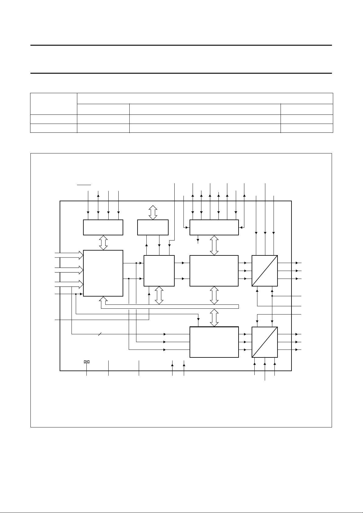
BLOCK DIAGRAM
RTCI
RCV1
TTXRQ
handbook, full pagewidth
10 to 13
16 to 19
DP0
to DP7
MP7
to MP0
OVL2
to OVL0
KEY
TTX
8
25 to 28
31 to 34
8
6 to 8
3
9
21
3, 15, 24,
30, 39, 42,
51, 79, 81
RESET SDA SCL
184834
I2C-BUS
INTERFACE
8
DATA
MANAGER
2
I
C-bus
control
3
V
V
SSD1
SSD9
V
DDD1
V
DDD9
to
to
SA
2
I
C-bus
control
5, 14, 22,
29, 38, 41,
49, 80, 82
CbCr
I2C-bus
control
SECAM
PROCESSOR
DbDr
Y
2, 23, 40, 43,
46, 56, 59,
62, 65, 66
n.c.
8
ENCODER
I2C-bus
8
SAA7182
SAA7183
control
CbCr
SP AP
RCV2
CDIR
50 35 36 20 47 45
37
CLOCK
clock
and timing
Y
OUTPUT
C
control bus
Y
78 77
INTERFACE
internal
PROCESSOR
CREF
SYNC
8
8
8
RGB
XTALO
2
I
control
2
I
control
2
I
control
C-bus
C-bus
C-bus
XTALI
LLC
44 48
V
Y/C/CVBS
V
refH2
53 63
refH1
75
D
D
I
RGB
V
DDA4
to
V
DDA7
68 64, 70,
72, 74
A
A
54,
57, 60
V
DDA1
to
V
DDA3
73
71
69
67
76
52
61
58
55
MGB696
CVBS
Y
CHROMA
V
SSA
V
refL2
V
refL1
RED
GREEN
BLUE
Fig.1 Block diagram.
1996 Jul 08 3
Philips Semiconductors Preliminary specification
Digital Video Encoder (EURO-DENC) SAA7182; SAA7183
PINNING
SYMBOL PIN DESCRIPTION
RESET 1 Reset input, active LOW. After reset is applied, all digital I/Os are in input mode.
The I2C-bus receiver waits for the START condition.
n.c. 2 not connected
V
SSD1
SA 4 The I
V
DDD1
OVL2 6
OVL0 8
KEY 9 Key input for OVL. When HIGH it selects OVL input.
DP0 10
DP1 11
DP2 12
DP3 13
V
DDD2
V
SSD2
DP4 16
DP5 17
DP6 18
DP7 19
TTXRQ 20 Teletext request output, indicating when the bitstream is valid.
TTX 21 Teletext bitstream input.
V
DDD3
n.c. 23 not connected
V
SSD3
MP7 25 Upper 4 bits of MPEG port. It is an input for
MP6 26
MP5 27
MP4 28
V
DDD4
V
SSD4
MP3 31 Lower 4 bits of MPEG port. It is an input for
MP2 32
MP1 33
MP0 34
RCV1 35 Raster Control 1 for video port. This pin receives/provides a VS/FS/FSEQ signal.
RCV2 36 Raster Control 2 for video port. This pin provides an HS pulse of programmable length or
RTCI 37 Real Time Control Input. If the LLC clock is provided by an
3 digital ground 1
2
C-bus slave address select pin. LOW: slave address = 88H, HIGH = 8CH.
5 digital supply voltage 1
3-bit overlay data input. This is the index for the internal look-up table.OVL1 7
Lower 4 bits of the data port. Input for multiplexed Cb, Cr data if 16 line input mode is used.
14 digital supply voltage 2
15 digital ground 2
Upper 4 bits of the data port. Input for multiplexed Cb, Cr data if 16 line input mode is used.
22 digital supply voltage 3
24 digital ground 3
input for Y data only, if 16 line input mode is used.
29 digital supply voltage 4
30 digital ground 4
input for Y data only, if 16 line input mode is used.
receives an HS pulse.
should be connected to the RTCO pin of the respective decoder to improve the signal quality.
“CCIR 656”
“CCIR 656”
style multiplexed Cb, Y, Cr data, or
style multiplexed Cb, Y, Cr data, or
SAA7111
or
SAA7151B
, RTCI
1996 Jul 08 4
Philips Semiconductors Preliminary specification
Digital Video Encoder (EURO-DENC) SAA7182; SAA7183
SYMBOL PIN DESCRIPTION
V
DDD5
V
SSD5
n.c. 40 not connected
V
DDD6
V
SSD6
n.c. 43 not connected
XT ALI 44 Crystal oscillator input (from crystal). If the oscillator is not used, this pin should be connected
XTALO 45 Crystal oscillator output (to crystal).
n.c. 46 not connected
CREF 47 Clock Reference signal. This is the clock qualifier for DIG-TV2 compatible signals.
LLC 48 Line-Locked Clock. This is the 27 MHz master clock for the encoder. The I/O direction is set
V
DDD7
CDIR 50 Clock direction. If the CDIR input is HIGH, the circuit receives a clock and optional CREF
V
SSD7
V
refL1
V
refH1
V
DDA1
BLUE 55 Analog output of the BLUE component.
n.c. 56 not connected
V
DDA2
GREEN 58 Analog output of the GREEN component.
n.c. 59 not connected
V
DDA3
RED 61 Analog output of the RED component.
n.c. 62 not connected
I
RGB
V
DDA4
n.c. 65 not connected
n.c. 66 not connected
V
SSA
I
Y/C/CVBS
CHROMA 69 Analog output of the chrominance signal.
V
DDA5
Y 71 Analog output of the luminance signal.
V
DDA6
CVBS 73 Analog output of the CVBS signal.
38 digital supply voltage 5
39 digital ground 5
41 digital supply voltage 6
42 digital ground 6
to ground.
by the CDIR pin.
49 digital supply voltage 7
signal, otherwise if CDIR is LOW CREF and LLC are generated by the internal crystal
oscillator.
51 digital ground 7
52 Lower reference voltage 1 input for the RGB DACs, connect to V
SSA
.
53 Upper reference voltage 1 input for the RGB DACs, connect via 100 nF capacitor to V
54 Analog supply voltage 1 for the RGB DACs.
57 Analog supply voltage 2 for the RGB DACs.
60 Analog supply voltage 3 for the RGB DACs.
63 Current input for RGB amplifiers, connected via 15 kΩ resistor to V
DDA
.
64 Analog supply voltage 4 for the Y/C/CVBS DACs.
67 Analog ground for the DACs.
68 Current input for the Y/C/CVBS amplifiers, connected via 15 kΩ resistor to V
DDA
.
70 Analog supply voltage 5 for the Y/C/CVBS DACs.
72 Analog supply voltage 6 for the Y/C/CVBS DACs.
SSA.
1996 Jul 08 5
Philips Semiconductors Preliminary specification
Digital Video Encoder (EURO-DENC) SAA7182; SAA7183
SYMBOL PIN DESCRIPTION
V
DDA7
V
refH2
V
refL2
AP 77 Test pin. Connected to digital ground for normal operation.
SP 78 Test pin. Connected to digital ground for normal operation.
V
SSD8
V
DDD8
V
SSD9
V
DDD9
SCL 83 I
SDA 84 I
74 Analog supply voltage 6 for the Y/C/CVBS DACs.
75 Upper reference voltage 2 input for the Y/C/CVBS DACs, connected via 100 nF capacitor to
V
SSA.
76 Lower reference voltage 2 input for the Y/C/CVBS DACs, connect to V
SSA
.
79 digital ground 8
80 digital supply voltage 8
81 digital ground 9
82 digital supply voltage 9
2
C-bus serial clock input.
2
C-bus serial data input/output.
1996 Jul 08 6
Philips Semiconductors Preliminary specification
Digital Video Encoder (EURO-DENC) SAA7182; SAA7183
handbook, full pagewidth
DP1
11
DP0
10
KEY
9
OVL0
8
OVL1
7
OVL2
6
DDD1
V
5
SA
4
SSD1
V
3
n.c.
2
RESET
1
SDA
84
DDD9VSSD9VDDD8VSSD8
SCL
V
83
82
81
AP
77
refL2VrefH2
V
76
75
SP
80
79
78
DP3
V
DDD2
V
SSD2
DP4
DP5
DP6
DP7
TTXRQ
TTX
V
DDD3
n.c.
V
SSD3
MP7
MP6
MP5
MP4
V
DDD4
V
SSD4
MP3
MP2
12DP2
13
14
15
16
17
18
19
20
21
74
73
72
71
70
69
68
67
66
65
V
DDA7
CVBS
V
DDA6
Y
V
DDA5
CHROMA
I
Y/C/CVBS
V
SSA
n.c.
n.c.
SAA7182
22
23
24
25
26
27
28
29
30
31
32
SAA7183
64
63
62
61
60
59
58
57
56
55
54
V
DDA4
I
RGB
n.c.
RED
V
DDA3
n.c.
GREEN
V
DDA2
n.c.
BLUE
V
DDA1
33
34
35
36
37
38
39
40
41
42
MP1
MP0
RCV1
RCV2
RTCI
DDD5
V
SSD5
V
n.c.
DDD6
V
SSD6
V
Fig.2 Pin configuration.
1996 Jul 08 7
43
n.c.
44
XTALI
45
XTALO
46
n.c.
47
CREF
48
LLC
49
DDD7
V
50
CDIR
51
SSD7
V
52
refL1
V
53
refH1
V
MGB697

Philips Semiconductors Preliminary specification
Digital Video Encoder (EURO-DENC) SAA7182; SAA7183
FUNCTIONAL DESCRIPTION
The digital video encoder (EURO-DENC) encodes digital
luminance and colour difference signals into analog CVBS
and simultaneously S-Video signals. NTSC-M, PAL B/G
and SECAM standards and sub-standards are supported.
Both interlaced and non-interlaced operation is possible
for all standards.
In addition to RED, GREEN and BLUE converted
components, the dematrixed YUV input is available on
three separate analog outputs.
The basic encoder function consists of subcarrier
generation and colour modulation also insertion of
synchronization signals. Luminance and chrominance
signals are filtered in accordance with the standard
requirements of RS-170-A and
For ease of analog post filtering the signals are twice
oversampled with respect to the pixel clock before
digital-to-analog conversion.
For total filter transfer characteristics see
Figs 3, 4, 5, 6, 7 and 8. The DACs for Y, C and CVBS are
realized with full 10-bit resolution, DACs for RGB are with
9-bit resolution.
The MPEG port (MP) accept 8 lines multiplexed Cb-Y-Cr
data.
The 8-bit multiplexed Cb-Y-Cr formats are
(D1 format) compatible, but the SAV, EAV etc. codes are
not decoded.
Alternatively, 8-bits Y on MP port and 8-bit multiplexed Cb,
Cr on DP port can be chosen as input.
A crystal-stable master clock (LLC) of 27 MHz, which is
twice the CCIR line-locked pixel clock of 13.5 MHz, needs
to be supplied externally. Optionally, a crystal oscillator
input/output pair of pins and an on-chip clock driver is
provided.
It is also possible to connect a Philips Digital Video
Decoder (SAA7111 or SAA7151B) in conjunction with a
CREF clock qualifier to EURO-DENC. Via RTCI pin
connected to RTCO of a decoder, information concerning
actual subcarrier, PAL-ID (see
definite subcarrier phase can be inserted.
“CCIR 624”
“data sheet SAA7111”
.
“CCIR 656”
)
European teletext encoding is supported if an appropriate
teletext bitstream is applied to the TTX pin.
The IC also contains Closed Caption and Extended Data
Services Encoding (Line 21), and supports anti-taping
signal generation in accordance with Macrovision; it also
supports overlay via KEY and three control bits by a 24 × 8
LUT.
A number of possibilities are provided for setting of
different video parameters such as:
Black and blanking level control
Colour subcarrier frequency
Variable burst amplitude etc.
During reset (
all digital I/O stages are set to input mode. A reset forces
the I2C-bus interface to abort any running bus transfer and
sets register 3A to 03H, register 61 to 06H and
registers 6BH and 6EH to 00H. All other control registers
are not influenced by a reset.
Data manager
In the data manager, real time arbitration on the data
stream to be encoded is performed.
Depending on the polarity of pin KEY, the MP input
(or MP/DP input) or OVL input are selected to be encoded
to CVBS and Y/C signals, and output as RGB.
KEY controls OVL entries of a programmable LUT for
encoded signals and for RGB output. The common KEY
switching signal can be disabled by software for the
signals to be encoded (Y, C and CVBS), such that OVL will
appear on RGB outputs, but not on Y, C and CVBS.
OVL input under control of KEY can be also used to insert
decoded teletext information or other on-screen data.
Optionally, the OVL colour LUTs located in this block, can
be read out in a pre-defined sequence (8 steps per active
video line), achieving, for example, a colour bar test
pattern generator without need for an external data
source. The colour bar function is only under software
control.
RESET = LOW) and after reset is released,
The EURO-DENC synthesizes all necessary internal
signals, colour subcarrier frequency, and synchronization
signals, from that clock. The encoder is always timing
master for the MPEG port (MP), but it can additionally be
configured as slave with respect to the RCV trigger inputs.
1996 Jul 08 8

Philips Semiconductors Preliminary specification
Digital Video Encoder (EURO-DENC) SAA7182; SAA7183
Encoder
V
IDEO PATH
The encoder generates out of Y, U and V baseband
signals luminance and colour subcarrier output signals,
suitable for use as CVBS or separate Y and C signals.
Luminance is modified in gain and in offset (latter
programmable in a certain range to enable different black
level set-ups). After having been inserted a fixed
synchronization level, in accordance with standard
composite synchronization schemes, and blanking level,
programmable also in a certain range to allow for
manipulations with Macrovision anti-taping, additional
insertion of AGC super-white pulses, programmable in
height, is supported.
In order to enable easy analog post filtering, luminance is
interpolated from 13.5 MHz data rate to 27 MHz data rate,
providing luminance in 10-bit resolution. This filter is also
used to define smoothed transients for synchronization
pulses and blanking period. For transfer characteristic of
the luminance interpolation filter see Figs 5 and 6.
Chrominance is modified in gain (programmable
separately for U and V), standard dependent burst is
inserted, before baseband colour signals are interpolated
from 6.75 MHz data rate to 27 MHz data rate. One of the
interpolation stages can be bypassed, thus providing a
higher colour bandwidth, which can be made use of for Y/C
output. For transfer characteristics of the chrominance
interpolation filter see Figs 3 and 4.
The amplitude of inserted burst is programmable in a
certain range, suitable for standard signals and for special
effects. Behind the succeeding quadrature modulator,
colour in 10-bit resolution is provided on subcarrier.
The numeric ratio between Y and C outputs is in
accordance with set standards.
C
LOSED CAPTION ENCODER
Using this circuit, data in accordance with the specification
of Closed Caption or Extended Data Service, delivered by
the control interface, can be encoded (Line 21). Two
dedicated pairs of bytes (two bytes per field), each pair
preceded by run-in clocks and framing code, are possible.
The actual line number where data is to be encoded in, can
be modified in a certain range.
Data clock frequency is in accordance with definition for
NTSC-M standard 32 times horizontal line frequency.
Data LOW at the output of the DACs corresponds to 0 IRE,
data HIGH at the output of the DACs corresponds to
approximately 50 IRE.
It is also possible to encode Closed Caption Data for 50 Hz
field frequencies at 32 times horizontal line frequency.
NTI-TAPING (SAA7183 ONLY)
A
For more information contact your nearest Philips
Semiconductors sales office.
RGB processor
This block contains a dematrix in order to produce RED,
GREEN and BLUE signals to be fed to a SCART plug.
Before Y, Cb, Cr signals are dematrixed, 2 times
oversampling for luminance and 4 times oversampling for
colour difference signals is performed. For transfer curves
of luminance and colour difference components of RGB
see Figs 7 and 8.
SECAM processor
SECAM specific pre-processing is achieved in this block
by a pre-emphasis of colour difference signals (for gain
and phase see Figs 9 and 10.
ELETEXT INSERTION AND ENCODING
T
Pin TTX receives a teletext bitstream sampled at the LLC
clock, each teletext bit is carried by four or three LLC
samples.
Phase variant interpolation is achieved on this bitstream in
the internal teletext encoder, providing sufficient small
phase jitter on the output text lines.
TTXRQ provides a fully programmable request signal to
the teletext source, indicating the insertion period of
bitstream at lines selectable independently for both fields.
The internal insertion window for text is set to 360 teletext
bits including clock run-in bits. For protocol and timing see
Fig.17.
1996 Jul 08 9
A baseband frequency modulator with a reference
frequency shifted from 4.286 MHz to DC carries out
SECAM modulation in accordance with appropriate
standard or optionally wide clipping limits.
After the HF pre-emphasis, also applied on a DC reference
carrier (anti-Cloche filter; see Figs 11 and 12), line-by-line
sequential carriers with black reference of 4.25 MHz (Db)
and 4.40625 MHz (Dr) are generated using specified
values for FSC programming bytes.
Alternating phase reset in accordance with SECAM
standard is carried out automatically. During vertical
blanking the so-called bottle pulses are not provided.

Philips Semiconductors Preliminary specification
Digital Video Encoder (EURO-DENC) SAA7182; SAA7183
Output interface/DACs
In the output interface encoded both Y and C signals are
converted from digital-to-analog in 10-bit resolution. Y and
C signals are also combined to a 10-bit CVBS signal.
The CVBS output occurs with the same processing delay
as the Y and C outputs. Absolute amplitudes at the input
of the DAC for CVBS is reduced by15⁄16 with respect to Y
and C DACs to make maximum use of conversion ranges.
RED, GREEN and BLUE signals are also converted from
digital-to-analog, each providing a 9-bit resolution.
Outputs of the DACs can be set together in two groups via
software control to minimum output voltage for either
purpose.
Synchronization
Synchronization of the EURO-DENC is able to operate in
two modes; slave mode and master mode.
In the slave mode, the circuit accepts synchronization
pulses at the bidirectional RCV1 port. The timing and
trigger behaviour related to RCV1 can be influenced by
programming the polarity and on-chip delay of RCV1.
Active slope of RCV1 defines the vertical phase and
optionally the odd/even and colour frame phase to be
initialized, it can be also used to set the horizontal phase.
If the horizontal phase is not be influenced by RCV1, a
horizontal pulse needs to be supplied at the RCV2 pin.
Timing and trigger behaviour can also be influenced for
RCV2.
If there are missing pulses at RCV1 and/or RCV2, the time
base of EURO-DENC runs free, thus an arbitrary number
of synchronization slopes may miss, but no additional
pulses (such with wrong phase) must occur.
If the vertical and horizontal phase is derived from RCV1,
RCV2 can be used for horizontal or composite blanking
input or output.
On the RCV2 port, the IC can provide a horizontal pulse
with programmable start and stop phase; this pulse can be
inhibited in the vertical blanking period to build up, for
example, a composite blanking signal.
The polarity of both RCV1 and RCV2 is selectable by
software control.
Field length is in accordance with 50 Hz or 60 Hz
standards, including non-interlaced options; start and end
of its active part can be programmed. The active part of a
field always starts at the beginning of a line, if the standard
blanking option SBLBN is not set.
2
C-bus interface
I
The I2C-bus interface is a standard slave transceiver,
supporting 7-bit slave addresses and 400 kbits/s
guaranteed transfer rate. It uses 8-bit subaddressing with
an auto-increment function. All registers are write only,
except one readable status byte.
Two I2C-bus slave addresses are selected:
88H: LOW at pin 4
8CH: HIGH at pin 4.
Input levels and formats
EURO-DENC expects digital Y, Cb, Cr data with levels
(digital codes) in accordance with
For C and CVBS outputs, deviating amplitudes of the
colour difference signals can be compensated by
independent gain control setting, while gain for luminance
is set to predefined values, distinguishable for 7.5 IRE
set-up or without set-up.
For RGB outputs fixed amplification in accordance with
“CCIR 601”
Reference levels are measured with a colour bar,
100% white, 100% amplitude and 100% saturation.
is provided.
“CCIR 601”
.
In the master mode, the time base of the circuit
continuously runs free. On the RCV1 port, the IC can
output:
• A Vertical Sync signal (VS) with 3 or 2.5 lines duration,
or
• An ODD/EVEN signal which is LOW in odd fields, or
• A field sequence signal (FSEQ) which is HIGH in the first
of 4 respectively 8 respectively 12 fields.
1996 Jul 08 10
Philips Semiconductors Preliminary specification
Digital Video Encoder (EURO-DENC) SAA7182; SAA7183
Table 1
“CCIR 601”
COLOUR
signal component levels
SIGNALS
YCbCrR
(1)
(2)
(2)
G
B
White 235 128 128 235 235 235
Yellow 210 16 146 235 235 16
Cyan 170 166 16 16 235 235
Green 145 54 34 16 235 16
Magenta 106 202 222 235 16 235
Red 81 90 240 235 16 16
Blue 41 240 110 16 16 235
Black 16 128 128 16 16 16
Notes
1. Transformation:
a) R = Y + 1.3707 × (Cr − 128)
b) G = Y − 0.3365 × (Cb − 128) − 0.6982 × (Cb − 128)
c) B = Y + 1.7324 × (Cb − 128).
2. Representation of R, G and B at the output is 9 bits at 27 MHz.
Table 2 8-bit multiplexed format (similar to
“CCIR 601”
)
(2)
TIME 0 1 2 2 4 5 6 7
Sample Cb
0
Y
0
Cr
0
Y
1
Cb
2
Y
2
Cr
2
Luminance pixel number 0 1 2 3
Colour pixel number 0 2
Table 3 16-bit multiplexed format (DTV2 format)
TIME 0 1 2 3 4 5 6 7
Sample Y line Y
Sample UV line Cb
0
0
Y
Cr
1
0
Y
Cb
2
2
Luminance pixel number 0 1 2 3
Colour pixel number 0 2
Cr
Y
3
Y
3
2
1996 Jul 08 11

Philips Semiconductors Preliminary specification
Digital Video Encoder (EURO-DENC) SAA7182; SAA7183
DATA BYTE
D7 D6 D5 D4 D3 D2 D1 D0
SUB
ADDRESS
↓↓
↓↓
5E GAINV8 DECTYP BLNNL5 BLNNL4 BLNNL3 BLNNL2 BLNNL1 BLNNL0
REGISTER FUNCTION
Null 00 00000000
Null 39 00000000
Input port control 3A CBENB DISKEY 0 0 0 FMT16 Y2C UV2C
OVL LUT Y0 42 OVLY07 OVLY06 OVLY05 OVLY04 OVLY03 OVLY02 OVLY01 OVLY00
OVL LUT U0 43 OVLU07 OVLU06 OVLU05 OVLU04 OVLU03 OVLU02 OVLU01 OVLU00
Bit allocation map
Table 4 Slave Receiver (Slave Address 88H or 8CH)
1996 Jul 08 12
OVL LUT V0 44 OVLV07 OVLV06 OVLV05 OVLV04 OVLV03 OVLV02 OVLV01 OVLV00
OVL LUT Y7 57 OVLY77 OVLY76 OVLY75 OVLY74 OVLY73 OVLY72 OVLY71 OVLY70
OVL LUT U7 58 OVLU77 OVLU76 OVLU75 OVLU74 OVLU73 OVLU72 OVLU71 OVLU70
OVL LUT V7 59 OVLV77 OVLV76 OVLV75 OVLV74 OVLV73 OVLV72 OVLV71 OVLV70
Chrominance phase 5A CHPS7 CHPS6 CHPS5 CHPS4 CHPS3 CHPS2 CHPS1 CHPS0
Gain U 5B GAINU7 GAINU6 GAINU5 GAINU4 GAINU3 GAINU2 GAINU1 GAINU0
Gain V 5C GAINV7 GAINV6 GAINV5 GAINV4 GAINV3 GAINV2 GAINV1 GAINV0
Gain U MSB, black level 5D GAINU8 0 BLCKL5 BLCKL4 BLCKL3 BLCKL2 BLCKL1 BLCKL0
Gain V MSB, blanking level,
decoder type
Blanking level VBI 5F 0 0 BLNVB5 BLNVB4 BLNVB3 BLNVB2 BLNVB1 BLNVB0
Null 60 00000000
Standard control 61 DOWNB DOWNA INPI YGS SECAM SCBW PAL FISE
Burst amplitude 62 RTCE BSTA6 BSTA5 BSTA4 BSTA3 BSTA2 BSTA1 BSTA0
Subcarrier 0 63 FSC07 FSC06 FSC05 FSC04 FSC03 FSC02 FSC01 FSC00
Subcarrier 1 64 FSC15 FSC14 FSC13 FSC12 FSC11 FSC10 FSC09 FSC08
Subcarrier 2 65 FSC23 FSC22 FSC21 FSC20 FSC19 FSC18 FSC17 FSC16
Subcarrier 3 66 FSC31 FSC30 FSC29 FSC28 FSC27 FSC26 FSC25 FSC24
Line 21 odd 0 67 L21O07 L21O06 L21O05 L21O04 L21O03 L21O02 L21O01 L21O00
Line 21 odd 1 68 L21O17 L21O16 L21O15 L21O14 L21O13 L21O12 L21O11 L21O10
Line 21 even 0 69 L21E07 L21E06 L21E05 L21E04 L21E03 L21E02 L21E01 L21E00
Line 21 even 1 6A L21E17 L21E16 L21E15 L21E14 L21E13 L21E12 L21E11 L21E10
 Loading...