

Philips SAA716WP5 Datasheet

DATA SH EET
Product specification
Supersedes data of May 1995
File under Integrated Circuits, IC22
1996 Aug 20
INTEGRATED CIRCUITS
SAA7165
Video Enhancement and
Digital-to-Analog processor
(VEDA2)
1996 Aug 20 2
Philips Semiconductors Product specification
Video Enhancement and
Digital-to-Analog processor (VEDA2)
SAA7165
FEATURES
• CMOS circuit to enhance video data and to convert
luminance and colour-difference signals from
digital-to-analog
• Digital Colour Transient Improvement block (DCTI) to
increase the sharpness of colour transitions.
The improved pin-compatible SAA7165 can supersede
the SAA9065
• 16-bit parallel input for 4 : 1 : 1 and 4:2:2 YUV data
• Data clock input LLC (Line-Locked Clock) for a data rate
up to 36 MHz
• 8-bit luminance and 8-bit multiplexed colour-difference
formats (7-bit formats optional)
• MC input to support various clock and pixel rates
• Formatting YUV input data; 4 :2:2format,
4:1:1format and filter characteristics selectable
• HREF input to determine the active line (number of
pixels)
• Controllable peaking of luminance signal
• Coring stage with controllable threshold to eliminate
noise in luminance signal
• Interpolation filter suitable for both formats to increase
the data rate in chrominance path
• Polarity of colour-difference signals selectable
• All functions controlled via I
2
C-bus
• Separate digital-to-analog converters (9-bit resolution
for Y; 8-bit for colour-difference signals)
• 1 V (p-p)/75 Ω outputs realized by two resistors
• No external adjustments.
QUICK REFERENCE DATA
ORDERING INFORMATION
SYMBOL PARAMETER MIN. TYP. MAX. UNIT
V
DDD
digital supply voltage 4.5 5 5.5 V
V
DDA
analog supply voltage 4.75 5 5.25 V
I
DD(tot)
total supply current − tbf − mA
V
IL
LOW-level input voltage on YUV-bus −0.5 − +0.8 V
V
IH
HIGH-level input voltage on YUV-bus 2 − V
DDD
+ 0.5 V
f
LLC
input data rate −−36 MHz
V
o(p-p)
output signals Y, (R − Y) and (B − Y) (peak-to-peak value) − 2 − V
R
L
output load resistance 125 −− Ω
ILE DC integral linearity error in output signal (8-bit data) −−1 LSB
DLE DC differential error in output signal (8-bit data) −−0.5 LSB
T
amb
operating ambient temperature range 0 − 70 °C
TYPE
NUMBER
PACKAGE
NAME DESCRIPTION VERSION
SAA7165WP PLCC44 plastic leaded chip carrier; 44 leads SOT187-2
1996 Aug 20 3
Philips Semiconductors Product specification
Video Enhancement and Digital-to-Analog
processor (VEDA2)
SAA7165
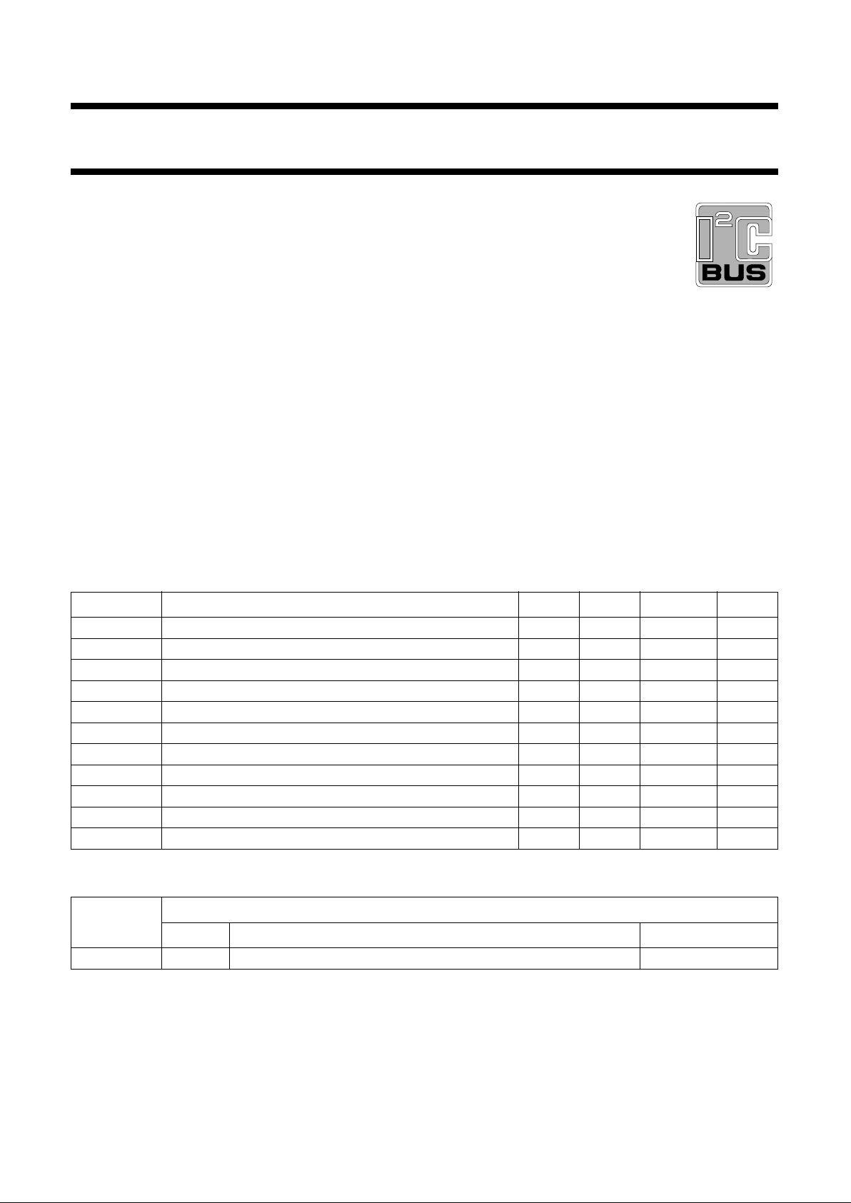
BLOCK DIAGRAM
handbook, full pagewidth
MEH464
INTERPOLATION
FILTER
Y
FORMATTER
DCTI
SAA7165
Y
U
V
DATA
SWITCH
DAC 3
41 42
CUR
V
DDA4
25 Ω
36
PEAKING
AND
CORING
DAC 2
DAC 1
UV
FORMATTER
TIMING
CONTROL
I
2
C-BUS
CONTROL
TEST
CONTROL
40
V
DDA3
37
V
DDA2
32
V
DDA1
31
V
DDD2
12
13
V
SSD1
V
DDD1
data clock
21 to 14
8
Y7 to Y0
11 to 4
242725
26
28
29
8
UV7 to
UV0
MC
LLC
HREF
RESET
SCL
SDA
YUV-bus
I
2
C-bus
25 Ω
33
(R − Y)
(B − Y)
25 Ω
39
1
Y
C
UV
REFL
UV
REFL
Y
2
C
Y
43
44
30
V
SSD2
22
AP
23
SP
34
V
SSA1
35
V
SSA2
38
V
SSA3
3
SUB
Fig.1 Block diagram.

1996 Aug 20 4
Philips Semiconductors Product specification
Video Enhancement and Digital-to-Analog
processor (VEDA2)
SAA7165
PINNING
SYMBOL PIN DESCRIPTION
REFL
Y
1 low reference of luminance DAC (connected to V
SSA1
)
C
Y
2 capacitor for luminance DAC (high reference)
SUB 3 substrate (connected to V
SSA1
)
UV0 4 UV signal input bit UV7 (digital colour-difference signal)
UV1 5 UV signal input bit UV6 (digital colour-difference signal)
UV2 6 UV signal input bit UV5 (digital colour-difference signal)
UV3 7 UV signal input bit UV4 (digital colour-difference signal)
UV4 8 UV signal input bit UV3 (digital colour-difference signal)
UV5 9 UV signal input bit UV2 (digital colour-difference signal)
UV6 10 UV signal input bit UV1 (digital colour-difference signal)
UV7 11 UV signal input bit UV0 (digital colour-difference signal)
V
DDD1
12 +5 V digital supply voltage 1
V
SSD1
13 digital ground 1 (0 V)
Y0 14 Y signal input bit Y7 (digital luminance signal)
Y1 15 Y signal input bit Y6 (digital luminance signal)
Y2 16 Y signal input bit Y5 (digital luminance signal)
Y3 17 Y signal input bit Y4 (digital luminance signal)
Y4 18 Y signal input bit Y3 (digital luminance signal)
Y5 19 Y signal input bit Y2 (digital luminance signal)
Y6 20 Y signal input bit Y1 (digital luminance signal)
Y7 21 Y signal input bit Y0 (digital luminance signal)
AP 22 connected to ground (action pin for testing)
SP 23 connected to ground (shift pin for testing)
MC 24 data clock CREF (e.g. 13.5 MHz); at MC = HIGH, the LLC divider-by-two is inactive
LLC 25 line-locked clock signal (LL27 = 27 MHz)
HREF 26 data clock for YUV data inputs (for active line 768Y or 640Y long)
RESET 27 reset input (active LOW)
SCL 28 I
2
C-bus clock line
SDA 29 I
2
C-bus data line
V
SSD2
30 digital ground 2 (0 V)
V
DDD2
31 +5 V digital supply voltage 2
V
DDA1
32 +5 V analog supply voltage for buffer of DAC 1
(R − Y) 33 ±(R − Y) output signal (analog signal)
V
SSA1
34 analog ground 1 (0 V)
V
SSA2
35 analog ground 2 (0 V)
(B − Y) 36 ±(B − Y) output signal (analog colour-difference signal)
V
DDA2
37 +5 V analog supply voltage for buffer of DAC 2
V
SSA3
38 analog ground 3 (0 V)
Y 39 Y output signal (analog luminance signal)
V
DDA3
40 +5 V analog supply voltage for buffer of DAC 3
1996 Aug 20 5
Philips Semiconductors Product specification
Video Enhancement and Digital-to-Analog
processor (VEDA2)
SAA7165
CUR 41 current input for analog output buffers
V
DDA4
42 supply and reference voltage for the three DACs
C
UV
43 capacitor for chrominance DACs (high reference)
REFL
UV
44 low reference of chrominance DACs (connected to V
SSA1
)
SYMBOL PIN DESCRIPTION
Fig.2 Pin configuration.
handbook, full pagewidth
SAA7165
MEH465
7
8
9
10
11
12
13
14
15
16
17
39
38
37
36
35
34
33
32
31
30
29
18
19
20
21
22
23
24
25
26
27
28
6
5
4
3
2
1
44
43
42
41
40
Y
SDA
V
SSA3
V
SSD2
V
SSA2
V
SSA1
V
DDA2
V
DDA1
V
DDD2
(B − Y)
(R − Y)
UV1
UV0
SUB
CYREFLYREFLUVC
UV
CUR
V
DDA4
V
DDA3
UV2
UV3
UV4
UV5
UV6
UV7
Y0
Y1
Y2
Y3
Y4
Y5
Y6
Y7
AP
SP
MC
LLC
HREF
RESET
SCL
V
DDD1
V
SSD1
1996 Aug 20 6
Philips Semiconductors Product specification
Video Enhancement and Digital-to-Analog
processor (VEDA2)
SAA7165
FUNCTIONAL DESCRIPTION
The CMOS circuit SAA7165 processes digital YUV-bus
data up to a data rate of 36 MHz. The data inputs Y7 to Y0
and UV7 to UV0 (see Fig.1) are provided with 8-bit data.
The data of digital colour-difference signals U and V are in
a multiplexed state (serial in 4 : 2:2or4:1:1format;
Tables 2 and 3).
Data is read with the rising edge of LLC (Line-Locked
Clock) to achieve a data rate of LLC at MC = HIGH only. If
MC is supplied with the frequency CREF (1⁄2LLC for
example), data is read only at every second rising edge
(see Fig.3).
The 7-bit YUV input data are also supported by means of
bit R78 (R78 = 0). Additionally, the luminance data format
is converted for internal use into a two´s complement
format by inverting the MSB. The Y input byte
(bits Y7 to Y0) represents luminance information; the UV
input byte (bits UV7 to UV0) represents one of the two
digital colour-difference signals in 4 :2:2format
(Table 2).
The HREF input signal (HREF = HIGH) determines the
start and the end of an active line (see Fig.3) and the
number of pixels respectively. The analog output Y is
blanked at HREF = LOW, the (B − Y) and (R − Y) outputs
are in a colourless state. The blanking level can be set with
bit BLV. The SAA7165 is controllable via the I
2
C-bus.
Formatting Y and UV
The input data formats are formatted into the internally
used processing formats (separate for 4 :2:2 and
4:1:1formats). The IFF, IFC and IFL bits control the
input data format and determine the right interpolation filter
(see Figs 10 to 13).
Peaking and coring
Peaking is applied to the Y signal to compensate several
bandwidth reductions of the external pre-processing.
Y signals can be improved to obtain a better sharpness.
There are the two switchable bandpass filters
BF1 and BF2 controlled via the I
2
C-bus by the bits BP1,
BP0 and BFB. Thus, a frequency response is achieved in
combination with the peaking factor K (Figs 5 to 9;
K is determined by the bits BFB, WG1 and WG0).
The coring stage with controllable threshold (4 states
controlled by CO1 and CO0 bits) reduces noise
disturbances (generated by the bandpass gain) by
suppressing the amplitude of small high-frequent signal
components. The remaining high-frequent peaking
component is available for a weighted addition after
coring.
Table 1 LLC and MC configuration modes in DMSD applications (note 1)
Note
1. YUV data are only latched with the rising edge of LCC at MC = HIGH.
PIN INPUT SIGNAL DESCRIPTION
LLC LLC (LL27) The data rate on YUV-bus is half the clock rate on pin LLC, e.g. in
SAA7151B, SAA7191 and SAA7191B single scan operation.
MC CREF
LLC LLC (LL27) The data rate on YUV-bus must be identical to the clock rate on pin LLC,
e.g. in double scan applications.
MC MC = HIGH
LLC LLC (LL27) The data rate on YUV-bus must be identical to the clock rate on pin LLC,
e.g. SAA9051 single scan operation.
MC MC = HIGH
1996 Aug 20 7
Philips Semiconductors Product specification
Video Enhancement and Digital-to-Analog
processor (VEDA2)
SAA7165
Table 2 Data format 4 :2:2
Table 3 Data format 4 :1:1
INPUT PIXEL BYTE SEQUENCE (4:2:2FORMAT)
Y0 (LSB) Y0 Y0 Y0 Y0 Y0 Y0
Y1 Y1 Y1 Y1 Y1 Y1 Y1
Y2 Y2 Y2 Y2 Y2 Y2 Y2
Y3 Y3 Y3 Y3 Y3 Y3 Y3
Y4 Y4 Y4 Y4 Y4 Y4 Y4
Y5 Y5 Y5 Y5 Y5 Y5 Y5
Y6 Y6 Y6 Y6 Y6 Y6 Y6
Y7 (MSB) Y7 Y7 Y7 Y7 Y7 Y7
UV0 (LSB) U0 V0 U0 V0 U0 V0
UV1 U1 V1 U1 V1 U1 V1
UV2 U2 V2 U2 V2 U2 V2
UV3 U3 V3 U3 V3 U3 V3
UV4 U4 V4 U4 V4 U4 V4
UV5 U5 V5 U5 V5 U5 V5
UV6 U6 V6 U6 V6 U6 V6
UV7 (MSB) U7 V7 U7 V7 U7 V7
Y frame 012345
UV frame 0 2 4
INPUT PIXEL BYTE SEQUENCE (4:1:1FORMAT)
Y0 Y0 Y0 Y0 Y0 Y0 Y0 Y0 Y0
Y1 Y1 Y1 Y1 Y1 Y1 Y1 Y1 Y1
Y2 Y2 Y2 Y2 Y2 Y2 Y2 Y2 Y2
Y3 Y3 Y3 Y3 Y3 Y3 Y3 Y3 Y3
Y4 Y4 Y4 Y4 Y4 Y4 Y4 Y4 Y4
Y5 Y5 Y5 Y5 Y5 Y5 Y5 Y5 Y5
Y6 Y6 Y6 Y6 Y6 Y6 Y6 Y6 Y6
Y7 Y7 Y7 Y7 Y7 Y7 Y7 Y7 Y7
UV0 00000000
UV1 00000000
UV2 00000000
UV3 00000000
UV4 V6 V4 V2 V0 V6 V4 V2 V0
UV5 V7 V5 V3 V1 V7 V5 V3 V1
UV6 U6 U4 U2 U0 U6 U4 U2 U0
UV7 U7 U5 U3 U1 U7 U5 U3 U1
Y frame 01234567
UV frame 0 4
1996 Aug 20 8
Philips Semiconductors Product specification
Video Enhancement and Digital-to-Analog
processor (VEDA2)
SAA7165
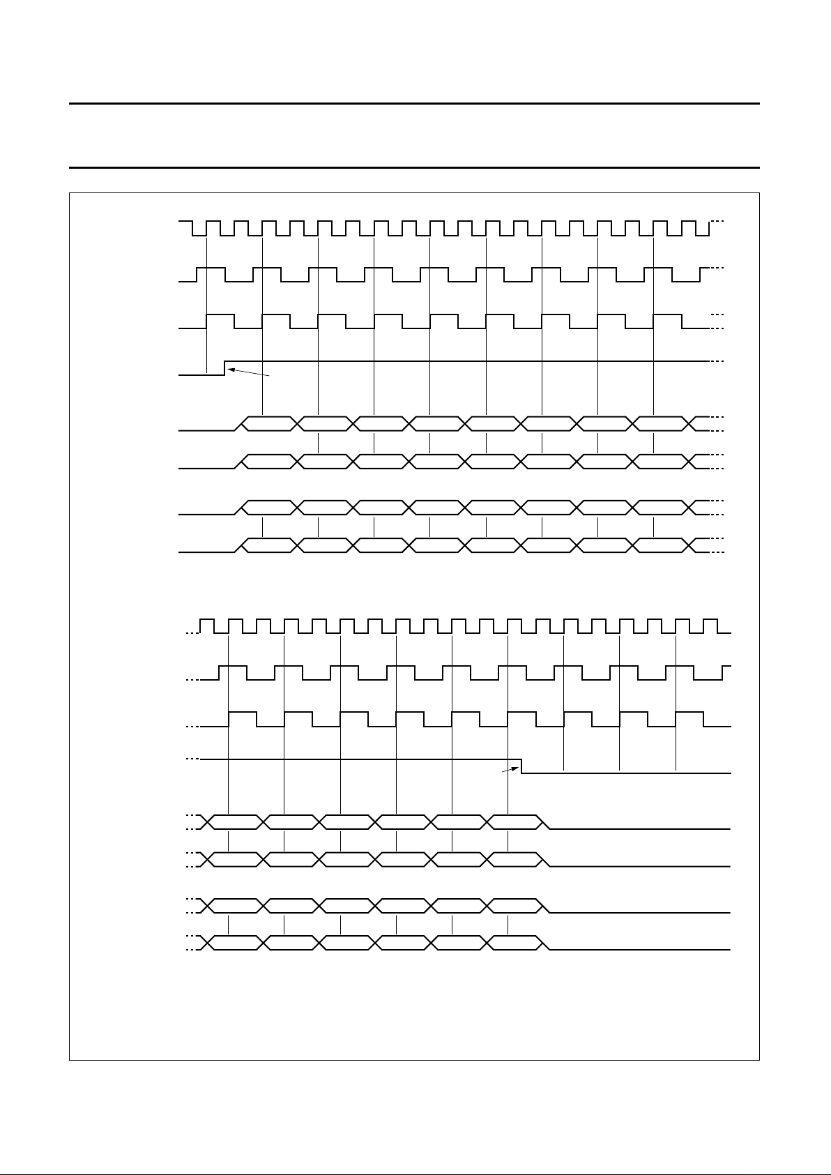
Fig.3 Line control by HREF for 4:2:2format, CREF = 13.5 MHz; HREF = 720 pixel; 50 and 60 Hz field.
handbook, full pagewidth
LL27
(LLC)
CREF
internal
bus clock
(LLC2)
HREF
start of
active line
0
U0
1
V0
2
U2
3
V2
4
U4
5
V4
6
U6
7
V6
Y signal
U and V signal
50 Hz
60 Hz
Byte number for pixels:
Y signal
U and V signal
MEH268
0
U0
1
V0
2
U2
3
V2
4
U4
5
V4
6
U6
7
V6
handbook, full pagewidth
LL27
(LLC)
CREF
internal
bus clock
(LLC2)
HREF
Y signal
U and V signal
end of
active line
714
V714
715
U716
716
V716
717
U718
718
V718
719
U714
50 Hz
MEH269
714
V714
715
U716
716
V716
717
U718
718
V718
719
U714
60 Hz
Byte number for pixels:
Y signal
U and V signal
a. Start of active line.
b. End of active line.

1996 Aug 20 9
Philips Semiconductors Product specification
Video Enhancement and Digital-to-Analog
processor (VEDA2)
SAA7165
Interpolation
The chrominance interpolation filter consists of various
filter stages, multiplexers and de-multiplexers to increase
the data rate of the colour-difference signals by a factor of
2 or 4. The switching of the filters by the bits IFF, IFC and
IFL is described previously. Additional signal samples with
significant amplitudes between two consecutive signal
samples of the low data rate are generated.
The time-multiplexed U and V samples are stored in
parallel for converting.
Data switch
The digital signals are adapted to the conversation range.
U and V data have 8-bit formats again; Y can have 9 bits
dependent on peaking. Blanking and switching to
colourless level is applied here. Bits can be inverted by
INV-bit to change the polarity of colour-difference output
signals.
Digital Colour Transient Improvement (DCTI)
The DCTI circuit improves the transition behaviour of the
UV colour-difference signals. As the CVBS signal allows
for a 4:1:1bandwidth representation only, the DCTI
improves the transients to the same performance as
signals coming from a 4 :2:2source, or even more.
In order to obtain the point of inflection, the second
derivative of the signal is calculated. The improved
transition is centred with respect to the point of inflection of
the original signal. Thus, there is no horizontal shift of the
resulting signal.
The transition area length to be improved is controlled via
I
2
C-bus by the bits LI1 and LI0 (Table 5); the sensitivity of
the DCTI block is controlled by the bits GA1 and GA0.
The CMO bit controls the colour detail sensitivity. It should
be set to logic 1 (ON) if the video signal contains fine
colour details (recommended operation mode).
Digital-to-Analog Converters (DACs)
Conversion is separate for Y, U and V. The converters use
resistor chains with low-impedance output buffers.
The minimum output voltage is 200 mV to reduce integral
non-linearity errors. The analog signal, without load on
output pin, is between 0.2 and 2.2 V floating.
An application for 1 V/75 Ω on outputs is shown in Fig.14.
Each digital-to-analog converter has its own supply and
ground pins suitable for decoupling. The reference
voltage, supplying the resistor chain of all three DACs, is
the supply voltage V
DDA4
. The current into pin 41 is
0.3 mA; a larger current improves the bandwidth but
increases the integral non-linearity.
I
2
C-bus format
Table 4 I
2
C-bus format; see notes 1 to 7
Notes
1. S = START condition.
2. Slave address = 1011 111X.
3. A = acknowledge; generated by the slave.
4. Subaddress = subaddress byte (Table 5);
If more than 1 byte of DATA is transmitted, then auto-increment of the subaddress is performed.
5. Data = data byte (Table 5).
6. P = STOP condition.
7. X = R/
W control bit:
a) X = 0; order to write (the circuit is slave receiver).
b) X = 1; order to read (the circuit is slave transmitter).
S slave address A subaddress A data 0 A ... data n A P
 Loading...