

Philips saa7167a DATASHEETS

INTEGRATED CIRCUITS
DATA SH EET
SAA7167A
YUV-to-RGB Digital-to-Analog
Converter DAC
Preliminary specification
File under Integrated Circuits, IC22
1996 Aug 14

Philips Semiconductors Preliminary specification
YUV-to-RGB Digital-to-Analog
Converter DAC
FEATURES
• On-chip mixing of digital video data and analog
RGB signals
• Supports video input format of YUV 4 :2:2, 4:1:1,
2:1:1 and RGB 5:6:5
• Video input rate up to 66 MHz
• Allows for both binary and two’s complement video
input data
• Triple 8-bit DACs for video output
• Built-in voltage output amplifier
• Provide keying control with external key and internal
8-bit, 2 × 8-bit and 3 × 8-bit pixel colour key
2
• Programmable via the I
• 5 V CMOS device; LQFP48 package.
GENERAL DESCRIPTION
The SAA7167A is a mixed-mode designed IC containing a
video data path, keying control block, analog mixer, and a
C-bus
SAA7167A
voltage output amplifier, capable of converting digital video
data to analog RGB video, and then mixing video and
external analog RGB inputs.
The video data path contains a data re-formatter,
YUV-to-RGB colour space matrix as well as triple DACs for
video data processing. An analog mixer performs
multiplexing between DAC outputs of the video path and
external analog RGB inputs.
The final analog outputs are buffered with built-in voltage
output amplifiers to provide the direct driving capability for
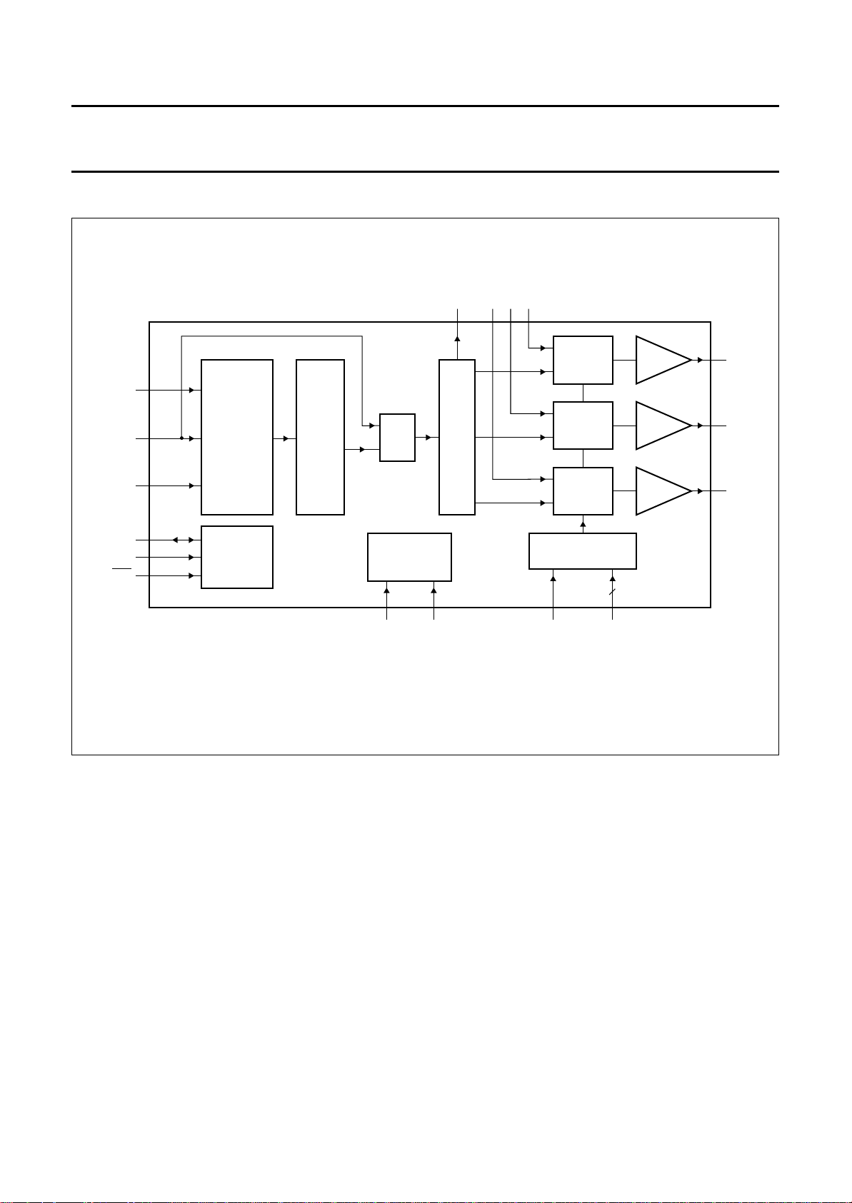
a 150 Ω load. Figure 1 shows the overall block diagram.
2
The operation of SAA7167 is controlled via the I
C-bus.
QUICK REFERENCE DATA
SYMBOL PARAMETER MIN. MAX. UNIT
V
DDD
V
DDA
T
amb
ORDERING INFORMATION
TYPE
NUMBER
SAA7167A LQFP48 plastic low profile quad flat package; 48 leads; body 7 × 7 × 1.4 mm SOT313-2
digital supply voltage 4.75 5.25 V
analog supply voltage 4.75 5.25 V
operating ambient temperature 0 70 °C
PACKAGE
NAME DESCRIPTION VERSION
1996 Aug 14 2
Philips Semiconductors Preliminary specification
YUV-to-RGB Digital-to-Analog
Converter DAC
BLOCK DIAGRAM
handbook, full pagewidth
YUV7 to
YUV0
UV7 to
UV0
HREF
SDA
SCL
RES
38 to
45
46 to 48,
1 to 5
9
22
23
24
RE-
FORMATTER
2
C-BUS
I
CONTROL
YUV
TO
RGB
MATRIX
SAA7167A
C
ref(h)
Bin Gin Rin
2936 31 33
MIXER
8-BIT
MUX
CLOCK
GENERATOR
VCLK PCLK EXTKEY P7 to P0
DAC
(3×)
MIXER
MIXER
KEYING CONTROL
8
13 to 2021106
SAA7167A
OPAMP
OPAMP
OPAMP
32
30
28
MBH532
Rout
Gout
Bout
Fig.1 Block diagram.
1996 Aug 14 3

Philips Semiconductors Preliminary specification
YUV-to-RGB Digital-to-Analog
SAA7167A
Converter DAC
PINNING
SYMBOL PIN DESCRIPTION I/O
UV4 1 digital video UV (of YUV format 4:1:1 and 4:2:2) input data, or digital G and R
input data
UV3 2 digital video UV (of YUV format 4:1:1 and 4:2:2) input data, or digital G and R
input data
UV2 3 digital video UV (of YUV format 4:1:1 and 4:2:2) input data, or digital G and R
input data
UV1 4 digital video UV (of YUV format 4:1:1 and 4:2:2) input data, or digital G and R
input data
UV0 5 digital video UV (of YUV format 4:1:1 and 4:2:2) input data, or digital G and R
input data
VCLK 6 video clock input I
V
DDD
V
SSD
HREF 9 horizontal reference input signal I
PCLK 10 pixel clock input I
AP 11 test pins, normally connected to ground I
SP 12 test pins, normally connected to ground I
P7 13 pixel bus input 7 (for keying control) I
P6 14 pixel bus input 6 (for keying control) I
P5 15 pixel bus input 5 (for keying control) I
P4 16 pixel bus input 4 (for keying control) I
P3 17 pixel bus input 3 (for keying control) I
P2 18 pixel bus input 2 (for keying control) I
P1 19 pixel bus input 1 (for keying control) I
P0 20 pixel bus input 0 (for keying control) I
EXTKEY 21 external key signal input I
SDA 22 I
SCL 23 I
RES 24 set to LOW to reset the I2C-bus I
n.c. 25 not connected −
V
SSA2
V
DDA2
Bout 28 analog Blue signal output O
Bin 29 analog Blue signal input I
Gout 30 analog Green signal output O
Gin 31 analog Green signal input I
Rout 32 analog Red signal output O
Rin 33 analog Red signal input I
V
SSA1
V
DDA1
C
ref(h)
7 digital supply voltage I/O
8 digital ground I/O
2
C-bus data line I/O
2
C-bus clock line I
26 analog ground 2 I/O
27 analog supply voltage 2 I/O
34 analog ground 1 I/O
35 analog supply voltage 1 I/O
36 capacitor for reference high voltage output (2.25 V) I/O
I
I
I
I
I
1996 Aug 14 4

Philips Semiconductors Preliminary specification
YUV-to-RGB Digital-to-Analog
SAA7167A
Converter DAC
SYMBOL PIN DESCRIPTION I/O
n.c. 37 not connected −
YUV7 38 digital video Y or UV (of YUV format 2:1:1) input data, or digital G and B input data I
YUV6 39 digital video Y or UV (of YUV format 2:1:1) input data, or digital G and B input data I
YUV5 40 digital video Y or UV (of YUV format 2:1:1) input data, or digital G and B input data I
YUV4 41 digital video Y or UV (of YUV format 2:1:1) input data, or digital G and B input data I
YUV3 42 digital video Y or UV (of YUV format 2:1:1) input data, or digital G and B input data I
YUV2 43 digital video Y or UV (of YUV format 2:1:1) input data, or digital G and B input data I
YUV1 44 digital video Y or UV (of YUV format 2:1:1) input data, or digital G and B input data I
YUV0 45 digital video Y or UV (of YUV format 2:1:1) input data, or digital G and B input data I
UV7 46 digital video UV (of YUV format 4:1:1 and 4:2:2) input data, or digital G and R
input data
UV6 47 digital video UV (of YUV format 4:1:1 and 4:2:2) input data, or digital G and R
input data
UV5 48 digital video UV (of YUV format 4:1:1 and 4:2:2) input data, or digital G and R
input data
I
I
I
UV4
UV3
UV2
UV1
UV0
VCLK
V
DDD
V
SSD
HREF
PCLK
index
corner
AP
SP
UV7
UV6
47
14
P6
46
15
P5
YUV0
YUV1
45
44
SAA7167A
16
17
P4
P3
UV5
48
1
2
3
4
5
6
7
8
9
10
11
12
13
P7
YUV2
43
18
P2
YUV3
42
19
P1
YUV4
41
20
P0
YUV5
YUV6
40
39
21
22
SDA
EXTKEY
YUV7
38
23
SCL
n.c.
24 37
RES
36
35
34
33
32
31
30
29
28
27
26
25
MBH531
C
ref(h)
V
DDA1
V
SSA1
Rin
Rout
Gin
Gout
Bin
Bout
V
DDA2
V
SSA2
n.c.
1996 Aug 14 5
Fig.2 Pin configuration.

Philips Semiconductors Preliminary specification
YUV-to-RGB Digital-to-Analog
Converter DAC
FUNCTIONAL DESCRIPTION
The SAA7167A contains a video data path, 3 analog
mixers and voltage output amplifiers for the RGB channels
respectively, a keying control block as well as an I2C-bus
control block.
Video data path
The video data path includes a video data re-formatter, a
YUV-to-RGB colour space conversion matrix, and triple
8-bit DACs.
E-FORMATTER
R
The re-formatter de-multiplexes the different video formats
YUV 4 :1:1, 4:2:2 or 2:1:1 to internal YUV 4 : 4 : 4,
which can then be processed by the RGB matrix. The pixel
byte sequences of those video input formats are shown in
Tables 1 to 4.
Table 1 Pixel byte sequence of 4 :2:2
INPUT
YUV0 (LSB)
YUV1
YUV2
YUV3
YUV4
YUV5
YUV6
YUV7 (MSB)
UV0 (LSB)
UV1
UV2
UV3
UV4
UV5
UV6
UV7 (MSB)
Y data
UV data
PIXEL BYTE SEQUENCE OF
4:2:2
Y0 Y0 Y0 Y0 Y0 Y0
Y1 Y1 Y1 Y1 Y1 Y1
Y2 Y2 Y2 Y2 Y2 Y2
Y3 Y3 Y3 Y3 Y3 Y3
Y4 Y4 Y4 Y4 Y4 Y4
Y5 Y5 Y5 Y5 Y5 Y5
Y6 Y6 Y6 Y6 Y6 Y6
Y7 Y7 Y7 Y7 Y7 Y7
U0 V0 U0 V0 U0 V0
U1 V1 U1 V1 U1 V1
U2 V2 U2 V2 U2 V2
U3 V3 U3 V3 U3 V3
U4 V4 U4 V4 U4 V4
U5 V5 U5 V5 U5 V5
U6 V6 U6 V6 U6 V6
U7 V7 U7 V7 U7 V7
012345
024
SAA7167A
Table 2 Pixel byte sequence of 4:1:1
INPUT PIXEL BYTE SEQUENCE OF 4:1:1
YUV0
YUV1
YUV2
YUV3
YUV4
YUV5
YUV6
YUV7
UV0
UV1
UV2
UV3
UV4
UV5
UV6
UV7
Y data
UV data
Table 3 Pixel byte sequence of 2:1:1
INPUT PIXEL BYTE SEQUENCE OF 2:1:1
YUV0
YUV1
YUV2
YUV3
YUV4
YUV5
YUV6
YUV7
Y data
UV data
Y0 Y0 Y0 Y0 Y0 Y0 Y0 Y0
Y1 Y1 Y1 Y1 Y1 Y1 Y1 Y1
Y2 Y2 Y2 Y2 Y2 Y2 Y2 Y2
Y3 Y3 Y3 Y3 Y3 Y3 Y3 Y3
Y4 Y4 Y4 Y4 Y4 Y4 Y4 Y4
Y5 Y5 Y5 Y5 Y5 Y5 Y5 Y5
Y6 Y6 Y6 Y6 Y6 Y6 Y6 Y6
Y7 Y7 Y7 Y7 Y7 Y7 Y7 Y7
XXXXXXXX
XXXXXXXX
XXXXXXXX
XXXXXXXX
V6 V4 V2 V0 V6 V4 V2 V0
V7 V5 V3 V1 V7 V5 V3 V1
U6 U4 U2 U0 U6 U4 U2 U0
U7 U5 U3 U1 U7 U5 U3 U1
01234567
04
U0 Y0 V0 Y0 U0 Y0 V0 Y0
U1 Y1 V1 Y1 U1 Y1 V1 Y1
U2 Y2 V2 Y2 U2 Y2 V2 Y2
U3 Y3 V3 Y3 U3 Y3 V3 Y3
U4 Y4 V4 Y4 U4 Y4 V4 Y4
U5 Y5 V5 Y5 U5 Y5 V5 Y5
U6 Y6 V6 Y6 U6 Y6 V6 Y6
U7 Y7 V7 Y7 U7 Y7 V7 Y7
X0X2X4X6
0X0X4X4X
1996 Aug 14 6
 Loading...