

Philips saa7158 DATASHEETS
INTEGRATED CIRCUITS
DATA SH EET
SAA7158
Back END IC
Preliminary specification
File under Integrated Circuits, IC02
July 1994
Philips Semiconductors Preliminary specification
Back END IC SAA7158
FEATURES
• Line Flicker Reduction (LFR) by means of MEDIAN filtering
• Vertical zoom
• Digital colour transient improvement
• Digital luminance peaking
• Movie phase detection
• 4:4:4 YUV data throughput selectable, standard is 4:1:1 Y/U/V
• D/A conversion
• UART interface.
GENERAL DESCRIPTION
Application Environment
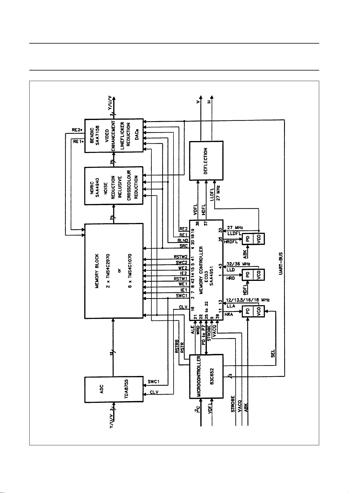
The Back END IC (abbreviated as BENDIC) is designed to cooperate with an 8051 type of microprocessor, the ECO3
(SAA4951) memory controller and Texas Instruments TMS4C2970 memories, but other configurations may be
applicable. Fig.1 shows the block diagram of the feature box. The nominal clock frequency of the IC is 27 MHz or 32 MHz,
with a maximum of 36 MHz.
The system supports the digital Y/U/V bus for selection of different video signal sources. The Y/U/V bus and the BENDIC
data input are fully synchronous with respect to the clock signal. A line reference signal BLN for timing control purposes
has to be provided by external elements which always controls the system timing, independent of active signal sources
or desired functions.
Analog Characteristics
The BENDIC contains 3 independent, high speed digital to analog converters for luminance and colour difference signal
processing and conversion. The resolution of the two DA converters for the colour difference signals is 8 bit. The
luminance peaking up to 6 dB at high frequencies widens the resolution of the luminance channel. To avoid aliasing
effects due to time discrete amplitude limiting the resolution of 9-bit is offered for the luminance conversion. All output
stages provide high performance output stages for driving lines with low impedance line termination.
QUICK REFERENCE DATA
SYMBOL PARAMETER MIN. MAX. UNIT
V
DD
digital supply voltage 4.5 5.5 V
analog supply voltage 4.75 5.25 V
T
amb
operating ambient temperature 0 +70 °C
ORDERING INFORMATION
EXTENDED
TYPE NUMBER
PINS PIN POSITION MATERIAL CODE
SAA7158WP 68 PLCC plastic SOT188
PACKAGE
(1)
Note
1. SOT188-2; 1996 November 26.
July 1994 2
Philips Semiconductors Preliminary specification
Back END IC SAA7158
July 1994 3
Fig.1 Block diagram of the feature box.
Philips Semiconductors Preliminary specification
Back END IC SAA7158
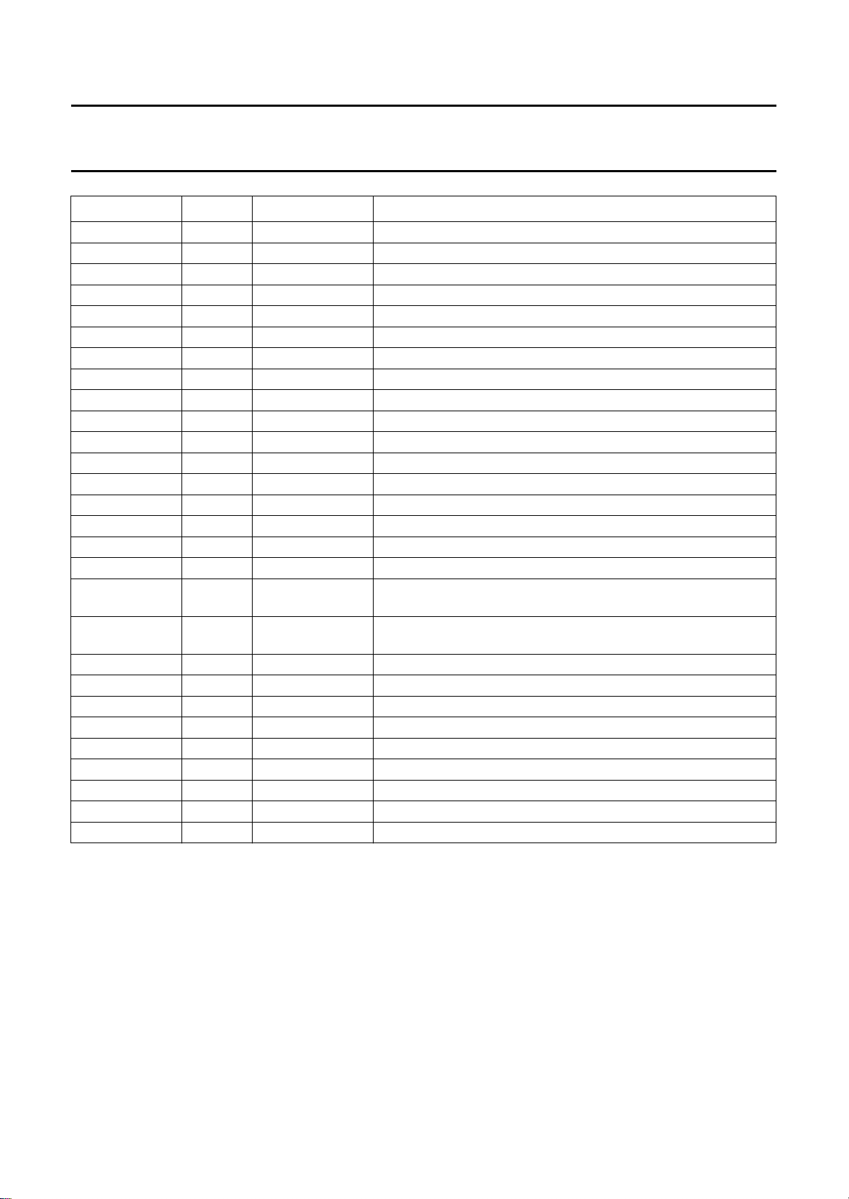
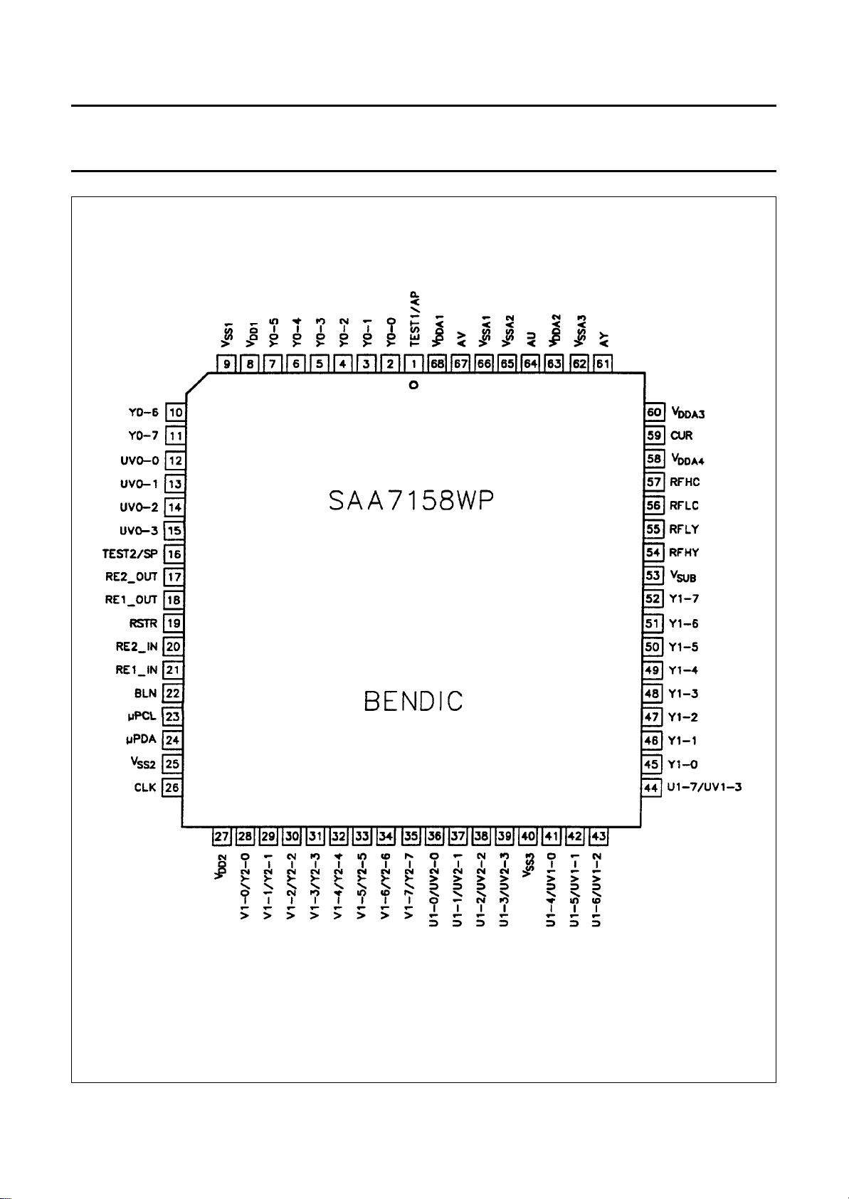
PINNING
SYMBOL PIN TYPE DESCRIPTION
TEST1/AP 1 input action pin for testing; to be connected to V
Y0-0 2 3-state output feedback_data to second memory, Y bit 0
Y0-1 3 3-state output feedback_data to second memory, Y bit 1
Y0-2 4 3-state output feedback_data to second memory, Y bit 2
Y0-3 5 3-state output feedback_data to second memory, Y bit 3
Y0-4 6 3-state output feedback_data to second memory, Y bit 4
Y0-5 7 3-state output feedback_data to second memory, Y bit 5
V
DD1
V
SS1
8 supply positive digital supply voltage (+5 V)
9 ground digital ground
Y0-6 10 3-state output feedback_data to second memory, Y bit 6
Y0-7 11 3-state output feedback_data to second memory, Y bit 7
UV0-0 12 3-state output feedback_data to second memory, UV bit 0
UV0-1 13 3-state output feedback_data to second memory, UV bit 1
UV0-2 14 3-state output feedback_data to second memory, UV bit 2
UV0-3 15 3-state output feedback_data to second memory, UV bit 3
TEST2/SP 16 input shift pin for testing; to be connected to V
RE2_OUT 17 output redirected read enable to memory 2
RE1_OUT 18 output redirected read enable to memory 1
RSTR 19 input memory read, µP interface and movie detection reset
RE2_IN 20 input input for read enable to memory 2
RE1_IN 21 input input for read enable to memory 1
BLN 22 input blanking signal
µPCL 23 input clock for interface with 8051 UART, mode 0
µPDA 24 in/output data for interface with 8051 UART, mode 0
V
SS2
25 ground digital ground
CLK 26 input master clock, nominal 27 (32) MHz
V
DD2
27 supply positive digital supply voltage (+5 V)
V1-0/Y2-0 28 input V data, bit 0 in 4:4:4; Y data second memory, bit 0
V1-1/Y2-1 29 input V data, bit 1 in 4:4:4; Y data second memory, bit 1
V1-2/Y2-2 30 input V data, bit 2 in 4:4:4; Y data second memory, bit 2
V1-3/Y2-3 31 input V data, bit 3 in 4:4:4; Y data second memory, bit 3
V1-4/Y2-4 32 input V data, bit 4 in 4:4:4; Y data second memory, bit 4
V1-5/Y2-5 33 input V data, bit 5 in 4:4:4; Y data second memory, bit 5
V1-6/Y2-6 34 input V data, bit 6 in 4:4:4; Y data second memory, bit 6
V1-7/Y2-7 35 input V data, bit 7 in 4:4:4; Y data second memory, bit 7
U1-0/UV2-0 36 input U data, bit 0 in 4:4:4; UV data second memory, bit 0
U1-1/UV2-1 37 input U data, bit 1 in 4:4:4; UV data second memory, bit 1
U1-2/UV2-2 38 input U data, bit 2 in 4:4:4; UV data second memory, bit 2
U1-3/UV2-3 39 input U data, bit 3 in 4:4:4; UV data second memory, bit 3
V
SS3
40 ground digital ground
SS
SS
July 1994 4
Philips Semiconductors Preliminary specification
Back END IC SAA7158
SYMBOL PIN TYPE DESCRIPTION
U1-4/UV1-0 41 input U data, bit 4 in 4:4:4; UV data first memory, bit 0
U1-5/UV1-1 42 input U data, bit 5 in 4:4:4; UV data first memory, bit 1
U1-6/UV1-2 43 input U data, bit 6 in 4:4:4; UV data first memory, bit 2
U1-7/UV1-3 44 input U data, bit 7 in 4:4:4; UV data first memory, bit 3
Y1-0 45 input Y data first memory, bit 0
Y1-1 46 input Y data first memory, bit 1
Y1-2 47 input Y data first memory, bit 2
Y1-3 48 input Y data first memory, bit 3
Y1-4 49 input Y data first memory, bit 4
Y1-5 50 input Y data first memory, bit 5
Y1-6 51 input Y data first memory, bit 6
Y1-7 52 input Y data first memory, bit 7
V
SUB
53 analog ground substrate pin; connect to analog ground (V
RFHY 54 analog input connect C = 100 nF to analog ground (V
RFLY 55 analog input connect to analog ground (V
RFLC 56 analog input connect to analog ground (V
SSA
SSA
)
)
RFHC 57 analog input connect C = 100 nF to analog ground (V
V
DDA4
58 analog supply analog supply voltage for reference ladders of the three DA
converters and for current sources of the output buffers
CUR 59 analog input current input for analog output buffers (0.4 mA from V
connect with R = 15 kΩ
V
DDA3
60 analog supply analog supply voltage for output buffer AY
AY 61 analog output analog luminance Y output
V
V
SSA3
DDA2
62 analog ground analog ground for output buffer AY
63 analog supply analog supply voltage for output buffer AU
AU 64 analog output analog (B-Y) or −(B-Y) output
V
V
SSA2
SSA1
65 analog ground analog ground for output buffer AU
66 analog ground analog ground for output buffer AV
AV 67 analog output analog (R-Y) or −(R-Y) output
V
DDA1
68 supply analog supply voltage for output buffer AV
SSA
SSA
SSA
)
)
)
= 5 V);
DDA4
July 1994 5
Philips Semiconductors Preliminary specification
Back END IC SAA7158
July 1994 6
Fig.2 Pin configuration.
 Loading...