


INTEGRATED CIRCUITS
DATA SH EET
SAA7151B
Digital multistandard colour
decoder with SCART interface
(DMSD2-SCART)
Product specification
File under Integrated Circuits, IC02
April 1993

Philips Semiconductors Product specification
Digital multistandard colour decoder
with SCART interface (DMSD2-SCART)
FEATURES
• 8-bit performance on chip for luminance and
chrominance signal processing for PAL, NTSC and
SECAM standards
• Separate 8-bit luminance and 8-bit chrominance input
signals from Y/C, CVBS, S-Video (S-VHS or Hi8)
sources
• SCART signal insertion by means of RGB/YUV
convertion; fast switch handling
• Horizontal and vertical sync detection for all standards
• Real time control output RTCO
• Fast sync recovery of vertical blanking for VCR signals
(bottom flutter compensation)
• Controls via the I2C-bus
• User programmable aperture correction (horizontal
peaking)
• Cross-colour reduction by chrominance comb-filtering
(NTSC) or by special cross-colour cancellation
(SECAM)
• 8-bit quantization of output signals in 4:1:1 or 4:2:2
formats
• 720 active samples per line
SAA7151B
• The YUV bus supports a data rate of 13.5 MHz
(CCIR 601).
– (864 × f
– (858 × fH) for 60 Hz
• Compatible with memory-based features (line-locked
clock)
• One 24.576 MHz crystal oscillator for all standards
GENERAL DESCRIPTION
The SAA7151B is a digital multistandard colour-decoder
having two 8-bit input channels, one for CVBS or Y, the
other for chrominance or time-multiplexed
colour-difference signals.
) for 50 Hz
H
QUICK REFERENCE DATA
SYMBOL PARAMETER MIN. TYP. MAX. UNIT
V
DD
I
DD
V
I
V
O
T
amb
supply voltage (pins 5, 18, 28, 37 and 52) 4.5 5 5.5 V
total supply current (pins 5, 18, 28, 37 and 52) − 100 250 mA
input levels TTL-compatible
output levels TTL-compatible
operating ambient temperature 0 − 70 °C
ORDERING INFORMATION
EXTENDED TYPE
NUMBER
PINS PIN POSITION MATERIAL CODE
PACKAGE
SAA7151B 68 mini-pack PLCC plastic SOT188
Note
1. SOT188-2; 1996 December 16.
(1)
April 1993 2
Philips Semiconductors Product specification
Digital multistandard colour decoder with
SCART interface (DMSD2-SCART)
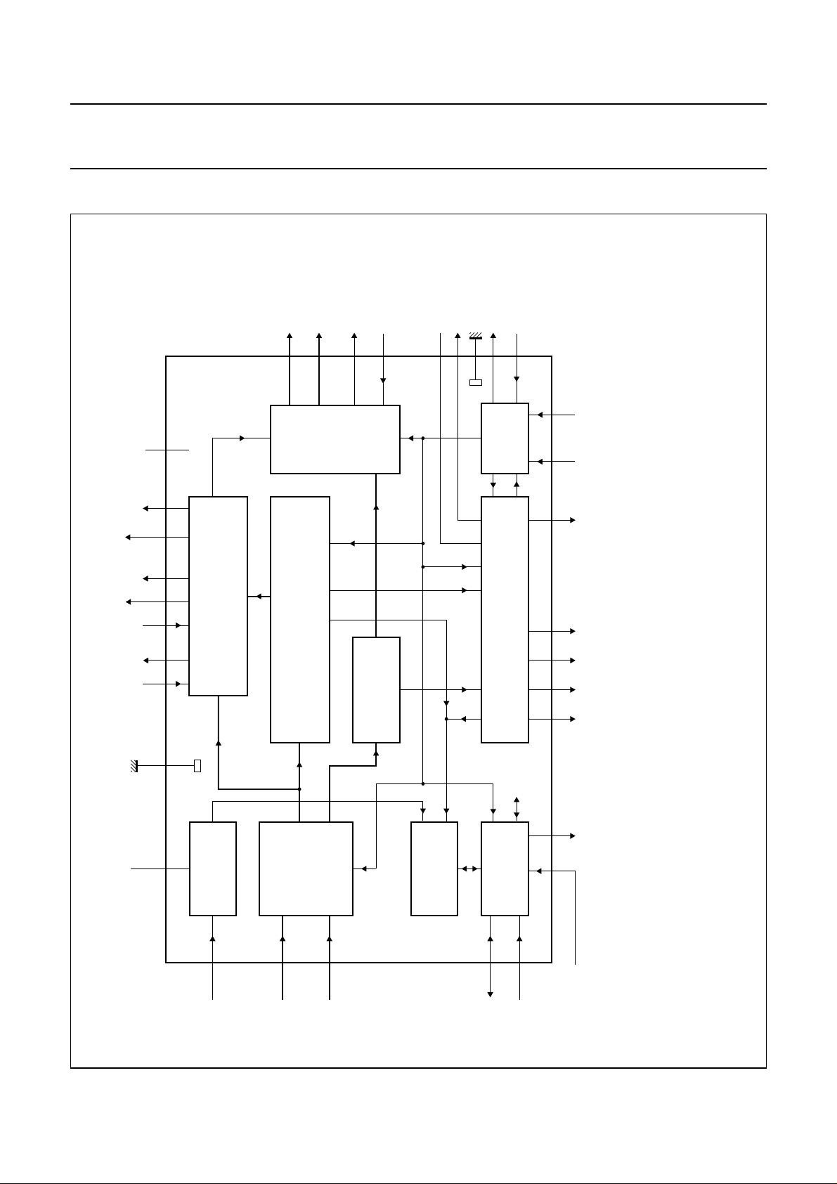
BLOCK DIAGRAM
FEIN
HREF
UV output
(UV7 to UV0)
Y output
(Y7 to Y0)
42
64
53, 54
55 to 62
45 to 50,
1, 2
test pins
GPSW2SYIS
OUTPUT
INTERFACE
DDA
LFCO
V
+5 V
373635
SSA
V
33
XTAL
CLOCK
XTALI
34
SAA7151B
MEH292
39 4 27
ll pagewidth
GPSW1MUXC
CPI
FSO
SCART
FSI
+5 V
44 65 32 24 25
68 66
SS4
to V
SS1
V
DD4
to V
DD1
V
5, 18, 28, 52 19, 38, 51, 67
FAST SWITCH INSERTION
COMPONENT PROCESSING;
SCART INTERFACE CONTROL;
CHROMINANCE PROCESSOR
SAA7151A
14 to 17
20 to 23
CVBS7
CVBS0 to
INPUT
INTERFACE
6 to 13
CUV7
CUV0 to
RESET
POWER-ON
3
RESN
LUMINANCE
PROCESSOR
clock
status
STATUS
REGISTER
SYNCHRONIZATION
C-BUS
2
I
CONTROL
41
40
SCL
SDA
HSY VS HS ODD CREF LL27
Fig.1 Block diagram (application circuits see Figs 17, 18 and 19).
GPSW0 HCL
43 63 26 29 30 31
IICSA
April 1993 3

Philips Semiconductors Product specification
Digital multistandard colour decoder with
SAA7151B
SCART interface (DMSD2-SCART)
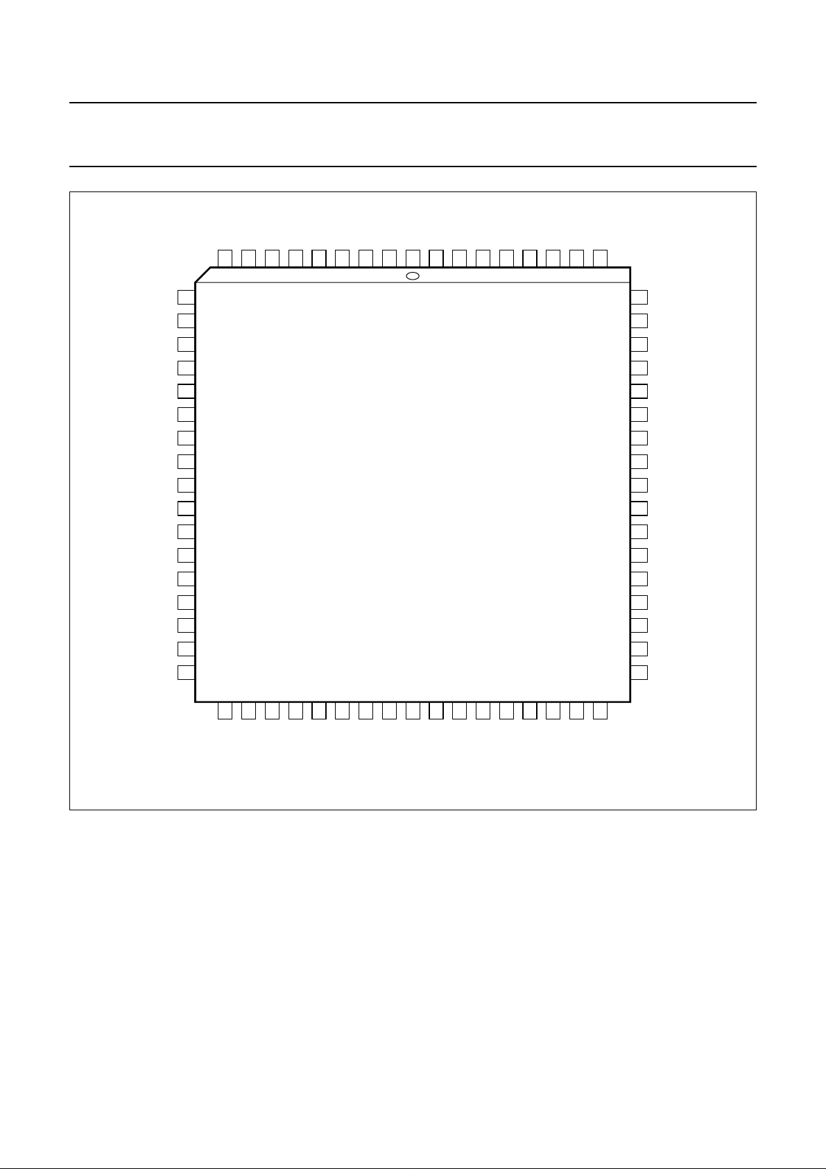
PINNING
SYMBOL PIN DESCRIPTION
SP 1 connected to ground (shift pin for testing)
AP 2 connected to ground (action pin for testing)
RESN 3 reset, active-LOW
CREF 4 clock reference, sync from external to ensure in-phase signals on the Y-, CUV- and YUV-bus
V
DD1
CUV0 6
CUV1 7
CUV2 8
CUV3 9
CUV4 10
CUV5 11
CUV6 12
CUV7 13
CVBS0 14
CVBS1 15
CVBS2 16
CVBS3 17
V
DD2
V
SS1
CVBS4 20
CVBS5 21
CVBS6 22
CVBS7 23
GPSW1 24 status bit output FSST0 or port 1 output for general purpose (programmable by subaddress 0C)
GPSW2 25 status bit output FSST1 or port 2 output for general purpose (programmable by subaddress 0C)
HCL 26 black level clamp pulse output (begin and stop programmable), e.g. for TDA8708A (ADC)
LL27 27 line-locked system clock input signal (27 MHz)
V
DD3
HSY 29 hor. sync pulse reference output (begin and stop programmable), e.g. for gain adj.TDA8708A
VS 30 vertical sync output signal (Fig.11)
HS 31 horizontal sync output signal (Fig.16; start point programmable)
RTCO 32 real time control output; serial increments of HPLL and FSCPLL and status PAL or SECAM
XTAL 33 24.576 MHz clock output (open-circuit for use with external oscillator)
XTALI 34 24.576 MHz connection for crystal or external oscillator (TTL compatible squarewave)
V
SSA
LFCO 36 line frequency control output signal, multiple of horizontal frequency (nominal 6.75 MHz)
V
DDA
V
SS2
5 +5 V supply input 1
chrominance input data bits CUV7 to CUV0 (digitized chrominance signals in two’s complement
format from a S-Video source (S-VHS, Hi8) or time-multiplexed colour-difference signals from a
YUV(RGB) source or both in combination)
CVBS lower input data bits CVBS3 to CVBS0
(CVBS with luminance, chrominance and all sync information in two’s complement format)
18 +5 V supply input 2
19 ground 1 (0 V)
CVBS upper input data bits CVBS7 to CVBS4
(CVBS with luminance, chrominance and all sync information in two’s complement format)
28 +5 V supply input 3
(ADC)
sequence (Fig.10)
35 analog ground
37 +5 V supply input for analog part
38 ground 2 (0 V)
April 1993 4

Philips Semiconductors Product specification
Digital multistandard colour decoder with
SAA7151B
SCART interface (DMSD2-SCART)
SYMBOL PIN DESCRIPTION
ODD 39 odd/even field identification output (odd = HIGH)
SDA 40 I
SCL 41 I
HREF 42 horizontal reference for YUV data outputs (for active line 720Y samples long)
IICSA 43 set module address input of I
CPI 44 clamping pulse input (digital clamping of external UV signals)
Y7 45
Y6 46
Y5 47
Y4 48
Y3 49
Y2 50
V
SS3
V
DD4
Y1 53
Y0 54
UV7 55
UV6 56
UV5 57
UV4 58
UV3 59
UV2 60
UV1 61
UV0 62
GPSW0 63 port output for general purpose (programmable by subaddress 0D)
FEIN 64 fast enable input (active-LOW to control fast switching due to YUV data; HIGH = YUV high-Z
MUXC 65 multiplexer control output; source select signal for external ADC (UV signal multiplexing)
FSO 66 fast switch and sync insertion output; gated FS signal from FSI or sync insertion pulse in full screen
V
SS4
FSI 68 fast switch input signal fed from SCART/peri-TV connector (indicates fast insertion of RGB signals)
2
C-bus data line
2
C-bus clock line
Y signal output bits Y7 to Y2 (luminance), part of the digital YUV-bus
51 ground 3 (0 V)
52 +5 V supply input 4
Y signal output bits Y1 to Y0 (luminance), part of the digital YUV-bus
UV signal output bits UV7 to UV0, part of the digital YUV-bus
RGB mode
67 ground 4 (0 V)
2
C-bus (LOW = 1000 101X; HIGH = 1000 111X)
April 1993 5
Philips Semiconductors Product specification
Digital multistandard colour decoder with
SCART interface (DMSD2-SCART)
handbook, full pagewidth
CUV0
6
DD1
V
5
CREF
RESNAPSP
4
3
2
SAA7151A
SAA7151B
CUV4
CUV5
CUV6
CUV7
CVBS0
CVBS1
CVBS2
CVBS3
V
DD2
V
SS1
CVBS4
CVBS5
CVBS6
CVBS7
GPSW1
GPSW2
HCL
CUV3
CUV2
CUV1
9
8
7
10
11
12
13
14
15
16
17
18
19
20
21
22
23
24
25
26
SAA7151B
SS4
FSI
V
FSO
MUXC
FEIN
GPSW0
UV0
UV1
1
68
67
66
65
64
63
62
61
60
UV2
59
UV3
58
UV4
57
UV5
56
UV6
55
UV7
54
Y0
53
Y1
52
V
DD4
51
V
SS3
Y2
50
49
Y3
48
Y4
47
Y5
46
Y6
45
Y7
44
CPI
27
28
29
30
31
32
33
34
VS
LL27
DD3
V
HSY
HS
SYIS
XTAL
XTALI
Fig.2 Pin configuration.
FUNCTIONAL DESCRIPTION
System configuration
The SAA7151B system processes digital TV signals with
line-locked clock in PAL, SECAM and NTSC standards
(CVBS or S-Video) as well as RGB signals coming from a
SCART/peri-TV connector. The different source signals
are switched, if necessary matrixed and converted (Fig.3
and Table 1).
8-bit CVBS data (digitized composite video) and 8-bit UV
data (digitized chrominance and /or time-multiplexed
colour-difference signals) are fed to the SAA7151B. The
data rate is 27 MHz.
April 1993 6
35
36
37
38
39
40
41
42
43
SSA
V
LFCO
DDA
V
SS2
V
ODD
SDA
SCL
HREF
MEH293
IICSA
Chrominance processing
The 8-bit chrominance input signal (signal “C” out of CVBS
or Y/C in Fig.4) is fed via the input interface to a bandpass
filter for eliminating the DC component, then to the
quadrature demodulator. Subcarrier signals from the local
oscillator (DTO1) with 90 degree phase shift are applied to
its multiplier inputs. The frequency depends on set TV
standard.

Philips Semiconductors Product specification
Digital multistandard colour decoder with
SCART interface (DMSD2-SCART)
handbook, full pagewidth
C
TDA8446
VIDEO
SWITCH AND
MATRIX
SW1
SW2
SCART
CVBS
Y/C
R
G
B
sync
(PERI-TV)
FS
C
Y
2
I C-bus
(select)
TDA8540
VIDEO
SWITCH
CVBS/Y
sync
chroma
CVBS/Y/sync
BP
C
R
G
B
sync
CPI
HCL
FS
*
FSO
U
CSO
CPO
+
V2
U/V
HCT4053
MULTIPLEXER
LP
LP
V
GPSW1
LP
Y
V0
AO
ADI
TDA8709A
8-bit ADC
and multiplexer
(CHROMINANCE)
S0
S1
FE
CLS
CLP
+5 V
from SCART interface SAA7151B
AO
TDA8708A
ADI
8-bit ADC
(LUMINANCE)
GA
GB
SAA7151B
CUV(7-0)
DO(7-0)
CLK
MUXC
clamping
CPI
FSI
CVBS(7-0)
DO(7-0)
CLK
to and from SAA7151B
* fast switching of Y signal for insertion
(UV are switched inside SAA7151B)
Fig.3 System configuration, RGB fast switch interface included (SCART).
The multipliers operate as a quadrature demodulator for all
PAL and NTSC signals; it operates as a frequency
down-mixer for SECAM signals.
The two multiplier output signals are converted to a serial
UV data stream and applied to two low-pass filter stages,
then to a gain controlled amplifier. A final multiplexed
low-pass filter achieves, together with the preceding
stages, the required bandwidth performance. The from
PAL and NTSC originated signals are applied to a
comb-filter. The signals, originated from SECAM, are fed
through a cloche filter (0 Hz centre frequency), a phase
demodulator and a differentiator to obtain
frequency-demodulated colour-difference signals.
The SECAM signals are fed after de-emphasis to a
cross-over switch, to provide the both serial-transmitted
colour-difference signals. These signals are finally fed via
GPSW2
GPSW1
MEH305-3
the fast switch to the output formatter stages and to the
output interface.
Chrominance signals are output in parallel (4:2:2) on the
YUV-bus. The data rate of Y signal (pixel rate) is
13.5 MHz. UV signals have a data rate of 13.5 MHz/2 for
the 4:2.2 format (Table 2) respectively 13.5 MHz/4 for the
4:1.1 format (Table 3).
Component processing and SCART interface control
The 8-bit multiplexed colour-difference input signal (signal
CUV, Fig.1, out of matrixed RGB in Fig.3) is fed via the
input interface to a chrominance stop filter (UV signal only
can pass through; Figures 22 to 24). Here it is clamped
and fed to the offset compensation which can be enabled
or disabled via the I
2
C-bus.
April 1993 7
Philips Semiconductors Product specification
Digital multistandard colour decoder with
SCART interface (DMSD2-SCART)
For matrixed RGB signals - the full screen SCART mode
and the fast insertion mode (blanking/switching) are
selectable. The chrominance stop filter is automatically
bypassed in full screen SCART mode.
Full screen RGB mode (SCART):
The CUV digital input signal (7-0) consists of
time-multiplexed samples for U and V. An offset correction
for both signals is applied to correct external clamping
Table 1 SCART interface control (Fig.3)
MODE CONNECTION chroma
output of
FSO GPSW 2 GPSW 1 MUXC
RGB
only
Y/C or
CVBS
only
Fast
switch00
RGB
only
Fast
switch11
0
0
0
0
0
0
1
1
1
1
1
1
0
0
0
0
1
1
1
1
0
0
0
0
1
1
1
1
0
0
1
1
0
0
1
1
0
0
1
1
0
0
1
1
TDA8446
to TDA8709A
0
high-Z VIN2 U/V sync (RGB) sync (RGB)
1
0
C VIN1 C Y (Y/C) or CVBS
1
0
C VIN2
1
0
1
0
high-Z VIN2 U/V Y (RGB) sync (RGB)
1
0
1
0
C VIN2
1
0
1
SAA7151B
errors. An internal timing correction compensates for slight
differences in timing during sampling. The U and V signals
are delay-compensated and fed to the output formatter.
The format 4:2:2 or 4:1:1 is generated by a switchable
filter.
The control signals for the front end (Figures 3 and 20)
MUXC, status bits FSST1, FSST0 (outputs GPSW2,
GPSW1) and FSO are generated by the SAA7151B.
TDA8709A
selected
input
CUV
(7-0)
0.5(C+U)/
0.5(C+V)
0.5(C+U)/
0.5(C+V)
luminance
fast switch
TDA8446
Y (Y/C) or CVBS
not used
not used
Y (RGB)
not used
input
selector (via
2
I
C-bus)
TDA8540
Y (Y/C) or
CVBS
Y (Y/C) or
CVBS
Y (Y/C) or
CVBS
Fast insertion mode:
Fast insertion is applied by FSI pulse to ensure correct
timing. The RGB source signal is matrixed into UV and
inserted into the CVBS or Y/C source signal after two field
periods if FSI pulses are received. The output FSO is set
to HIGH during a determined insertion window (screen
plain minus 6 % of horizontal and vertical deflection).
Switch over depends on the phase of FSI in relation to the
valid pixel sequence depending on the phase-different
weighting factors. They are applied to the original and the
April 1993 8
inserted UV data (Figures 6 and 7)
The control signals for the front end (Table 1) MUXC, FSO,
status bits FSST1 and FSST0 (outputs GPSW2 and
GPSW1) are generated by the SAA7151B.
The amplitude of chrominance and colour-difference
signals are scaled down by factor 2 to avoid overloading of
the chrominance analog-to-digital converter. The
amplitudes are reduced in the TDA8446 by signals on lines
GPSW2 and GPSW1.

Philips Semiconductors Product specification
Digital multistandard colour decoder with
SCART interface (DMSD2-SCART)
Luminance processing
The luminance input signal, a digital CVBS format or an
8-bit luminance format (S-Video), is fed through a sample
rate converter to reduce the data rate to 13.5 MHz (Fig.5).
Sample rate is converted by means of a switchable
pre-filter. High frequency components are emphasized to
compensate for loss in the following chrominance trap
filter. This chrominance trap filter (fo= 4.43 MHz or
fo= 3.58 MHz centre frequency selectable) eliminates the
most of the colour carrier signal, therefore, it must be
bypassed for S-Video signals.
The high frequency components of the luminance signal
can be “peaked” in two bandpass filters with selectable
transfer characteristic. A coring circuit (±1 LSB) can
improve the signal, this signal is then added to the original
signal. A switchable amplifier achieves a common DC
amplification, because the DC gains are different in both
chrominance trap modes. Additionally, a cut-off sync pulse
is generated for the original signal in both modes.
Synchronization
The luminance output signal is fed to the synchronization
stage. Its bandwidth is reduced to 1 MHz in a low-pass
filter (sync pre-filter). The sync pulses are sliced and fed to
the phase detectors to be compared with the sub-divided
clock frequency. The resulting output signal is applied to
the loop filter to accumulate all phase deviations. There
are three groups of output timing signals:
a. signals related to data output signals (HREF)
b. signals related to the input signals (HSY, and HCL)
c. signals related to the internal sync phase
All horizontal timings are derived from the main counter,
which represents the internal sync phase. The HREF
signal only with its critical timing is phase-compensated in
relationship to the data output signal. Future circuit
improvements could slightly influence the processing
SAA7151B
delays of some internal stages to achieve a changed
timing due to the timing groups b and c.
The HREF signal only controls the data multiplexer phase
and the data output signals.
All timings of the following diagrams are measured with
nominal input signals, for example coming from a pattern
generator. Processing delay times are taken between
input and data output, respectively between internal sync
reference (main counter = 0) and the rising edge of HREF.
Line locked clock frequency
LFCO is required in an external PLL (SAA7157) to
generate the line-locked clock frequency LL27 and CREF.
YUV-bus, digital outputs
The 16-bit YUV-bus transfers digital data from the output
interfaces to a feature box, or to the digital-to-analog
converter (DAC). Outputs are controlled via the I
normal selections, or they are controlled by output enable
chain (FEIN, pin 64). The YUV-bus data rate 13.5 MHz.
Timing is achieved by marking each second positive rising
edge of the clock LL27 synchronized by CREF.
YUV-bus formats
4:2:2 and 4:1:1
The output signals Y7 to Y0 are the bits of the digital
luminance signal. The output signals UV7 to UV0 are the
bits of the digital colour-difference signal. The frames in
the Tables 2 and 3 are the time to transfer a full set of
samples. In case of 4:2:2 format two luminance samples
are transmitted in comparison to one U and one V sample
within one frame. The time frames are controlled by the
HREF signal, which determines the correct UV data
phase. The YUV data outputs can be enabled or set to
3-state position by means of the FEIN signal. FEIN = LOW
enables the output; HIGH on this pin forces the Y and U/V
outputs to a high-impedance state (Fig.6).
2
C-bus in
April 1993 9
Philips Semiconductors Product specification
Digital multistandard colour decoder with
SCART interface (DMSD2-SCART)
UV
(7-0)
AND
FAST SWITCH
UV
HREF
FEIN
42
64
OUTPUT
INTERFACE
FORMATTER
AND OUTPUT
WEIGHTING
Y
COMB FILTER
LOW-
(7-0)
AND
UV
SECAM
PASS
FILTER
RECOMBINATION
OFTS
COLO
UV
CCIR
SUVI
COFF
OEDY
OEHS
OEDC
FILTER
CLOCHE
(SECAM)
CHSB
GPSW2
GPSW1
24
25
PHASE
SCART
AND
DEMODULATOR
MUXC
FSO
656668
CONTROL
INTERFACE
DETECTOR
AMPLITUDE
FSI
SAA7151B
MEH294
FSAU
FSDL(2-0)
GPSI(2-1)
OFTS
FSIV
FSST
SXCR
DIFFERENTIATOR
DE-EMPHASIS
handbook, full pagewidth
44
CPI
clamping
OFTS, IPBP
CGFX, AMPF(3-0)
TIME
INTERPOLATION
DELAY
COMPENSATION
UV
OFFSET
STOP FILTER,
CHROMINANCE
COMPENSATION
OSCE
GAIN
AMPLIFIER
CONTROLLED
LOW-
PASS
FILTER
QUADRATURE
DEMODULATOR
C
BANDPASS
CHROMINANCE
INPUT
INTERFACE
PI2
LOOP
FILTER
CKTS (4-0)
CHCV (7-0)
CKTO (4-0)
AND DIVIDER
OSCILLATOR (DTO1)
HUEC(7-0)
UVSS
CDPO
YDEL0
CDMO
LFIS (2-1)
FISE
DISCRETE TIME
CHRS
BYPS
32
LOOP
FILTER
PI1
BURST GATE
ACCUMULATOR
SAA7151B
SEQUENCE
PROCESSOR
SEQAPLSE(7-0)
SESE(7-0)
CDVI
CHROMINANCE
STANDARD
DETECTION
CDET
ASTD
CSTD(2-0)
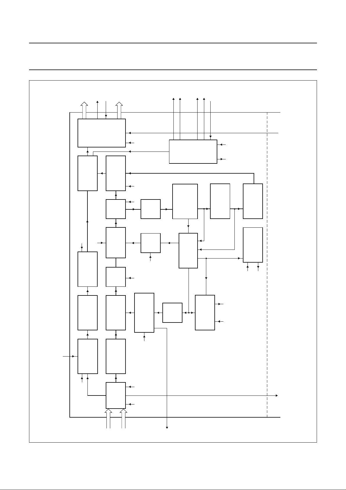
Fig.4 Detailed block diagram; continued in Fig.5.
to luminance from luminance
(7-0)
CUV
CVBS
(7-0)
RTCO
April 1993 10

Philips Semiconductors Product specification
Digital multistandard colour decoder with
SCART interface (DMSD2-SCART)
(3-1)
YDEL
COMPENSATION
VARIABLE DELAY
AND
WEIGHTING
ADDING STAGE
(1-0)
APER
CREF
LL27
4
27
CLOCK
GENERATOR
LINE-LOCKED
DELAY
PROGRAMMABLE
XTAL
XTALI
33
34
CLOCK
CRYSTAL
GENERATOR
(DTO2)
OSCILLATOR
DISCRETE TIME
SAA7151B
MEH295
DAC
ndbook, full pagewidth
from input interface to output interface
CORING
FILTER
VARIABLE
BANDPASS
TRAP
CHROMINANCE
PRE-FILTER
CONVERTER
SAMPLE RATE
CORI
PREF
BYPS
(1-0)
BYPS BPSS
PREF
OFFSET
MATCHING
AMPLIFIER
LUMINANCE
COMPENSATION
LOOP
FILTER
COARSE
PHASE DETECTOR
FINE
PHASE DETECTOR
SYNC SLICER
SYNC
PRE-FILTER
HPLL
HLCK
HLCK
VTRC
HCLB (7-0)
HCLS (7-0)
HSYB (7-0)
HSYS (7-0)
SCEN
SAA7151B
VNOI (1-0)
WIND
BOFL
BFON
SYNC
HPHI (7-0)
IDEL (7-0)
OEVS
OEHS
FSEL
41
HLCK
C-BUS
2
I
AUFD
VERTICAL
PROCESSOR
COUNTER
CONTROL
40
FIDT
39 36
ODD
29 30 31
HSY VS HS LFCO
26
HCLGPSW0
Fig.5 Detailed block diagram; continued from Fig.4.
63
43
April 1993 11
SCL
SDA
IICSA

Philips Semiconductors Product specification
Digital multistandard colour decoder with
SAA7151B
SCART interface (DMSD2-SCART)
Table 2 for the 4:2:2 format (720 pixels per line). The quoted frequencies are valid on the YUV-bus. The time
frames are controlled by the HREF signal.
OUTPUT PIXEL BYTE SEQUENCE
Y0 (LSB) Y0 Y0 Y0 Y0 Y0 Y0
Y1 Y1 Y1 Y1 Y1 Y1 Y1
Y2 Y2 Y2 Y2 Y2 Y2 Y2
Y3 Y3 Y3 Y3 Y3 Y3 Y3
Y4 Y4 Y4 Y4 Y4 Y4 Y4
Y5 Y5 Y5 Y5 Y5 Y5 Y5
Y6 Y6 Y6 Y6 Y6 Y6 Y6
Y7 (MSB) Y7 Y7 Y7 Y7 Y7 Y7
UV0 (LSB) U0 V0 U0 V0 U0 V0
UV1 U1 V1 U1 V1 U1 V1
UV2 U2 V2 U2 V2 U2 V2
UV3 U3 V3 U3 V3 U3 V3
UV4 U4 V4 U4 V4 U4 V4
UV5 U5 V5 U5 V5 U5 V5
UV6 U6 V6 U6 V6 U6 V6
UV7 (MSB) U7 V7 U7 V7 U7 V7
Y frame 012345
UV frame 0 2 4
Table 3 for the 4:1:1 format (720 pixels per line). The quoted frequencies are valid on the YUV-bus. The time
frames are controlled by the HREF signal.
OUTPUT PIXEL BYTE SEQUENCE
Y0 (LSB) Y0 Y0 Y0 Y0 Y0 Y0 Y0 Y0
Y1 Y1 Y1 Y1 Y1 Y1 Y1 Y1 Y1
Y2 Y2 Y2 Y2 Y2 Y2 Y2 Y2 Y2
Y3 Y3 Y3 Y3 Y3 Y3 Y3 Y3 Y3
Y4 Y4 Y4 Y4 Y4 Y4 Y4 Y4 Y4
Y5 Y5 Y5 Y5 Y5 Y5 Y5 Y5 Y5
Y6 Y6 Y6 Y6 Y6 Y6 Y6 Y6 Y6
Y7 (MSB) Y7 Y7 Y7 Y7 Y7 Y7 Y7 Y7
UV0 (LSB) 0 0 0 0 0 0 0 0
UV1 0 0 0 0 0 0 0 0
UV2 0 0 0 0 0 0 0 0
UV3 0 0 0 0 0 0 0 0
UV4 V6 V4 V2 V0 V6 V4 V2 V0
UV5 V7 V5 V3 V1 V7 V5 V3 V1
UV6 U6 U4 U2 U0 U6 U4 U2 U0
UV7 (MSB) U7 U5 U3 U1 U7 U5 U3 U1
Y frame 0 1 2 3 4 5 6 7
UV frame 0 4
April 1993 12
Philips Semiconductors Product specification
Digital multistandard colour decoder with
SAA7151B
SCART interface (DMSD2-SCART)
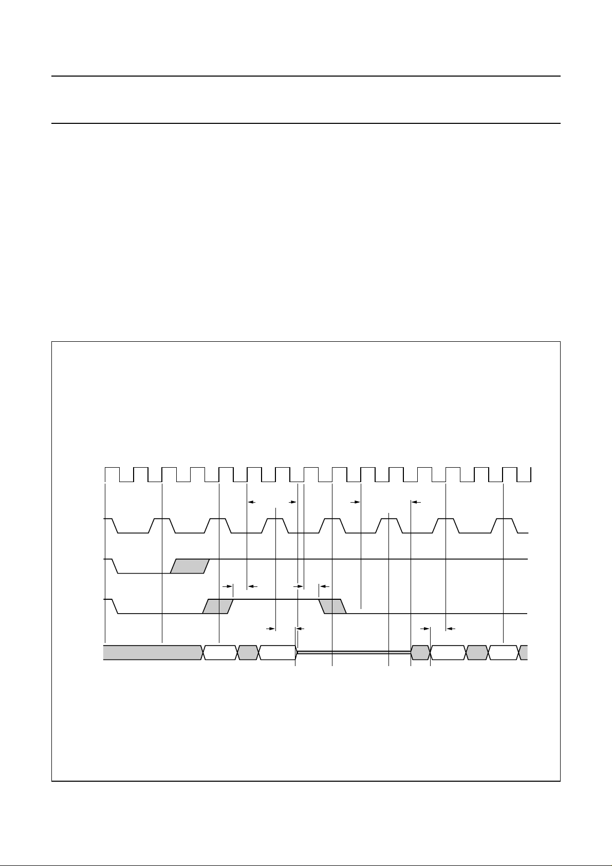
Signal levels (Figures 12, 13 and 14) The nominal input and output signal levels are defined by a colour bar signal with 75 % colour, 100 % saturation and
100 % luminance amplitude (EBU colour bar).
CUV-bus input format
The CUV-bus transfers the digital chrominance/colour-difference signals from the ADC to the SAA7151B (Fig.6; Table 1):
• normal mode for digital chrominance transmission.
• UV colour-difference mode for colour-difference signals UV (out of matrixed RGB signals)
• FS mode (fast switch mode; UV inserted into chrominance signal C with addition of the two signal spectra).
RTCO output
The RTCO output signal (Fig.10) contains serialized information about actual clock frequency, subcarrier frequency and
PAL/SECAM sequence. This signal may preferably be used with the frequency-locked digital video encoder SAA7199B.
handbook, full pagewidth
LL27
CREF
HREF
FEIN
YUV
to 3-state
t
OH
t
HD
t
SU
from 3-state
Fig.6 Timing example of fast enable input (FEIN).
t
OS
MEH548
April 1993 13

Philips Semiconductors Product specification
Digital multistandard colour decoder with
SCART interface (DMSD2-SCART)
handbook, full pagewidth
LL27 clock
LL13.5 clock
MUXC
012
0
SAA7151B
345
12
Normal mode (chrominance pixel byte sequence)
chrominance
UV colour-difference mode (UV pixel byte sequence)
colour-
difference
valid colourdifference
Fast switch mode (data insertion)
CUV
valid CUV
C0
V0
U0 V1 U3
(V0 + C0)/2
C1
V1
(V1 + C1)/2
C2
U2
(1) (1) (1)
(U2 + C2)/2
(1) (1) (1)
(V1 + C1)/2 (U3 + C3)/2
C3
U3
(U3 + C3)/2
C4
V4
(V4 + C0)/2
C5
V5
V5
(V5 + C5)/2
(V5 + C5)/2
MEH332
Fig.7 CUV input formats.
(1) each second sample only after a MUXC change is taken for down-sampling to 13.5 MHz to reduce
cross-talk components between U and V signals.
April 1993 14
Philips Semiconductors Product specification
Digital multistandard colour decoder with
SCART interface (DMSD2-SCART)
handbook, full pagewidth
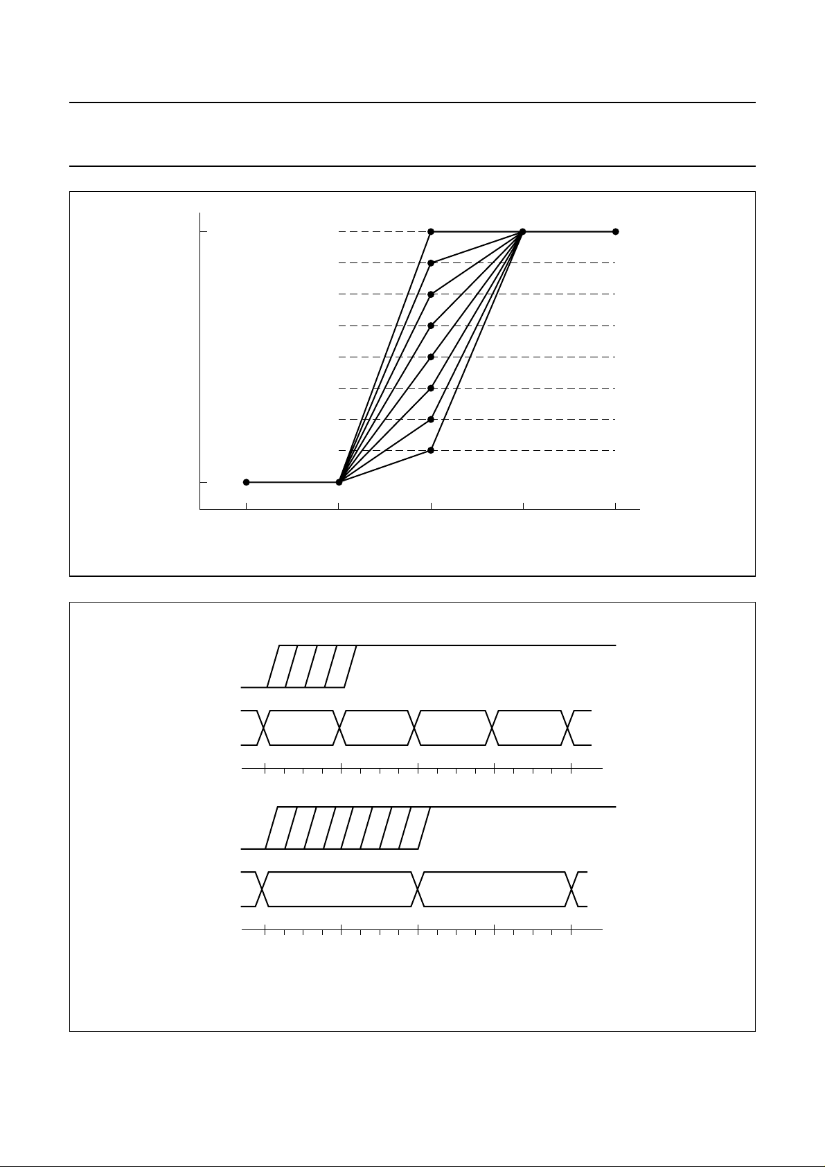
new
old
0 old + 1 new
1/8 old + 7/8 new
1/4 old + 3/4 new
3/8 old + 5/8 new
1/2 old + 1/2 new
5/8 old + 3/8 new
3/4 old + 1/4 new
7/8 old + 1/8 new
T(n−2) T(n−1) T(n)
Note: in 4:2:2 format weighting
in 1/4 steps only.
T(n+1) T(n+2)
SAA7151B
MEH307
handbook, full pagewidth
FS
UV
LL6.75
LL27
FS
UV
LL3.375
LL27
Fig.8 Addition of weighted components.
1
3/4 1/2 1/4 fast switch weighting for 4:2:2 format
U0, V0 U1, V1
01
012
013
01234
34
5678910111213141516
1 7/8 3/4 5/8 1/2 3/8 1/4 1/8
U0, V0
5678910111213141516
U2, V2 U3, V3
234
fast switch weighting for 4:1:1 format
U1, V1
MEH308
Fig.9 Weighting factors of fast switching for 4:2:2 and 4:1:1 formats.
April 1993 15
 Loading...